OPTICAL SEMICONDUCTOR DEVICE MODULE
US20110249449A1
2011-10-13
12/958,438
2010-12-02
Abstract:
An optical semiconductor device module comprises: a stem; an optical semiconductor device mounted on the stem; a cap fixed on the stem and covering the optical semiconductor device; a plastic lens fixed to the cap and collecting outgoing light from the optical semiconductor device; and a glass plate fixed to the cap and sealing the optical semiconductor device.
Assignee:
- MITSUBISHI ELECTRIC CORPORATION 16,245 🇯🇵 TOKYO, Japan
Interested in similar patents?
Get notified when new applications in this technology area are published.
Classification:
G02B6/4204 » CPC main
Light guides; Coupling light guides; Coupling light guides with opto-electronic elements; Packages, e.g. shape, construction, internal or external details the coupling comprising intermediate optical elements, e.g. lenses, holograms
G02B6/4202 » CPC further
Light guides; Coupling light guides; Coupling light guides with opto-electronic elements; Packages, e.g. shape, construction, internal or external details for coupling an active element with fibres without intermediate optical elements, e.g. fibres with plane ends, fibres with shaped ends, bundles
F21V3/04 IPC
Globes; Bowls; Cover glasses characterised by materials, surface treatments or coatings
Description
BACKGROUND OF THE INVENTION
1. Field of the Invention
The present invention relates to an optical semiconductor device module for optical communications, and in particular to an optical semiconductor device module capable of sufficiently sealing an optical semiconductor device and reducing the manufacturing costs.
2. Background Art
In an optical semiconductor device module for optical communications, a lens for collecting outgoing light of the optical semiconductor device is fixed to a cap. Conventionally, a glass lens has been used as a lens. By the glass lens, both the seal of the optical semiconductor device and light collecting have been realized (for example, refer to Japanese Patent Application Laid-Open No. 2005-352075).
SUMMARY OF THE INVENTION
However, since the glass lens is expensive, the manufacturing costs of conventional optical semiconductor device module are high. On the other hand, although plastic lenses are available as inexpensive lenses, the plastic lenses cannot sufficiently seal the optical semiconductor device due to the relationship with other materials. Therefore, inexpensive plastic lenses have not been used for optical semiconductor device modules for optical communications that require sealing.
In view of the above-described problems, an object of the present invention is to provide an optical semiconductor device module capable of sufficiently sealing an optical semiconductor device and reducing the manufacturing costs.
According to the present invention, an optical semiconductor device module comprises: a stem; an optical semiconductor device mounted on the stem; a cap fixed on the stem so as to cover the optical semiconductor device; a plastic lens fixed to the cap and collecting an outgoing light from the optical semiconductor device; and a glass plate fixed to the cap and sealing the optical semiconductor device.
The present invention makes it possible to sufficiently seal an optical semiconductor device and reduce the manufacturing costs.
Other and further objects, features and advantages of the invention will appear more fully from the following description.
BRIEF DESCRIPTION OF THE DRAWINGS
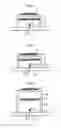
FIG. 1 is a sectional view showing an optical semiconductor device module according to the first embodiment.
FIG. 2 is a sectional view showing a modification example of an optical semiconductor device module according to the first embodiment.
FIG. 3 is a sectional view showing an optical semiconductor device module according to the second embodiment.
FIG. 4 is a sectional view showing a first modification example of an optical semiconductor device module according to the second embodiment.
FIG. 5 is a sectional view showing a second modification example of an optical semiconductor device module according to the second embodiment.
FIG. 6 is a sectional view showing an optical semiconductor device module according to the third embodiment.
FIG. 7 is a sectional view showing a modification example of the optical semiconductor device module according to the third embodiment.
FIG. 8 is a sectional view showing an optical semiconductor device module according to the fourth embodiment.
DETAILED DESCRIPTION OF THE PREFERRED EMBODIMENTS
Now, embodiments of the present invention will be described with reference to the drawings. Same reference numerals denote same components throughout the drawings, and redundant descriptions will be omitted.
First Embodiment
FIG. 1 is a sectional view showing an optical semiconductor device module according to the first embodiment. A semiconductor laser 4 (optical semiconductor device) is mounted on the stem 1 via a heat sink 2 and the sub-mount 3. A cap 5 is fixed on the stem 1 so as to cover the semiconductor laser 4. A plastic lens 6 and a glass plate 7 are fixed to the cap 5. The plastic lens 6 collects the outgoing light from the semiconductor laser 4. The glass plate 7 seals the semiconductor laser 4.
By thus using the glass plate 7, the semiconductor laser 4 can be sufficiently sealed. By using the plastic lens 6, the manufacturing costs can be reduced.
FIG. 2 is a sectional view showing a modification example of an optical semiconductor device module according to the first embodiment. The cap 5 has a mark 8 (guide) on the location where the plastic lens 6 is installed. By the mark 8, the plastic lens 6 can be accurately fixed to the location in the cap 5.
Second Embodiment
FIG. 3 is a sectional view showing an optical semiconductor device module according to the second embodiment. A cap 5a (first cap) wherein the plastic lens 6 is installed and a cap 5b (second cap) wherein the glass plate 7 is installed are different members. The cap 5a is overlapped on the cap 5b. Thereby, caps 5a and 5b can be fabricated by using conventional techniques.
FIG. 4 is a sectional view showing a first modification example of an optical semiconductor device module according to the second embodiment. In this modification example, the cap 5s is overlapped on the cap 5b, and the plastic lens 6 is nearer to the semiconductor laser 4 than the glass plate 7. Thereby, since the plastic lens 6 becomes close to the light-emitting region, light collecting becomes easier.
FIG. 5 is a sectional view showing a second modification example of an optical semiconductor device module according to the second embodiment. In this modification example, the upper cap 5a is fitted in the lower cap 5b. Thereby, since the location of the upper cap 5a is automatically determined when the location of the lower cap 5b is determined, no alignment is required.
Third Embodiment
FIG. 6 is a sectional view showing an optical semiconductor device module according to the third embodiment. A cap 5a wherein the plastic lens 6 is installed and a cap 5b wherein the glass plate 7 is installed are different members. The cap 5a and the cap 5b are fixed to the stem 1, respectively. The cap 5a covers the cap 5b. Thereby, the caps 5a and 5b can be fabricated by using conventional techniques, and the caps 5a and 5b can be fixed to the stem 1 by using conventional techniques.
FIG. 7 is a sectional view showing a modification example of the optical semiconductor device module according to the third embodiment. In this modification example, the internal wall of the external cap 5a contacts the external wall of the internal cap 5b. Thereby, since the location of the external cap 5a is automatically determined when the location of the internal cap 5b is determined, no alignment is required.
Fourth Embodiment
FIG. 8 is a sectional view showing an optical semiconductor device module according to the fourth embodiment. In the present embodiment, a coating film 9 such as silicon nitride or silicon oxide is placed in place of the glass plate 7 described in the first to third embodiments. The coating film 9 coats the cap 5 over the plastic lens 6 and seals the semiconductor laser 4. Thereby, effects equivalent to the effects of the first embodiment can be obtained. The coating film 9 may be placed inside the cap 5.
Obviously many modifications and variations of the present invention are possible in the light of the above teachings. It is therefore to be understood that within the scope of the appended claims the invention may be practiced otherwise than as specifically described.
The entire disclosure of a Japanese Patent Application No. 2010-090089, filed on Apr. 9, 2010 including specification, claims, drawings and summary, on which the Convention priority of the present application is based, are incorporated herein by reference in its entirety.
Claims
1. An optical semiconductor device module comprising:
a stem;
an optical semiconductor device mounted on the stem;
a cap fixed on the stem and covering the optical semiconductor device;
a plastic lens fixed to the cap and collecting outgoing light from the optical semiconductor device; and
a glass plate fixed to the cap and sealing the optical semiconductor device.
2. The optical semiconductor device module according to claim 1, wherein the cap has a mark on a location where the plastic lens is installed.
3. The optical semiconductor device module according to claim 1, wherein
the cap includes a first cap on which the plastic lens is installed and a second cap on which the glass plate is installed, and
one of the first cap and the second cap overlaps the other.
4. The optical semiconductor device module according to claim 3, wherein the second cap overlaps the first cap, and the plastic lens is nearer to the optical semiconductor device than is the glass plate.
5. The optical semiconductor device module according to claim 3, wherein the upper one of the first cap and the second cap is fitted in the lower one of the first cap and the second cap.
6. The optical semiconductor device module according to claim 1, wherein
the cap includes a first cap on which the plastic lens is installed, and a second cap on which the glass plate is installed,
the first cap and the second cap are fixed on the stem, and
one of the first cap and the second cap covers the other.
7. The optical semiconductor device module according to claim 6, wherein an internal wall of the external one of the first cap and the second cap contacts an external wall of the internal one of the first cap and the second cap.
8. The optical semiconductor device module comprising:
an optical semiconductor device;
a stem on which the optical semiconductor device is mounted;
a cap fixed on the stem and covering the optical semiconductor device;
a plastic lens fixed to the cap and collecting outgoing light from the optical semiconductor device; and
a coating film coating the cap and sealing the optical semiconductor device.
Images & Drawings included:


Sources:
- United States Patent and Trademark Office - verify current appl. status at the USPTO↗
Similar patent applications:
- » 20120033284
Semiconductor optical modulation device, Mach-Zehnder interferometer type semiconductor optical modulator, and method for producing semiconductor optical modulation device - » 20210175682
Electro-absorption modulator, optical semiconductor device and optical module - » 20130209021
Optical semiconductor modulator device and optical module - » 20180048116
Semiconductor optical device, optical module, and method for manufacturing semiconductor optical device - » 20200287090
Semiconductor optical device, optical module, and manufacturing method of semiconductor optical device - » 20180090910
Optical semiconductor device, optical module, and method for manufacturing optical semiconductor device - » 20080144151
Optical device, semiconductor laser module, optical scanning device, and image forming apparatus - » 20100091630
METHOD FOR MANUFACTURING SEMICONDUCTOR DEVICE, OPTICAL PICKUP MODULE AND SEMICONDUCTOR DEVICE - » 20050139843
Structure of chip carrier for semiconductor optical device, optical module, and optical transmitter and receiver - » 20090097804
Optical subassembly of optical semiconductor device module and assembly method thereof
Recent applications in this class:
- » 20250067943 2025-02-27
IMAGE SENSING MODULE - » 20240377593 2024-11-14
OPTICAL INTEGRATED DEVICE AND PREPARATION METHOD THEREFOR - » 20240345335 2024-10-17
MICRO LED DISPLAY DEVICE - » 20240319451 2024-09-26
OPTICAL MODULE, OPTICAL CONNECTOR CABLE, AND METHOD FOR PRODUCING OPTICAL MODULE - » 20240302605 2024-09-12
SYSTEMS USING MICROLED-BASED INTERCONNECTS - » 20240272380 2024-08-15
Fast-axis collimator with hanging connector - » 20240201455 2024-06-20
LENS UNIT, OPTICAL WAVEGUIDE DEVICE, AND OPTICAL TRANSMISSION DEVICE - » 20240019645 2024-01-18
Display panel and electronic device - » 20230258881 2023-08-17
PACKAGE STRUCTURE, SEMICONDUCTOR DEVICE AND METHOD OF FABRICATING THE SAME - » 20230221503 2023-07-13
Diffractive optical waveguide and display device
Recent applications for this Assignee:
- » 20250176211 2025-05-29
SEMICONDUCTOR DEVICE AND METHOD OF MANUFACTURING SEMICONDUCTOR DEVICE - » 20250176196 2025-05-29
SEMICONDUCTOR DEVICE - » 20250175212 2025-05-29
COMMUNICATION DEVICE - » 20250175160 2025-05-29
NOISE FILTER - » 20250175128 2025-05-29
POWER AMPLIFIER - » 20250175049 2025-05-29
ARMATURE AND ELECTRIC MOTOR - » 20250173505 2025-05-29
INFORMATION PROCESSING SYSTEM, INFORMATION PROCESSING DEVICE, INFORMATION PROCESSING METHOD, AND RECORDING MEDIUM - » 20250173242 2025-05-29
LOG DATA ANALYSIS ASSISTANCE SYSTEM, LOG DATA ANALYSIS ASSISTANCE METHOD, RECORDING MEDIUM, AND ASSISTANCE DEVICE - » 20250173200 2025-05-29
CONTROL DEVICE, CONTROL METHOD, AND PROGRAM - » 20250173128 2025-05-29
RECORDING MEDIUM, PROGRAMMING ASSISTING DEVICE, AND PROGRAMMING ASSISTING METHOD