Electronic device housing and method for making the same
US20110256361A1
2011-10-20
12/949,955
2010-11-19
✅ Patent granted
US 8,507,107 B2
2013-08-13
-
-
Mark Ruthkosky | Laura C Dettinger
Altis Law Group, Inc.
2031-05-06
Abstract:
An electronic device housing is provided. The electronic device housing includes a substrate, a first metallic coating formed on the substrate, and a second metallic coating formed on a portion of the first metallic coating. The first and second metallic coatings are formed by vacuum sputtering or vacuum vapor deposition. The first and second metallic coatings are all non-conductive. A method for making the electronic device housing is also described there.
Inventors:
- CHWAN-HWA CHIANG 35 🇹🇼 Shindian, Taiwan
- QI-JIAN DU 14 🇨🇳 ShenZhen City, China
- QI-JIAN DU 9 🇨🇳 Shenzhen, China
- Chwan-Hwa Chiang 10 🇹🇼 Taipei Hsien, Taiwan
Assignee:
- FIH (HONG KONG) LIMITED 1,465 🇭🇰 Kowloon, Hong Kong
- SHENZHEN FUTAIHONG PRECISION INDUSTRY CO., LTD. 1,108 🇨🇳 ShenZhen City, China
- SHENZHEN FUTAIHONG PRECISION INDUSTRY CO., LTD. 413 🇨🇳 Shenzhen, China
Applicant:
Interested in similar patents?
Get notified when new applications in this technology area are published.
Classification:
B32B9/00 IPC
Layered products characterised by particular substances used
B32B9/00 IPC
Layered products comprising a layer of a particular substance not covered by groups -
H05K5/0243 » CPC main
Casings, cabinets or drawers for electric apparatus; Details; Mechanical details of casings for decorative purposes
H05K5/0243 » CPC main
Casings, cabinets or drawers for electric apparatus; Details; Mechanical details of casings for decorative purposes
Y10T428/12 » CPC further
Stock material or miscellaneous articles All metal or with adjacent metals
Y10T428/131 » CPC further
Stock material or miscellaneous articles; Hollow or container type article [e.g., tube, vase, etc.] Glass, ceramic, or sintered, fused, fired, or calcined metal oxide or metal carbide containing [e.g., porcelain, brick, cement, etc.]
Y10T428/24628 » CPC further
Stock material or miscellaneous articles; Structurally defined web or sheet [e.g., overall dimension, etc.] Nonplanar uniform thickness material
Y10T428/24802 » CPC further
Stock material or miscellaneous articles; Structurally defined web or sheet [e.g., overall dimension, etc.] Discontinuous or differential coating, impregnation or bond [e.g., artwork, printing, retouched photograph, etc.]
Y10T428/264 » CPC further
Stock material or miscellaneous articles; Web or sheet containing structurally defined element or component, the element or component having a specified physical dimension; Coating layer not in excess of 5 mils thick or equivalent Up to 3 mils
Y10T428/265 » CPC further
Stock material or miscellaneous articles; Web or sheet containing structurally defined element or component, the element or component having a specified physical dimension; Coating layer not in excess of 5 mils thick or equivalent; Up to 3 mils 1 mil or less
B32B3/10 IPC
Layered products comprising a layer with external or internal discontinuities or unevennesses, or a layer of non-planar form ; Layered products having particular features of form characterised by a discontinuous layer, i.e. formed of separate pieces of material
B32B15/04 IPC
Layered products comprising a layer of metal comprising metal as the main or only constituent of a layer, next to another layer of a
C23C14/34 IPC
Coating by vacuum evaporation, by sputtering or by ion implantation of the coating forming material characterised by the process of coating Sputtering
B32B17/06 IPC
Layered products essentially comprising sheet glass, or glass, slag, or like fibres comprising glass as the main or only constituent of a layer, next to another layer of a specific material
B32B1/00 IPC
Layered products having a general shape other than plane
B32B3/00 IPC
Layered products comprising a layer with external or internal discontinuities or unevennesses, or a layer of non-planar form ; Layered products having particular features of form
B22D11/00 IPC
Particular casting processes; Machines or apparatus therefor
B22D11/00 IPC
Continuous casting of metals, i.e. casting in indefinite lengths
H02B1/00 IPC
Frameworks, boards, panels, desks, casings; Details of substations or switching arrangements
B32B15/00 IPC
Layered products comprising a layer of metal
Description
CROSS-REFERENCE TO RELATED APPLICATIONS
This application is one of the three related co-pending U.S. patent applications listed below. All listed applications have the same assignee. The disclosure of each of the listed applications is incorporated by reference into all the other listed applications.
| Attorney | Application | Filing | ||
| Docket No. | Title | Inventors | No. | Date |
| US 31154 | ELECTRONIC | QI-JIAN | 12/891,904 | 2010/9/28 |
| DEVICE | DU et al. | |||
| HOUSING | ||||
| US 31522 | ELECTRONIC | QI-JIAN | — | — |
| DEVICE | DU et al. | |||
| HOUSING | ||||
| US 33355 | ELECTRONIC | QI-JIAN | — | — |
| DEVICE | DU et al. | |||
| HOUSING AND | ||||
| METHOD FOR | ||||
| MAKING THE | ||||
| SAME | ||||
BACKGROUND
1. Technical Field
The present disclosure relates to electronic device housings, particularly to an electronic device housing having a metallic and changeable color appearance pattern, and a method for making the electronic device housing.
2. Description of Related Art
Decorative metallic coatings are often deposited on housings of electronic devices. The metallic coatings are typically formed by vacuum deposition and are nonconductive so they do not block electromagnetic waves. These metallic coatings may be transparent or translucent. However, the metallic coatings cannot present a changeable color appearance pattern.
Therefore, there is room for improvement within the art.
BRIEF DESCRIPTION OF THE FIGURES
Many aspects of the electronic device housing can be better understood with reference to the following figures. The components in the figures are not necessarily drawn to scale, the emphasis instead being placed upon clearly illustrating the principles of the electronic device housing. Moreover, in the drawings like reference numerals designate corresponding parts throughout the several views.
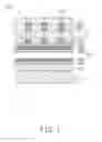
FIG. 1 is a cross-section of an electronic device housing according to an exemplary embodiment;
FIG. 2 is another cross-section of an exemplary embodiment of the electronic device housing.
DETAILED DESCRIPTION
FIG. 1 and FIG. 2 show an electronic device housing 10 according to different exemplary embodiments. The electronic device housing 10 includes a substrate 11, a base paint coating 13 formed on a surface of the substrate 11, a first metallic coating 15 formed on the base paint coating 13, a second metallic coating 17 formed on a portion of the first metallic coating 15, and a top paint coating 19 formed on the second metallic coating 17 and the first metallic coating 15. The electronic device housing 10 may be a housing of a mobile phone, personal digital apparatus (PDA), note book computer, MP3, MP4, GPS navigator, or digital camera.
The substrate 11 may be made of plastic selected from a group consisting of polycarbonate (PC), polyethylene (PE), polymethyl methacrylate (PMMA), and a mixture of polycarbonate and acrylonitrile-butadiene-styrene plastics (PC+ABS). The substrate 11 may instead be made of glass, ceramic, or metal.
The base paint coating 13 may be an acrylic resin paint coating. The base paint coating 13 may have a thickness of about 1 μm to about 30 μm. The base paint coating 13 has a smooth surface for enhancing the bond between the base paint coating 13 and subsequent coatings. The base paint coating 13 may be colored to present a colorful appearance for the electronic device housing 10.
The first metallic coating 15 may be formed on the base paint coating 13 by vacuum sputtering or vacuum vapor deposition. The metallic coating 15 may include a number of first layers 151 interleaved with a number of second layers 153, with a second layer 153 or a first layer 151 outermost on the interleaving pattern. The number of first layers 151 and the number of second layers 153 may include three to seven layers in total. The first layer 151 and the second layer 153 may be respectively niobium pentoxide (Nb2O5) layer and silicon dioxide (SiO2) layer. Either one niobium pentoxide layer (FIG. 2) or either one silicon dioxide layer (FIG. 1) may be directly formed on the base paint coating 13. The total thickness of the first metallic coating 15 may be of about 50-500 nm. The thickness of the first metallic coating 15 is determined by the thickness needed for presenting a metallic appearance for the electronic device housing 10 without interfering with radio transmission capabilities.
The second metallic coating 17 may be formed on a portion of the surface of the first metallic coating 15 by vacuum sputtering or vacuum vapor deposition. The second metallic coating 17 may include a number of first layers 171 interleaved with a number of second layers 173, with a second layer 173 or a first layer 171 outermost on the interleaving pattern. The number of first layers 171 and the number of second layers 173 may include three to seven layers in total. The first layer 171 and the second layer 173 may be respectively niobium pentoxide (Nb2O5) layer and silicon dioxide (SiO2) layer. Either one of the niobium pentoxide layer may be directly formed on one of the silicon dioxide layers of the first metallic coating 15 (FIG. 1), or either one of the silicon dioxide layers may be directly formed on one of the niobium pentoxide layers of the first metallic coating 15 (FIG. 2). The total thickness of the second metallic coating 17 may be of about 50-500 nm. The thickness of the second metallic coating 17 is determined by the thickness needed for presenting a metallic appearance without interfering with radio transmission capabilities. The second metallic coating 17 defines decorative patterns or letters.
In the region for forming the second metallic coating 17, the first metallic coating 15 and the second metallic coating 17 reflect light under irradiation of visible light at different incident angles. The light reflected by the first metallic coating 15 has different wavelength than the light reflected by the second metallic coating 17, and these different wavelengths form several intensifying interference regions. The different intensifying interference regions, when viewed during relative movement of the electronic device housing 10, will make the electronic device housing 10 appear to be changing and shifting color patterns or letters in the region of the second metallic coating 17, which will be visually interesting and appealing.
The top paint coating 19 may be a transparent paint coating formed on the second metallic coating 17 and the first metallic coating 15. The paint used for the top paint coating 19 may be an ultraviolet (UV) curable paint. The thickness of the top paint coating 19 may be about 10-50 μm. The top paint coating 19 has a high hardness, which protects the first metallic coating 15 and the second metallic coating 17 from abrasion.
It is to be understood that the base paint coating 13 may be omitted, and the first metallic coating 15 is directly formed on the substrate 11.
It is to be understood that the top paint coating 19 may be omitted in applications where abrasion of the electronic device housing 10 is not a concern.
A method for making the electronic device housing 10 may include the following steps.
The substrate 11 is provided. The substrate 11 may be made of plastic, glass, ceramic, or metal.
The base paint coating 13 is sprayed on the substrate 11.
The first metallic coating 15 is formed on the base paint coating 13 by vacuum sputtering or vacuum vapor deposition.
A mask having a cut out pattern is provided (not shown in the figures). The mask then covers on the first metallic coating 15. The mask may be a soft plastic film, such as polythene film. The mask has a thickness of about less than 1 mm. The pattern of the mask forms decorative patterns or letters.
A vacuum sputtering process or a vacuum vapor depositing process is implemented on the mask and the cut out pattern of the mask forms a metallic coating. The metallic coating formed by the pattern directly bonds with the first metallic coating 15. After that, the mask is removed and accordingly, the metallic coating formed on the mask is also removed and remaining is a pattern that has been formed on the metallic coating ready to receive the second metallic coating 17.
The top paint coating 19 is sprayed on the first metallic coating 15 and the second metallic coating 17.
It should be understood, however, that though numerous characteristics and advantages of the present embodiments have been set forth in the foregoing description, together with details of functions of the embodiments, the disclosure is illustrative only, and changes may be made in detail within the principles of the disclosure to the full extent indicated by the broad general meaning of the terms in which the appended claims are expressed.
Claims
What is claimed is:1. An electronic device housing, comprising:
a substrate;
a first metallic coating formed on the substrate by vacuum sputtering or vacuum vapor deposition; and
a second metallic coating formed on a portion surface of the first metallic coating by vacuum sputtering or vacuum vapor deposition.
2. The electronic device housing as claimed in claim 1, wherein the second metallic coating defines decorative patterns or letters.
3. The electronic device housing as claimed in claim 1, wherein the first metallic coating includes a number of first layers interleaved with a number of second layers, with a first layer or a second layer outermost on the interleaving pattern; the first layer and the second layer are respectively niobium pentoxide layer and silicon dioxide layer.
4. The electronic device housing as claimed in claim 1, wherein the first metallic coating has a thickness of about 50-500 nm.
5. The electronic device housing as claimed in claim 4, wherein the first metallic coating presents a metallic appearance without interfering with radio transmission capabilities.
6. The electronic device housing as claimed in claim 3, wherein the number of first layers and the number of second layers include three to seven layers in total.
7. The electronic device housing as claimed in claim 3, wherein the second metallic coating includes a number of first layers interleaved with a number of second layers, with a second layer or a first layer outermost on the interleaving pattern; the first layer and the second layer are respectively niobium pentoxide layer and silicon dioxide layer.
8. The electronic device housing as claimed in claim 1, wherein the second metallic coating has a thickness of about 50-500 nm.
9. The electronic device housing as claimed in claim 8, wherein the second metallic coating presents a metallic appearance without interfering with radio transmission capabilities.
10. The electronic device housing as claimed in claim 7, wherein the number of first layers and the number of second layers include three to seven layers in total.
11. The electronic device housing as claimed in claim 7, wherein one of the niobium pentoxide layers of the second metallic coating is directly formed on one of the silicon dioxide layers of the first metallic coating.
12. The electronic device housing as claimed in claim 7, wherein one of the silicon dioxide layers of the second metallic coating is directly formed on one of the niobium pentoxide layers of the first metallic coating.
13. The electronic device housing as claimed in claim 1, further comprising a base paint coating formed between the substrate and the first metallic coating.
14. The electronic device housing as claimed in claim 13, wherein the base paint coating is an acrylic resin paint coating and has a thickness of about 1-30 μm.
15. The electronic device housing as claimed in claim 1, further comprising a top paint coating formed on the first metallic coating and the second metallic coating.
16. The electronic device housing as claimed in claim 15, wherein the top paint coating is an ultraviolet curable paint coating having a thickness of about 10-50 μm.
17. The electronic device housing as claimed in claim 1, wherein the substrate is made of plastic, glass, ceramic or metal.
18. A method for making electronic device housing, comprising:
providing a substrate;
vacuum sputtering or vacuum vapor depositing a first metallic coating on the substrate;
providing a mask having a cut out pattern;
covering the mask on the first metallic coating;
vacuum sputtering or vacuum vapor depositing a metallic coating on the mask and the cut out pattern; and
removing the mask to form a second metallic coating on the first metallic coating.
19. The method as claimed in claim 18, further comprising a step of spraying a base paint coating on the substrate before forming the first metallic coating.
20. The method as claimed in claim 18, further comprising a step of spraying a top paint coating on the second metallic coating and the first metallic coating.
Images & Drawings included:


Sources:
- United States Patent and Trademark Office - verify current appl. status at the USPTO↗
Similar patent applications:
- » 20130257237
Housing for electronic devices and method for making housing - » 20200094518
THIN, HIGH-STIFFNESS LAMINATES, PORTABLE ELECTRONIC DEVICE HOUSINGS INCLUDING THE SAME, AND METHODS FOR MAKING SUCH LAMINATES AND PORTABLE ELECTRONIC DEVICE HOUSINGS - » 20140368388
HOUSING OF ELECTRONIC DEVICE, AND METHOD FOR MAKING THE HOUSING - » 20090305001
HOUSING FOR ELECTRONIC DEVICE AND METHOD FOR MAKING THE HOUSING - » 20100108344
Housing for electronic device and method of making the housing - » 20090009935
HOUSING FOR AN ELECTRONIC DEVICE AND METHOD FOR MAKING THE HOUSING - » 20130240350
ELECTRONIC DEVICE HOUSING AND METHOD FOR MAKING THE SAME - » 20110159258
Electronic device housing and method for making the same - » 20060092601
Method of making an electronic device housing - » 20120189842
ELECTRONIC DEVICE HOUSING AND METHOD FOR MAKING THE SAME
Recent applications in this class:
- » 20250267808 2025-08-21
DECORATIVE PLATE, COVER PLATE AND ELECTRONIC DEVICE - » 20250194033 2025-06-12
ELECTRICAL ENCLOSURE INCLUDING IN-MOLD DECORATION - » 20250185196 2025-06-05
ELECTRONIC DEVICE COMPRISING HOUSING WITH PATTERN, AND METHOD FOR FORMING PATTERN - » 20250176124 2025-05-29
DECORATIVE SUBSTRATE AND PREPARATION METHOD THEREFOR, COVER PLATE AND ELECTRONIC DEVICE - » 20250176123 2025-05-29
Decorative Plate and Preparation Method Therefor, and Electronic Device - » 20250113451 2025-04-03
DEEP-COLORED HOUSING AND ELECTRONIC DEVICE COMPRISING SAME - » 20250056744 2025-02-13
Housing Assembly, Housing Assembly Preparation Method, and Electronic Device - » 20250024617 2025-01-16
Decorative Plate and Manufacturing Method Therefor, and Electronic Device - » 20240298415 2024-09-05
Electrical Control Console for Watercraft - » 20240215185 2024-06-27
FOLDABLE ELECTRONIC DEVICES
Recent applications for this Assignee:
- » 20220140846 2022-05-05
Antenna structure and wireless communication device using same - » 20220094077 2022-03-24
Antenna structure and wireless communication device using same - » 20220059931 2022-02-24
Antenna structure and wireless communication device - » 20220021116 2022-01-20
Single antenna structure capable of operating in multiple band widths - » 20220010948 2022-01-13
Anti-loosing structure and backlight module - » 20210006324 2021-01-07
Method for determining a communication path of millimeter wave signal, measurement device and measurement controller using the same - » 20200170133 2020-05-28
Housing, electronic device, and method for manufacturing same - » 20200170133 2020-05-28
Housing, electronic device, and method for manufacturing same - » 20200122194 2020-04-23
Frame and surface treatment method for the frame - » 20200122194 2020-04-23
Frame and surface treatment method for the frame