Generation of multiple diameter nanowire field effect transistors
US20110278539A1
2011-11-17
12/778,526
2010-05-12
✅ Patent granted
US 8,519,479 B2
2013-08-27
-
-
Yu-Hsi D Sun
Cantor Colburn LLP | Vazken Alexanian
2031-07-08
Abstract:
A method of modifying a wafer having a semiconductor disposed on an insulator is provided and includes forming first and second nanowire channels connected at each end to semiconductor pads at first and second wafer regions, respectively, with second nanowire channel sidewalls being misaligned relative to a crystallographic plane of the semiconductor more than first nanowire channel sidewalls and displacing the semiconductor toward an alignment condition between the sidewalls and the crystallographic plane such that thickness differences between the first and second nanowire channels reflect the greater misalignment of the second nanowire channel sidewalls.
Inventors:
- Sarunya Bangsaruntip 63 🇺🇸 Mount Kisco, NY, United States
- Jeffrey W. Sleight 271 🇺🇸 Ridgefield, CT, United States
- Guy M. Cohen 72 🇺🇸 Mohegan Lake, NY, United States
Assignee:
- INTERNATIONAL BUSINESS MACHINES CORPORATION 136,239 🇺🇸 ARMONK, NY, United States
Applicant:
Interested in similar patents?
Get notified when new applications in this technology area are published.
Classification:
H01L29/0665 » CPC main
Semiconductor devices adapted for rectifying, amplifying, oscillating or switching, or capacitors or resistors with at least one potential-jump barrier or surface barrier, e.g. PN junction depletion layer or carrier concentration layer; Details of semiconductor bodies or of electrodes thereof; Multistep manufacturing processes therefor; Semiconductor bodies ; Multistep manufacturing processes therefor characterised by their shape; characterised by the shapes, relative sizes, or dispositions of the semiconductor regions ; characterised by the concentration or distribution of impurities within semiconductor regions characterised by the shape of the body the shape of the body defining a nanostructure
B82Y10/00 » CPC further
Nanotechnology for information processing, storage or transmission, e.g. quantum computing or single electron logic
B82Y30/00 » CPC further
Nanotechnology for materials or surface science, e.g. nanocomposites
B82Y40/00 » CPC further
Manufacture or treatment of nanostructures
H01L21/302 » CPC further
Processes or apparatus adapted for the manufacture or treatment of semiconductor or solid state devices or of parts thereof; Manufacture or treatment of semiconductor devices or of parts thereof the devices having at least one potential-jump barrier or surface barrier, e.g. PN junction, depletion layer or carrier concentration layer the devices having semiconductor bodies comprising elements of Group IV of the Periodic System or AB compounds with or without impurities, e.g. doping materials; Treatment of semiconductor bodies using processes or apparatus not provided for in groups - to change their surface-physical characteristics or shape, e.g. etching, polishing, cutting
H01L21/3247 » CPC further
Processes or apparatus adapted for the manufacture or treatment of semiconductor or solid state devices or of parts thereof; Manufacture or treatment of semiconductor devices or of parts thereof the devices having at least one potential-jump barrier or surface barrier, e.g. PN junction, depletion layer or carrier concentration layer the devices having semiconductor bodies comprising elements of Group IV of the Periodic System or AB compounds with or without impurities, e.g. doping materials; Treatment of semiconductor bodies using processes or apparatus not provided for in groups - ; Thermal treatment for modifying the properties of semiconductor bodies, e.g. annealing, sintering for altering the shape, e.g. smoothing the surface
H01L29/045 » CPC further
Semiconductor devices adapted for rectifying, amplifying, oscillating or switching, or capacitors or resistors with at least one potential-jump barrier or surface barrier, e.g. PN junction depletion layer or carrier concentration layer; Details of semiconductor bodies or of electrodes thereof; Multistep manufacturing processes therefor; Semiconductor bodies ; Multistep manufacturing processes therefor characterised by their crystalline structure, e.g. polycrystalline, cubic or particular orientation of crystalline planes by their particular orientation of crystalline planes
H01L29/0673 » CPC further
Semiconductor devices adapted for rectifying, amplifying, oscillating or switching, or capacitors or resistors with at least one potential-jump barrier or surface barrier, e.g. PN junction depletion layer or carrier concentration layer; Details of semiconductor bodies or of electrodes thereof; Multistep manufacturing processes therefor; Semiconductor bodies ; Multistep manufacturing processes therefor characterised by their shape; characterised by the shapes, relative sizes, or dispositions of the semiconductor regions ; characterised by the concentration or distribution of impurities within semiconductor regions characterised by the shape of the body the shape of the body defining a nanostructure; Nanowires or nanotubes oriented parallel to a substrate
H01L29/66439 » CPC further
Semiconductor devices adapted for rectifying, amplifying, oscillating or switching, or capacitors or resistors with at least one potential-jump barrier or surface barrier, e.g. PN junction depletion layer or carrier concentration layer; Details of semiconductor bodies or of electrodes thereof; Multistep manufacturing processes therefor; Types of semiconductor device ; Multistep manufacturing processes therefor; Multistep manufacturing processes of devices having semiconductor bodies comprising group 14 or group 13/15 materials the devices being controllable only by the electric current supplied or the electric potential applied, to an electrode which does not carry the current to be rectified, amplified or switched, e.g. three-terminal devices; Unipolar field-effect transistors with a one- or zero-dimensional channel, e.g. quantum wire FET, in-plane gate transistor [IPG], single electron transistor [SET], striped channel transistor, Coulomb blockade transistor
H01L29/775 » CPC further
Semiconductor devices adapted for rectifying, amplifying, oscillating or switching, or capacitors or resistors with at least one potential-jump barrier or surface barrier, e.g. PN junction depletion layer or carrier concentration layer; Details of semiconductor bodies or of electrodes thereof; Multistep manufacturing processes therefor; Types of semiconductor device ; Multistep manufacturing processes therefor controllable by only the electric current supplied, or only the electric potential applied, to an electrode which does not carry the current to be rectified, amplified or switched; Unipolar devices, e.g. field effect transistors; Field effect transistors with one dimensional charge carrier gas channel, e.g. quantum wire FET
H01L29/04 IPC
Semiconductor devices adapted for rectifying, amplifying, oscillating or switching, or capacitors or resistors with at least one potential-jump barrier or surface barrier, e.g. PN junction depletion layer or carrier concentration layer; Details of semiconductor bodies or of electrodes thereof; Multistep manufacturing processes therefor; Semiconductor bodies ; Multistep manufacturing processes therefor characterised by their crystalline structure, e.g. polycrystalline, cubic or particular orientation of crystalline planes
H01L21/762 IPC
Processes or apparatus adapted for the manufacture or treatment of semiconductor or solid state devices or of parts thereof; Manufacture or treatment of devices consisting of a plurality of solid state components formed in or on a common substrate or of parts thereof; Manufacture of integrated circuit devices or of parts thereof; Manufacture of specific parts of devices defined in group; Making of isolation regions between components Dielectric regions, e.g. EPIC dielectric isolation, LOCOS; Trench refilling techniques, SOI technology, use of channel stoppers
H01L21/70 IPC
Processes or apparatus adapted for the manufacture or treatment of semiconductor or solid state devices or of parts thereof Manufacture or treatment of devices consisting of a plurality of solid state components formed in or on a common substrate or of parts thereof; Manufacture of integrated circuit devices or of parts thereof
H01L27/12 IPC
Devices consisting of a plurality of semiconductor or other solid-state components formed in or on a common substrate including semiconductor components specially adapted for rectifying, oscillating, amplifying or switching and having at least one potential-jump barrier or surface barrier; including integrated passive circuit elements with at least one potential-jump barrier or surface barrier the substrate being other than a semiconductor body, e.g. an insulating body
Description
CROSS REFERENCE TO RELATED APPLICATIONS
The present application is related to co-pending applications for docket numbers YOR920090511US1 and YOR920090513US1, and to U.S. patent application Ser. No. 12/631,148 entitled “Different Thickness Oxide Silicon Nanowire Field Effect Transistors,” which was filed at the USPTO on Dec. 4, 2009, the contents of each of which are incorporated herein by reference.
BACKGROUND
Aspects of the present invention are directed to methods of generating of multiple diameter nanowire field effect transistors (FETs).
Nanowire FETs are attracting considerable attention as an option for the design of future complementary-metal-oxide-semiconductor (CMOS) components. While advances are being made, several key issues remain to be considered. Among these, one particular issue is that nanowire FET devices will be required to provide for devices with different drive current strengths and/or different threshold voltages (Vt).
While current solutions to the problem of providing for devices with different drive current strengths and/or different threshold voltages exist, the solutions generally rely upon modulations of device threshold voltages by way of corresponding modulations of the gate work-function. As such, these solutions tend to have relatively difficult and costly process integration operations and, additionally, the solutions tend to present variation concerns.
SUMMARY
In accordance with an aspect of the invention, a method of modifying a wafer having a semiconductor disposed on an insulator is provided and includes forming first and second nanowire channels connected at each end to semiconductor pads at first and second wafer regions, respectively, with second nanowire channel sidewalls being misaligned relative to a crystallographic plane of the semiconductor more than first nanowire channel sidewalls and displacing semiconductor material from the first and second nanowire channels toward an alignment condition between the sidewalls thereof and the crystallographic plane such that thickness differences between the first and second nanowire channels after the displacing reflect the greater misalignment of the second nanowire channel sidewalls.
In accordance with an aspect of the invention, a method of modifying a wafer having a semiconductor disposed on an insulator is provided and includes forming first and second nanowire channels connected at each end to semiconductor pads at first and second wafer regions, respectively, with first nanowire channel sidewalls characterized with a first alignment degree relative to a crystallographic plane of the semiconductor and second nanowire channel sidewalls characterized with a second alignment degree relative to the crystallographic plane, which is different from the first alignment degree and encouraging displacement of semiconductor material from the first and second nanowire channels toward an alignment condition between the sidewalls and the crystallographic plane such that thickness differences between the first and second nanowire channels after the displacement are in accordance with the first and second alignment degree difference.
In accordance with an aspect of the invention, a method of modifying a wafer having a semiconductor disposed on an insulator is provided and includes forming, in a first region of the wafer, pairs of semiconductor pads connected by nanowire channels having long axes thereof oriented in the {110} crystallographic planes of the semiconductor and sidewalls substantially parallel to one of the {110} planes of the semiconductor, forming, in a second region of the wafer, pairs of semiconductor pads connected by nanowire channels having long axes thereof at an angle with respect to the {110} crystallographic planes of the semiconductor and sidewalls similarly angled with respect to the {110} planes of the semiconductor and reorienting the nanowires channels of the second region to form sidewalls parallel to the {110} planes of the semiconductor by diffusion of semiconductor material from the nanowires channels to the pads such that the nanowire channels in the second region are thinned as compared to those at the first region.
In accordance with another aspect of the invention, a wafer is provided and includes a substrate, a buried oxide (BOX) layer disposed on the substrate and a silicon-on-insulator (SOI) structure disposed on the BOX layer at first and second regions, the SOI structure at each region having respective pairs of SOI pads connected via respective nanowire channels formed therein, the SOI pads and the nanowire channels at one of the regions being more misaligned with respect to {110} planes of the SOI than the SOI pads and the nanowire channels at the other of the regions.
BRIEF DESCRIPTIONS OF THE SEVERAL VIEWS OF THE DRAWINGS
The subject matter regarded as the invention is particularly pointed out and distinctly claimed in the claims at the conclusion of the specification. The foregoing and other aspects, features, and advantages of the invention are apparent from the following detailed description taken in conjunction with the accompanying drawings in which:
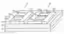
FIG. 1 is a perspective view of the wafer of FIG. 1 having nanowire channels defined thereon at first and second regions;
FIG. 2 is a plan view of a dimension of the nanowire channels of FIG. 1;
FIG. 3 is a perspective view of the wafer of FIG. 1 having reshaped nanowires defined thereon;
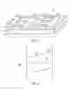
FIG. 4 is a perspective view of a reshaped nanowire having a gate structure; and
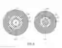
FIG. 5 includes cross-sectional views of nanowires having different thicknesses.
DETAILED DESCRIPTION
Structures to support, for example, gate-all-around (GAA) nanowire field effect transistors (FETs) as well as methods for fabricating the same are provided by way of descriptions referring to silicon (Si) nanowires and Si processing. However, the present techniques can also be practiced with other semiconductor materials such as, for example, germanium (Ge). When non-Si-containing semiconductors are used, the processing steps of the present teachings are similar and adapted to the specific semiconductor used. Use of Si-containing semiconductor materials such as Si, silicon germanium (SiGe), Si/SiGe, silicon carbide (SiC) or silicon germanium carbide (SiGeC) are therefore understood to be merely exemplary.
With reference to FIGS. 1 and 2, a wafer 1 is provided and includes a Si substrate 101, a buried oxide (BOX) layer 102 and a silicon-on-insulator (SOI) layer 103. The wafer 1 can be fabricated using methods such as Separation by IMplanted OXygen (SIMOX) or wafer bonding (for example, SmartCut™). These wafer fabrication techniques are known to those of skill in the art and thus are not described further herein. Also, the substitution of other SOI substrates known in the art for the SOI on BOX configuration described herein may be made and would be within the scope of the present teachings.
The wafer 1 has at least a first region 10 and a second region 20 established thereon. Pairs of SOI pads 103A and nanowire channels 104 connecting them can be patterned into the SOI layer 103 at the first region 10 and the second region 20 to form, for example, ladder-like structures in each region. The patterning of the nanowire channels 104 and SOI pads 103A may be achieved by lithography (e.g., optical or e-beam) followed by reactive ion etching (RIE) or by sidewall transfer techniques. These patterning techniques are known to those of skill in the art.
The SOI layers 103 at the first and second regions 10 and 20 are each initially formed of similar components with similar thicknesses. However, as shown in FIGS. 1 and 2, the SOI pads 103A and the nanowire channels 104 at the first region 10 are formed to have sidewalls that are substantially parallel and/or aligned with, for example, one of the {110} crystallographic planes of the semiconductor, although other planar reference frames are possible. That is, the main (long) axis of each of the nanowire channels 104 is oriented in the direction of the {110} crystallographic planes of the semiconductor. On the other hand, the SOI pads 103A and the nanowire channels 104 at the second region 20 are formed to have sidewalls that are angled and/or misaligned by angle, α, with respect to the {110} crystallographic plane, with the main (long) axis of the nanowires channels 104 also misaligned by angle, α, with respect to the {110} crystallographic plane. For example, nanowires channels 104 in first region 10 can be patterned to have sidewalls parallel to {110} planes and top face parallel to the {100} planes whereas nanowires channels 104 in second region 20 will have sidewalls that are misaligned by an angle, such as α=1 degree, with respect to the {110} crystallographic plane, and top faces that are parallel to the {100} planes.
With the second region 20 nanowire channels 104 angled and/or misaligned, as described above, a thinning operation, such as an anneal of the nanowire channels 104, which is conducted with respect to both the first and the second regions 10 and 20 will tend to have a greater thinning effect at the second region 20 than at the first region 10. This is due to the fact that the offset crystallographic orientation of the SOI layer 103 at the second region 20 leaves the SOI layer 103 at the second region 20 more susceptible to the effects of thinning operations than that of the first region 10. The thinning operation tends to reorient the nanowires channels 104 of the second region 20 to form sidewalls parallel to the {110} crystallographic planes by diffusion of semiconductor material from the nanowire channels 104 to the SOI pads 103A. This has the effect of the nanowire channels 104 in the second region 20 becoming thinner than those at the first region 10 after reorientation.
The degree by which the SOI layer 103 of the second region 20 is thinned more than that of the first region 10 can be controlled by increasing or decreasing relative misalignments of the sidewalls of the first and second regions 10 and 20. For example, the nanowire channel 104 sidewalls at the first region 10 may be aligned with respect to the {110} crystallographic plane of the semiconductor or misaligned by only a small angle, α. Meanwhile, the nanowire channel 104 sidewalls at the second region 20 may be intentionally misaligned with respect to the {110} crystallographic plane of the semiconductor by a relatively large angle, α. Here, the greater the relative misalignments of the sidewalls of the first and second regions 10 and 20, the greater the degree of thinning at the second region 20.
Indeed, with reference to FIG. 2, the angle a of the nanowire channel 104 with respect to the {110} crystallographic plane can be any angle that is less than 45° (and in practice a does not exceed a few degrees) with the understanding that the greater the obliqueness of the angle the more thin the resulting reshaped nanowire 108 will be. That is, a more obliquely angled nanowire channel 104 will tend to form a thinner reshaped nanowire 108 than a more perpendicular nanowire channel 104. Thus, while the dimensions of the nanowire channel 104 and its obliqueness may be varied in accordance with design considerations, a profile of the nanowire channel 104 should encompass at least a profile of the reshaped nanowire 108 that is desired to be formed.
The reorientation process where silicon diffuses from the nanowire channels 104 is described more fully in G. M. Cohen et al., “Controlling the shape and dimensional variability of top-down fabricated silicon nanowires by hydrogen annealing”, Material Research Symposium, San Francisco, Calif., (2010), the contents of which are incorporated herein by reference. The specification for crystal plane directions follows the Miller indices convention, which is described in, e.g., Ashcroft and Mermin, Solid State Physics, chapter 5 (1976), the contents of which are incorporated herein by reference. Following this convention a family of crystal planes, i.e. planes that are equivalent by the virtue of the symmetry of the crystal is typically referenced by a pair of { } parentheses. For example, the planes (100), (010) and (001) are all equivalent in a cubic crystal. One refers to them collectively as {100} planes. When directions in a crystal are referenced [ ] brackets are used, e.g. [100], [010], [001], [−100], [0-10],[00-1], and similarly a family of crystal direction are referred to collectively as <100>.
The nanowire channels 104 at the second region 20 can therefore be formed into reshaped nanowires 108 (see FIG. 3) that are thinner than those of the first region 10 even where an anneal process is conducted in a similar manner at each region. In particular, the reshaped nanowires 108 of the first region 10 will have a thickness T1′ and reshaped nanowires 108 of the second region 20 will have a thickness T2′ that will be different from and generally thinner than the thickness T1′. These differences in the relative thicknesses of the reshaped nanowires 108 at the first and second regions 10 and 20 will, accordingly, lead to the reshaped nanowires 108 exhibiting physical characteristics that may be unique from one another.
The angling of the nanowire channels 104 can be accomplished in various manners. For example, a lithography mask may include as-drawn aligned and misaligned patterns for regions 10 and regions 20, or alternatively during the patterning of the angled nanowire channels 104, the wafer 1 or a patterning mask may be rotated with respect to the {110} crystallographic planes. The angling of the nanowire channels 104 need not be in any particular crystallographic plane, however, and the above-described {110} crystallographic plane is understood to be merely exemplary.
With reference to FIG. 3, the reshaping of the nanowire channels 104 into nanowires 108 is typically accomplished by annealing in an inert gas. This may be a maskless process that is simultaneously or sequentially applied to regions 10 and 20.
As an example, the wafer 1 may be annealed in an exemplary H2 gas. Shortly before this H2 annealing, native oxide may be etched off sidewalls of the nanowire channels 104 and the SOI pads 103A. The annealing in H2 has several goals including, but not limited to, smoothing the sidewalls of the nanowire channels 104, realigning the sidewalls to the crystallographic planes of the SOI pads 103A, re-shaping the nanowire channel 104 cross-sections from rectangular shapes to more cylindrical shapes and thinning of the nanowire channel 104 bodies by way of a re-distribution of Si.
According to an exemplary embodiment, the inert gas anneal is performed with a gas pressure of from about 30 ton to about 1000 torr, at a temperature of from about 600 degrees Celsius (° C.) to about 1100° C. and for a duration of from about one minute to about 120 minutes. In general, the rate of Si re-distribution increases with temperature and decrease with an increase in pressure.
As shown in FIG. 3, the nanowire channels 104 can be reshaped into nanowires 108 and suspended or released from the BOX layer 102 by the annealing process or by a further etching and recessing of the BOX layer 102. The reshaped nanowires 108 thus form suspended bridges between SOI pads 103A and over recessed oxide 105 in the first and second regions 10 and 20. The recessing of the BOX layer 102 can be achieved either as a result of the annealing process or with a diluted hydrofluoric (DHF) etch to undercut the BOX layer 102. While SOI substrates provide an easy path to define and suspend nanowire channels 104 and/or reshaped nanowires 108, it is possible to obtain suspension with other substrates. For example, a SiGe/Si stack epitaxially grown on bulk Si wafers can also be patterned to form the nanowire channels 104 and/or the reshaped nanowires 108. An SiGe layer can also be used as a sacrificial layer (analogous to the BOX layer 102) which is undercut.
The reshaped nanowires 108 at the first region 10 and having a thickness T1′ and the reshaped nanowires 108 at the second region 20 and having a thickness T2′ may have different drive currents and/or threshold voltages. In this way, it is understood that circuit characteristics at least at the first and second regions 10 and 20 of the wafer 1 can be controlled by corresponding control of the angling of the nanowire channels 104 at the first and second regions 10 and 20 which are partially determinative of the final thicknesses T1′ and T2′.
Referring now to FIGS. 4 and 5, a gate structure 402 may be formed around the reshaped nanowires 108. First, the reshaped nanowires 108 are coated with first and second gate dielectrics 112A and 112. The first (and optional) gate dielectric 112A is typically SiO2. The second gate dielectric 112 may include silicon dioxide (SiO2), silicon oxynitride (SiON), hafnium oxide (HfO2) or any other suitable high-k dielectric(s) and may be deposited using chemical vapor deposition (CVD), atomic layer deposition (ALD) or an oxidation furnace in the case of SiO2 and SiON. A conformal deposition of a thin gate conductor 117 of, e.g., TaN or TiN, may then be formed. This may be followed by a deposition of doped poly-Si 113 to form a gate stack 118 perimetrically surrounding the reshaped nanowires 108. A mask 115 is employed to facilitate the etching of a gate line by, for example, RIE. A portion of the thin gate conductor 117 outside of the gate stack 118 may be removed by RIE or, in an alternate embodiment, the removal of the thin gate conductor 117 from surfaces outside gate stack may require an additional wet etch operation.
Poly-germanium or another suitable composition can be used as a substitute to poly-Si 113. Additionally, any poly-SiGe alloy can also be used to substitute poly-Si 113. Still further, poly-Si 113 can be deposited in a poly-crystalline form or deposited in an amorphous form which is later transformed into poly-Si when exposed to high temperature.
While the disclosure has been described with reference to exemplary embodiments, it will be understood by those skilled in the art that various changes may be made and equivalents may be substituted for elements thereof without departing from the scope of the disclosure. In addition, many modifications may be made to adapt a particular situation or material to the teachings of the disclosure without departing from the essential scope thereof. Therefore, it is intended that the disclosure not be limited to the particular exemplary embodiment disclosed as the best mode contemplated for carrying out this disclosure, but that the disclosure will include all embodiments falling within the scope of the appended claims.
Claims
What is claimed is:1. A method of modifying a wafer having a semiconductor disposed on an insulator, the method comprising:
forming first and second nanowire channels connected at each end to semiconductor pads at first and second wafer regions, respectively, with second nanowire channel sidewalls being misaligned relative to a crystallographic plane of the semiconductor to a greater degree than first nanowire channel sidewalls; and
displacing semiconductor material from the first and second nanowire channels toward an alignment condition between the sidewalls thereof and the crystallographic plane such that thickness differences between the first and second nanowire channels after the displacing reflect the greater misalignment of the second nanowire channel sidewalls.
2. The method according to claim 1, wherein the forming comprises forming the nanowire channels of the first region in parallel with one another and forming the nanowire channels of the second region in parallel with one another.
3. The method according to claim 1, wherein the first nanowire channel sidewalls are aligned with respect to the crystallographic plane and the second nanowire channel sidewalls are misaligned with respect to the crystallographic plane.
4. The method according to claim 1, wherein the first and second nanowire channel sidewalls are both misaligned with respect to the crystallographic plane.
5. The method according to claim 1, wherein the displacing of the semiconductor material comprises annealing.
6. The method according to claim 1, further comprising reshaping the nanowire channels into nanowires.
7. The method according to claim 6, further comprising forming a respective gate surrounding each of the nanowires.
8. The method according to claim 7, wherein the gates each comprise a dielectric, a thin gate conductor and doped conductive material.
9. The method according to claim 7, wherein the nanowires each have respective drive currents and/or threshold voltages that differ in accordance with the differences between the thicknesses of the first and second nanowires.
10. The method according to claim 1, wherein the forming comprises a patterning process.
11. A method of modifying a wafer having a semiconductor disposed on an insulator, the method comprising:
forming first and second nanowire channels connected at each end to semiconductor pads at first and second wafer regions, respectively, with first nanowire channel sidewalls characterized with a first alignment degree relative to a crystallographic plane of the semiconductor and second nanowire channel sidewalls characterized with a second alignment degree relative to the crystallographic plane, which is different from the first alignment degree; and
encouraging displacement of semiconductor material from the first and second nanowire channels toward an alignment condition between the sidewalls and the crystallographic plane such that thickness differences between the first and second nanowire channels after the displacement are in accordance with the first and second alignment degree difference.
12. A method of modifying a wafer having a semiconductor disposed on an insulator, the method comprising:
forming, in a first region of the wafer, pairs of semiconductor pads connected by nanowire channels having long axes thereof oriented in the {110} crystallographic planes of the semiconductor and sidewalls substantially parallel to one of the {110} planes of the semiconductor;
forming, in a second region of the wafer, pairs of semiconductor pads connected by nanowire channels having long axes thereof at an angle with respect to the {110} crystallographic planes of the semiconductor and sidewalls similarly angled with respect to the {110} planes of the semiconductor; and
reorienting the nanowires channels of the second region to form sidewalls parallel to the {110} planes of the semiconductor by diffusion of semiconductor material from the nanowires channels to the pads such that the nanowire channels in the second region are thinned as compared to those at the first region.
13. The method according to claim 12, further comprising reshaping the nanowire channels into nanowires.
14. The method according to claim 13, further comprising forming a respective gate surrounding each of the nanowires.
15. The method according to claim 14, wherein the gates each comprise a dielectric, a thin gate conductor and doped conductive material.
16. The method according to claim 14, wherein the nanowires each have respective drive currents and/or threshold voltages that differ in accordance with the differences between the thicknesses of the first and second nanowires.
17. The method according to claim 12, wherein the forming comprises a patterning process
18. A wafer, comprising:
a substrate;
a buried oxide (BOX) layer disposed on the substrate; and
a silicon-on-insulator (SOI) structure disposed on the BOX layer at first and second regions, the SOI structure at each region having respective pairs of SOI pads connected via respective nanowire channels formed therein,
the SOI pads and the nanowire channels at one of the regions being more misaligned with respect to {110} planes of the SOI than the SOI pads and the nanowire channels at the other of the regions.
19. The wafer according to claim 18, wherein a profile of the misaligned nanowire channels encompasses a reshaped nanowire formable therefrom.
20. The wafer according to claim 18, wherein the nanowire channels are parallel with one another at each of the first and second regions, respectively.
Images & Drawings included:

Sources:
- United States Patent and Trademark Office - verify current appl. status at the USPTO↗
Similar patent applications:
- » 20110278543
Generation of multiple diameter nanowire field effect transistors - » 20110278544
Generation of multiple diameter nanowire field effect transistors - » 20130001517
Generation of multiple diameter nanowire field effect transistors - » 20130017673
Generation of multiple diameter nanowire field effect transistors - » 20140239254
GENERATION OF MULTIPLE DIAMETER NANOWIRE FIELD EFFECT TRANSISTORS
Recent applications in this class:
- » 20250063778 2025-02-20
GATE STRUCTURE IN SEMICONDUCTOR METHOD AND METHOD OF FORMING THE SAME - » 20240421185 2024-12-19
CONVERGENT FIN AND NANOSTRUCTURE TRANSISTOR STRUCTURE AND METHOD - » 20240405070 2024-12-05
TRANSISTOR SOURCE/DRAIN REGIONS - » 20240405069 2024-12-05
THROUGH-SUBSTRATE VIA AND METHOD FOR FORMING THE SAME - » 20240395860 2024-11-28
SEMICONDUCTOR DEVICE STRUCTURE WITH GATE STACK - » 20240395859 2024-11-28
INTEGRATED CIRCUIT WITH NANOSTRUCTURE TRANSISTORS AND BOTTOM DIELECTRIC INSULATORS - » 20240395858 2024-11-28
SEMICONDUCTOR DEVICES AND METHODS OF MANUFACTURING THEREOF - » 20240395857 2024-11-28
SEMICONDUCTOR DEVICE WITH WRAP AROUND SILICIDE LAYER - » 20240395856 2024-11-28
SEMICONDUCTOR DEVICE STRUCTURE AND METHODS OF FORMING THE SAME - » 20240387630 2024-11-21
INTEGRATED CIRCUIT STRUCTURE AND METHOD FOR FORMING THE SAME
Recent applications for this Assignee:
- » 20250294045 2025-09-18
THREAT POLICY FINE-TUNING BASED ON THE VULNERABILITY OF A SUBNET AS A SOURCE OF A MALICIOUS ATTACK - » 20250294041 2025-09-18
DEVICE POPULATION ANOMALY DETECTION - » 20250292574 2025-09-18
SCENE PARSING - » 20250292026 2025-09-18
A GENERATIVE ARTIFICIAL INTELLIGENCE COMMENTARY - » 20250291689 2025-09-18
MACHINE LEARNING MODEL TRAINING TO ASSIST IN SYSTEM DEBUG - » 20250287215 2025-09-11
PORTABLE MEDIA GEOFENCE AND DEVICE PAIRING SECURITY - » 20250285610 2025-09-11
RECIPIENT-SPECIFIC VOICE TONE ADJUSTMENT IN TELEPHONY - » 20250284728 2025-09-11
CONTEXT LARGE LANGUAGE MODEL OUTPUT EXPLANATION - » 20250278669 2025-09-04
COUNTERFACTUALS WITH FEATURE PREFERENCES FOR CONSISTENT AND DIVERSE EXPLANATIONS - » 20250274345 2025-08-28
MULTI-LAYER EDGE ARCHITECTURE SIMULATION