Enclosure of electronic device
US20110297413A1
2011-12-08
12/860,941
2010-08-23
✅ Patent granted
US 8,350,150 B2
2013-01-08
-
-
Dhirubhai R Patel
2031-06-24
Abstract:
An enclosure of an electronic device includes a plate. The plate defines a number of through holes. Each through hole has a pair of tabs connected to each other and with the through hole. Each pair of tabs are slantingly bent towards an inside of the enclosure. The enclosure with the shields can shield the electronic device from electro-magnetic interference.
Inventors:
- PO-CHUAN HSIEH 33 🇹🇼 Tu-Cheng, Taiwan
- CHIEN-HUNG LIU 36 🇹🇼 Tu-Cheng, Taiwan
- YU-CHANG PAI 63 🇹🇼 Tu-Cheng, Taiwan
- Chien-Hung Liu 25 🇹🇼 Taipei Hsien, Taiwan
- YU-CHANG PAI 32 🇹🇼 Taipei Hsien, Taiwan
- Po-Chuan Hsieh 15 🇹🇼 Taipei Hsien, Taiwan
Assignee:
- HON HAI PRECISION INDUSTRY CO., LTD. 12,833 🇹🇼 Tu-Cheng, Taiwan
- HON HAI PRECISION INDUSTRY CO., LTD. 10,014 🇹🇼 New Taipei, Taiwan
Interested in similar patents?
Get notified when new applications in this technology area are published.
Classification:
H05K9/0041 » CPC main
Screening of apparatus or components against electric or magnetic fields; Casings Ventilation panels having provisions for screening
H05K9/0041 » CPC main
Screening of apparatus or components against electric or magnetic fields; Casings Ventilation panels having provisions for screening
B21D28/10 » CPC further
Shaping by press-cutting; Perforating; Punching blanks or articles with or without obtaining scrap ; Notching Incompletely punching in such a manner that the parts are still coherent with the work
Y10T29/49 » CPC further
Metal working Method of mechanical manufacture
Y10T29/49826 » CPC further
Metal working; Method of mechanical manufacture Assembling or joining
H05K7/00 IPC
Constructional details common to different types of electric apparatus
H05K7/00 IPC
Constructional details common to different types of electric apparatus
B23P19/04 IPC
Machines for simply fitting together or separating metal parts or objects, or metal and non-metal parts, whether or not involving some deformation ; Tools or devices therefor so far as not provided for in other classes for assembling or disassembling parts
B23P17/00 IPC
Metal-working operations, not covered by a single other subclass or another group in this subclass
H05K5/00 IPC
Casings, cabinets or drawers for electric apparatus
H05K5/00 IPC
Casings, cabinets or drawers for electric apparatus
Description
CROSS-REFERENCE TO RELATED APPLICATIONS
Relevant subject matter is disclosed in the co-pending U.S. patent applications (Attorney Docket Nos. US32221, US32384, US32670, US32671, US32875, and US33505) having the same title and assigned to the same assignee as named herein.
BACKGROUND
1. Technical Field
The present disclosure relates to an enclosure of an electronic device.
2. Description of Related Art
For the enclosure of a typical electronic device, electromagnetic interference
(EMI) is a common problem during operation. Commonly, through holes are defined in the enclosure for aiding in heat dissipation, and though sizes and placement of the holes are chosen and arranged to help avoid EMI, problems from EMI still occur.
BRIEF DESCRIPTION OF THE DRAWINGS
Many aspects of the embodiments can be better understood with reference to the following drawings. The components in the drawings are not necessarily drawn to scale, the emphasis instead being placed upon clearly illustrating the principles of the present embodiments. Moreover, in the drawings, like reference numerals designate corresponding parts throughout the several views.
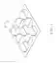
FIG. 1 is an isometric view of a plate in an exemplary embodiment of enclosure of an electronic device.
FIG. 2 is a side view of the plate of FIG. 1.
FIG. 3 is a graph showing EMI shielding effectiveness of a conventional enclosure and an enclosure using the plate of FIG. 1.
FIG. 4 is a flowchart of an exemplary embodiment of a manufacturing method for the plate of FIG. 1.
DETAILED DESCRIPTION
The disclosure, including the accompanying drawings, is illustrated by way of example and not by way of limitation. It should be noted that references to “an” or “one” embodiment in this disclosure are not necessarily to the same embodiment, and such references mean at least one.
Referring to FIGS. 1 to 3, an exemplary embodiment of an enclosure of an electronic device includes a plate 2. The plate 2 can be arranged on a front side or a back side of the enclosure.
The plate 2 is quadrate shaped. A plurality of pairs of tabs 40 and 42 are punched in the plate 2. Each pair of tabs includes one tab 40 and one tab 42. Each tab is substantially semicircular, and straight sides of the two tabs are connected together. Each pair of tabs 40 and 42 are slantingly bent towards an inside of the enclosure. As a result, a plurality of through holes 3 is formed in the plate 2. Heat inside the enclosure can be vented to the outside through the through holes 3.
From another perspective, the plate 2 defines a plurality of through holes 3, with a plurality of shields 4 partly covering the through holes 3. Each through hole 3 is a round hole. Each shield 4 includes a first tab 40 and a second tab 42 connected to the first tab 40. Each of the first tab 40 and the second tab 42 is substantially semicircular, and has a same radius as the corresponding through hole 3. The first tab 40 and the second tab 42 are connected together at the straight sides of the first and second tabs 40 and 42, with the first and second tabs 40 and 42 angled. The straight sides of the first and second tabs 40 and 42 in every two adjacent through holes 3 are not parallel. In this embodiment, the straight sides of the first and second tabs 40 and 42 in every two adjacent through holes 3 are perpendicular to each other. As a result, heat inside the enclosure can be vented to the outside through the through holes 3.
Referring to FIG. 3, a curve A1 represents EMI shielding effectiveness of a conventional enclosure. A curve A2 represents EMI shielding effectiveness of the enclosure with the plate 2 of FIG. 1. FIG. 3 clearly indicates that the EMI shielding effectiveness of the enclosure with the plate 2 is better than the EMI shielding effectiveness of the conventional enclosure.
Furthermore, in other embodiments, the size and shape of the first tab 40 and the second tab 42 of the shield 4 can be changed according to need. When the shields 4 are configured with a different size and a different shape, the EMI shielding effectiveness of the enclosure may be different. In addition, shape of the through holes 3 need not be round as shown in the figures. Furthermore, in other embodiments, the first tab 40 and the second tab 42 can be pivotably coupled together, thus to change an angle between the first tab 40 and the second tab 42. When the first tab 40 and the second tab 42 have different angle, the EMI shielding effectiveness of the enclosure may be different.
Referring to FIG. 4, an exemplary embodiment of a manufacturing method for the plate 2 includes the following steps.
In step S1, a plurality of pairs of tabs is punched in a plate. Each pair of tabs includes two opposite tabs, and each tab is substantially semicircular and straight sides of the pair of tabs are connected together. In one embodiment, the straight sides of adjacent pairs of tabs are made not parallel to each other.
In step S2, each pair of tabs are slantingly bent towards an inside of the enclosure to form the shields 4 and the through holes 3.
The foregoing description of the embodiments of the disclosure has been presented only for the purposes of illustration and description and is not intended to be exhaustive or to limit the disclosure to the precise forms disclosed. Many modifications and variations are possible in light of the above everything. The embodiments were chosen and described in order to explain the principles of the disclosure and their practical application so as to enable others of ordinary skill in the art to utilize the disclosure and various embodiments and with various modifications as are suited to the particular use contemplated. Alternative embodiments will become apparent to those of ordinary skills in the art to which the present disclosure pertains without departing from its spirit and scope. Accordingly, the scope of the present disclosure is defined by the appended claims rather than the foregoing description and the exemplary embodiments described therein.
Claims
What is claimed is:1. An enclosure of an electronic device, the enclosure comprising a plate, wherein the plate defines a plurality of through holes, each through hole has a pair of tabs connected to each other and with the through hole, and each pair of tabs are slantingly bent towards an inside of the enclosure.
2. The enclosure of claim 1, wherein each through hole is a round hole, each tab is substantially semicircular and has a same radius as the through hole.
3. The enclosure of claim 2, wherein each pair of tabs are connected via a shared straight side, the straight sides of the tabs in every two adjacent through holes are nonparallel.
4. The enclosure of claim 3, wherein the straight sides of the tabs in every two adjacent through holes are perpendicular to each other.
5. The enclosure of claim 1, wherein the two tabs are pivotably coupled together.
6. A manufacturing method for a plate, the manufacturing method comprising:
punching a plurality of pairs of tabs in the plate; and
slantingly and bending each pair of tabs to form a plurality of shields and a plurality of through holes.
7. The manufacturing method of claim 6, wherein each pair of tabs are substantially semicircular.
8. The manufacturing method of claim 6, wherein each pair of tabs is connected via a shared straight side, the straight sides of the tabs in every two adjacent through holes are nonparallel.
9. The manufacturing method of claim 8, wherein the straight sides of the tabs in every two adjacent through holes are perpendicular to each other.
Images & Drawings included:


Sources:
- United States Patent and Trademark Office - verify current appl. status at the USPTO↗
Similar patent applications:
- » 20110164378
Electronic device enclosure and electronic device - » 20150351265
Electronic device enclosure and electronic device - » 16564244
Electronic device enclosure having a textured glass component - » 20050164525
Electronic device enclosure with rotationally locked body and header - » 10899576
Method and apparatus for controlling the temperature of electronic device enclosures - » 15260902
Vehicle mounted electronic device enclosure - » 10932724
Cover assembly for an electronic device enclosure - » 14584800
Antenna tile arrangements in electronic device enclosures - » 14041453
Electronic device enclosure assembly - » 20050007747
Metal electronics device enclosure
Recent applications in this class:
- » 20250203828 2025-06-19
REDUCTION OF RADIATED EMISSIONS USING SPARSE MESH ADDITIVE MATERIAL - » 20250056774 2025-02-13
SYSTEM AND METHOD FOR MANAGING ELECTROMAGNETIC INTERFERENCE - » 20240268089 2024-08-08
SYSTEM AND METHOD FOR THERMAL MANAGEMENT AND ELECTROMAGNETIC INTERFERENCE MANAGEMENT - » 20230156983 2023-05-18
AIR-VENT WITH NON-UNIFORM CROSS SECTION FOR EMI SHIELDING - » 20230008116 2023-01-12
Air vent with openings of non-uniform size and location for improved EMI shielding - » 20220183195 2022-06-09
SYSTEM AND METHOD FOR MANAGING ELECTROMAGNETIC INTERFERENCE - » 20210315136 2021-10-07
Air duct with EMI suppression - » 20210022275 2021-01-21
System and method for thermal management and electromagnetic interference management - » 20180249600 2018-08-30
Smart EMI vent - » 20180132389 2018-05-10
Arrangement for protecting electronics from interference radiation
Recent applications for this Assignee:
- » 20250218287 2025-07-03
METHOD OF GENERATING AND PROMPTING TRAFFIC INFORMATION, AND ROADSIDE DEVICE THEREOF - » 20250178535 2025-06-05
METHOD FOR CONSTRUCTING 3D PANORAMIC VIEW MODEL, VEHICLE-MOUNTED DEVICE, AND STORAGE MEDIUM - » 20250074444 2025-03-06
METHOD FOR EARLY WARNING A BLIND AREA, ELECTRONIC DEVICE AND STORAGE MEDIUM - » 20240416754 2024-12-19
DISPLAY CONTROL DEVICE, DISPLAY EQUIPMENT, AND VEHICLE EMPLOYING DEVICE - » 20240411051 2024-12-12
Light-emitting device array and optical transceiver system having the same - » 20240324114 2024-09-26
DISPLAY CONTROL DEVICE AND VEHICLE EMPLOYING DEVICE - » 20240295957 2024-09-05
METHOD FOR CONTROLLING ELECTRONIC DEVICE, ELECTRONIC DEVICE AND COMPUTER STROAGE MEDIUM EMPLOYING METHOD - » 20240257357 2024-08-01
METHOD FOR DETECTING OBSTACLES, ELECTRONIC DEVICE, AND STORAGE MEDIUM - » 20240203133 2024-06-20
LANE LINE RECOGNITION METHOD, ELECTRONIC DEVICE AND STORAGE MEDIUM - » 20240194999 2024-06-13
Robot using limiting device for locking battery