Forming an electrode having reduced corrosion and water decomposition on surface using an organic protective layer
US20110312176A1
2011-12-22
12/820,543
2010-06-22
✅ Patent granted
US 8,354,336 B2
2013-01-15
-
-
Julio J Maldonado | Shantanu C Pathak
Cantor Colburn LLP | Vazken Alexanian
2030-06-22
Abstract:
Accordingly, the present invention provides a method of forming an electrode having reduced corrosion and water decomposition on a surface thereof. A substrate which has a conductive layer disposed thereon is provided and the conductive layer has an oxide layer with an exposed surface. The exposed surface of the oxide layer contacts a solution of an organic surface active compound in an organic solvent to form a protective layer of the organic surface active compound over the oxide layer. The protective layer has a thickness of from about 0.5 nm to about 5 nm and ranges therebetween depending on a chemical structure of the surface active compound.
Inventors:
- Ali Afzali-Ardakani 200 🇺🇸 Ossining, NY, United States
- Glenn J. Martyna 46 🇺🇸 Croton on Hudson, NY, United States
- Hongbo Peng 29 🇺🇸 Chappaqua, NY, United States
- Gustavo A. Stolovitzky 71 🇺🇸 Riverdale, NY, United States
- Hariklia Deligianni 91 🇺🇸 Tenafly, NJ, United States
- Xiaoyan Shao 48 🇺🇸 Yorktown Heights, NY, United States
- Shafaat Ahmed 20 🇺🇸 Yorktown Heights, NY, United States
- Stephen Rossnagel 12 🇺🇸 Pleasantville, NY, United States
- Dario L. Goldfarb 27 🇺🇸 Dobbs Ferry, NY, United States
- Stanislav Polonsky 54 🇺🇸 Putnam Valley, NY, United States
- Binquan Luan 11 🇺🇸 Ossining, NY, United States
- Stefan Harrer 18 🇺🇸 New York, NY, United States
- Hongbo Peng 3 🇺🇸 , United States
- Stanislav Polonsky 3 🇺🇸 , United States
- Stephen Rossnagel 3 🇺🇸 , United States
Assignee:
- INTERNATIONAL BUSINESS MACHINES CORPORATION 136,239 🇺🇸 ARMONK, NY, United States
Applicant:
Interested in similar patents?
Get notified when new applications in this technology area are published.
Classification:
H01L21/3205 IPC
Processes or apparatus adapted for the manufacture or treatment of semiconductor or solid state devices or of parts thereof; Manufacture or treatment of semiconductor devices or of parts thereof the devices having at least one potential-jump barrier or surface barrier, e.g. PN junction, depletion layer or carrier concentration layer the devices having semiconductor bodies comprising elements of Group IV of the Periodic System or AB compounds with or without impurities, e.g. doping materials; Treatment of semiconductor bodies using processes or apparatus not provided for in groups - to form insulating layers thereon, e.g. for masking or by using photolithographic techniques ; After treatment of these layers; Selection of materials for these layers Deposition of non-insulating-, e.g. conductive- or resistive-, layers on insulating layers; After-treatment of these layers
B82Y10/00 » CPC main
Nanotechnology for information processing, storage or transmission, e.g. quantum computing or single electron logic
H01L51/102 » CPC further
Solid state devices using organic materials as the active part, or using a combination of organic materials with other materials as the active part; Processes or apparatus specially adapted for the manufacture or treatment of such devices, or of parts thereof specially adapted for rectifying, amplifying, oscillating or switching, or capacitors or resistors with at least one potential- jump barrier or surface barrier multistep processes for their manufacture; Details of devices Electrodes
H01L21/76834 » CPC further
Processes or apparatus adapted for the manufacture or treatment of semiconductor or solid state devices or of parts thereof; Manufacture or treatment of devices consisting of a plurality of solid state components formed in or on a common substrate or of parts thereof; Manufacture of integrated circuit devices or of parts thereof; Manufacture of specific parts of devices defined in group; Applying interconnections to be used for carrying current between separate components within a device comprising conductors and dielectrics characterised by the formation and the after-treatment of the dielectrics, e.g. smoothing characterised by the formation of thin functional dielectric layers, e.g. dielectric etch-stop, barrier, capping or liner layers formation of thin insulating films on the sidewalls or on top of conductors
H01L29/0665 » CPC further
Semiconductor devices adapted for rectifying, amplifying, oscillating or switching, or capacitors or resistors with at least one potential-jump barrier or surface barrier, e.g. PN junction depletion layer or carrier concentration layer; Details of semiconductor bodies or of electrodes thereof; Multistep manufacturing processes therefor; Semiconductor bodies ; Multistep manufacturing processes therefor characterised by their shape; characterised by the shapes, relative sizes, or dispositions of the semiconductor regions ; characterised by the concentration or distribution of impurities within semiconductor regions characterised by the shape of the body the shape of the body defining a nanostructure
H01L51/0093 » CPC further
Solid state devices using organic materials as the active part, or using a combination of organic materials with other materials as the active part; Processes or apparatus specially adapted for the manufacture or treatment of such devices, or of parts thereof; Selection of organic semiconducting materials, e.g. organic light sensitive or organic light emitting materials Biomolecules or bio-macromolecules, e.g. proteines, ATP, chlorophyl, beta-carotene, lipids, enzymes
H01L51/0504 » CPC further
Solid state devices using organic materials as the active part, or using a combination of organic materials with other materials as the active part; Processes or apparatus specially adapted for the manufacture or treatment of such devices, or of parts thereof specially adapted for rectifying, amplifying, oscillating or switching, or capacitors or resistors with at least one potential- jump barrier or surface barrier multistep processes for their manufacture the devices being controllable only by the electric current supplied or the electric potential applied, to an electrode which does not carry the current to be rectified, amplified or swiched, e.g. three-terminal devices
H01L21/283 IPC
Processes or apparatus adapted for the manufacture or treatment of semiconductor or solid state devices or of parts thereof; Manufacture or treatment of semiconductor devices or of parts thereof the devices having at least one potential-jump barrier or surface barrier, e.g. PN junction, depletion layer or carrier concentration layer the devices having semiconductor bodies comprising elements of Group IV of the Periodic System or AB compounds with or without impurities, e.g. doping materials; Manufacture of electrodes on semiconductor bodies using processes or apparatus not provided for in groups - Deposition of conductive or insulating materials for electrodes conducting electric current
H01L21/441 IPC
Processes or apparatus adapted for the manufacture or treatment of semiconductor or solid state devices or of parts thereof; Manufacture or treatment of semiconductor devices or of parts thereof the devices having at least one potential-jump barrier or surface barrier, e.g. PN junction, depletion layer or carrier concentration layer the devices having semiconductor bodies not provided for in groups, , , and with or without impurities, e.g. doping materials; Manufacture of electrodes on semiconductor bodies using processes or apparatus not provided for in groups - Deposition of conductive or insulating materials for electrodes
C23C28/00 IPC
Coating for obtaining at least two superposed coatings either by methods not provided for in a single one of groups - or by combinations of methods provided for in subclasses and or
C30B23/02 IPC
Single-crystal growth by condensing evaporated or sublimed materials Epitaxial-layer growth
C23C14/34 IPC
Coating by vacuum evaporation, by sputtering or by ion implantation of the coating forming material characterised by the process of coating Sputtering
B05D3/14 IPC
Pretreatment of surfaces to which liquids or other fluent materials are to be applied; After-treatment of applied coatings, e.g. intermediate treating of an applied coating preparatory to subsequent applications of liquids or other fluent materials by electrical means
B05D5/12 IPC
Processes for applying liquids or other fluent materials to surfaces to obtain special surface effects, finishes or structures to obtain a coating with specific electrical properties
B05D3/06 IPC
Pretreatment of surfaces to which liquids or other fluent materials are to be applied; After-treatment of applied coatings, e.g. intermediate treating of an applied coating preparatory to subsequent applications of liquids or other fluent materials by exposure to radiation
H01L21/28 IPC
Processes or apparatus adapted for the manufacture or treatment of semiconductor or solid state devices or of parts thereof; Manufacture or treatment of semiconductor devices or of parts thereof the devices having at least one potential-jump barrier or surface barrier, e.g. PN junction, depletion layer or carrier concentration layer the devices having semiconductor bodies comprising elements of Group IV of the Periodic System or AB compounds with or without impurities, e.g. doping materials Manufacture of electrodes on semiconductor bodies using processes or apparatus not provided for in groups -
Description
CROSS-REFERENCE TO RELATED APPLICATIONS
This application is related to U.S. Patent Application 20080187915 filed Feb. 2, 2002, U.S. Patent Application 2010025249 filed Aug. 13, 2009, IBM Docket Number YOR920100340US1 entitled “FORMING AN ELECTRODE HAVING REDUCED CORROSION AND WATER DECOMPOSTION ON SURFACE USING A CUSTOM OXIDE LAYER” filed on ______ having Ser. No. ______, IBM Docket Number YOR920100342US1 entitled “REDUCING CORROSION AND WATER DECOMPOSITION ON A SURFACE OF A TITANIUM NITRIDE ELECTRODE” filed on ______ having Ser. No. ______, all incorporate herein by reference.
BACKGROUND OF THE INVENTION
The field of the present invention relates generally to thin film electrodes and, more particularly, to forming an electrode having reduced corrosion and water decomposition on the surface of the electrode.
Electrochemical corrosion of an electrode causes deterioration of the electrode and reduced functionality. Further, if the electrode is immersed in an aqueous solution and a voltage is applied, then water decomposes forming oxygen and hydrogen bubbles on the surface of an electrode.
Protecting surfaces against corrosion by coating such surfaces with an inert substance is known. The protective coating can be a layer of a metal with better protection properties than the bulk material, for example, covering iron or unalloyed steal with a layer of treated zinc. A second option is the protective coating can be an enamel layer or glass-like layer of an inorganic non-metallic material. The third option for corrosion protection is coating with an organic polymer, for example, intrinsically conducting polymers. There is a need for an improved method of inhibiting electrochemical corrosion and water decomposition on electrode surfaces.
BRIEF SUMMARY OF THE INVENTION
Accordingly, the present invention provides a method of forming an electrode having reduced corrosion and water decomposition on a surface thereof. A substrate which has a conductive layer disposed thereon is provided and the conductive layer has an oxide layer with an exposed surface. The exposed surface of the oxide layer contacts a solution of an organic surface active compound in an organic solvent to form a protective layer of the organic surface active compound over the oxide layer. The protective layer has a thickness of from about 0.5 nm to about 5 nm and ranges therebetween depending on a chemical structure of the surface active compound.
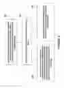
BRIEF DESCRIPTION OF THE SEVERAL VIEWS OF THE DRAWINGS
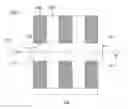
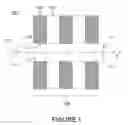
FIG. 1 shows a diagram of a DNA-Transistor device.
FIG. 2 shows a flow chart for a method of forming an electrode having reduced corrosion and water decomposition on a surface thereof according to an embodiment of the present invention.
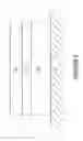
FIG. 3 shows a diagram of the electrode formed as a result of the method of an embodiment of the present invention.
FIG. 4 shows a flow chart for a method of inhibiting corrosion and water decomposition on an electrode surface according to an embodiment of the present invention.
DETAILED DESCRIPTION OF THE INVENTION
Thin film electrodes are used in the emerging technology of DNA-Transistors. For a detailed explanation of DNA-Transistors see U.S. Patent Application 20080187915 and U.S. Patent Application 2010025249, both incorporated herein by reference.
FIG. 1 shows a diagram of a DNA-Transistor device 100. The device 100 is capable of controlling the position of a DNA molecule 101 inside a nanopore 102 with single nucleotide accuracy. The device uses the interaction of charges 103 along the backbone of a DNA molecule 101 with an electric field created inside the nanopore 102. The nanopore 102 is drilled through a rack structure 104 of conductive layers 105 and dielectric layers 106 and then wetted with a solvent-electrolyte solution 107 carrying the DNA molecules 101. The surface areas of the conductive layers that are exposed to the solution 107 inside the nanopore 102 serve as electrodes 108 for generating and controlling the electric fields inside the nanopore 102. Voltages applied to the conductive layers 105 in the rack structure 104 allow for trapping and moving the DNA molecule 101 in the nanopore 102.
It is essential for maintaining functionality of the DNA-Transistor device 100 that the nanopore 102 dimensions are not spatially altered and continuous solution 107 flow inside the pore is not compromised during device operation. Specifically, this means that corrosion of the electrode 108 surface areas inside the nanopore 102 must be reduced and water decomposition catalyzed on the surface areas of electrodes 108 must be reduced.
FIG. 2 shows a flow chart for a method 200 of forming an electrode having reduced corrosion and water decomposition on a surface thereof according to an embodiment of the present invention. In step 201 a substrate having a conductive layer disposed thereon is provided, wherein the conductive layer has an oxide layer with an exposed surface. In step 202 the exposed surface of the oxide layer contacts a solution containing an organic surface active compound in an organic solvent to form a protective layer of the organic surface active compound over the oxide layer.
FIG. 3 shows a diagram of the electrode formed as a result of the method of an embodiment of the present invention. The substrate 301 serves as the medium onto which the conductive layer 302 is deposited. An oxide layer 303 is formed on the conductive layer 302. A protective layer 304 of organic surface active compound is formed over the oxide layer 303.
The substrate 301 can be any type of common substrate material such as Kapton, silicon, amorphous hydrogenated silicon, silicon carbide (SiC), silicon dioxide (SiO2), quartz, sapphire, glass, metal, diamond-like carbon, hydrogenated diamond-like carbon, gallium nitride, gallium arsenide, germanium, silicon-germanium, indium tin oxide, boron carbide, boron nitride, silicon nitride (Si3N4), alumina (Al2O3), cerium(IV) oxide (CeO2), tin oxide (SnO2), zinc titanate (ZnTiO2), AlGaAs, CN, InP, GaP, In0.53Ga0.47As, chalcogenides, a plastic material and a combination thereof.
The conductive layer 302 can be a metal, semiconductor or a doped semiconductor. Preferably, the conductive layer is titanium nitride; however, other conductive materials can be used. The conductive layer 302 can be a metal such as platinum, rhodium, gold, silver, zinc, titanium, ruthenium and aluminum. The conductive layer 302 can be a semiconductor such as GaAs, AlGaAs, NC, Ge, SiGe, InP, GaP, GaN, In0.53Ga0.47As and chalcogenides. The chalcogenide can be a compound of a metal such as Ge, Sn, Pb, Sb, Bi, Ga, In, TI and a combination thereof and a chalcogen such as S, Se, Te and a combination thereof. The conductive layer 105 can also be a doped semiconductor such as aluminum doped zinc oxide, phosphorus doped silicon, boron doped silicon, lanthanum doped zirconium dioxide, scandium doped zirconium dioxide, and yttrium doped zirconium dioxide. The conductive layer 302 can be deposited by any deposition process such as sputtering, molecular beam epitaxy, ion beam lithography and atomic layer deposition.
The oxide layer 303 can be formed through any known method of oxidation; however, preferably the oxidation is carried out by plasma oxidation in order to create an ultra-thin oxide layer 303. A preferred custom oxygen plasma process uses a working pressure of 150 mT, an oxygen flow rate of 100 sccm, a power of 40-200 W and a time of 0-80 seconds. The custom process provides a uniform oxide layer 303 free of surface defects. The thickness of the oxide layer 303 can be reduced to a thickness of 0.09 nm with a precision of 0.2 nm. It is beneficial that the oxide layer 303 be ultra-thin and highly uniform in application inside a nanopore. The custom oxygen plasma process can be applied not only to planar surfaces but also to topographically patterned surfaces isotropically oxidizing angled and vertical sidewalls as found inside a nanopore.
The protective layer 304 is formed by self assembly of an organic surface active compound. The organic surface active compound has a structure which includes a polar end and a non-polar end. The polar end of the organic surface active compound forms a hydrogen bond with oxygen of the oxide layer 303 and the non-polar end forms the protective layer 304.
Preferably the protective layer 304 is a highly compact self assembled monolayer of a long chain organic phosphonic acid or hydroxamic acid. More specifically, the preferred organic surface active compound is represented by the formula:
R—(CH2)n—XH
wherein R is an alkyl group of 1-4 carbon atoms; n is from 0 to about 18; and —XH is a moiety selected from the group consisting of: —CONHOH, —COOH, —SO2OH, —SOON, —SO2NHOH, —P(O)2NHOH, —P(O)2OH, —PO3H, and mixtures thereof. The alkyl chains of phosphnoic or hyroxamic acids can also be partically or fully fluorinated to impart yet higher hydrophobicity on the exposed surface.
FIG. 4 shows a flow chart for a method of inhibiting corrosion and water decomposition on an electrode surface according to an embodiment of the present invention.
In step 401 the electrode is immersed in a solvent having an electrolyte dissolved therein. Preferably, the solvent is an organic solvent such as methanol, ethanol, propanol, butanol, ethylene glycol, ethyl acetate, 1,2-propanediol, 1,3-propanediol, diethyl ether, methyl ethyl ketone, methoxyethyl acetate, methoxypropyl acetate, methylene chloride, acetone, aliphatic hydrocarbons, aromatic hydrocarbons, and mixtures thereof.
In order to inhibit corrosion and water decomposition, the solvent contains a hydroxyl-functional compound such as a linear, branched, or cyclic alcohol of 1 to 6 carbon atoms, ethylene glycol, propylene glycol, butane diol, pentane diol, hexan diol, polyethylene glycol, glycerol, trimethylol ethane, trimethylol propane, isomers thereof, aqueous solutions thereof, and mixtures any of the preceding hydroxyl-functional compounds. Preferably, the solution containing hydroxyl-functional compound has a viscosity from about 1 centi Stokes (cSt) to about 250 centi Stokes.
Further, preferably the solvent also contains a solubility promoter such as dimethylsulfoxide, N,N-dimethylformaide, N,N-dimethylacetamaide, tri(dimethylamino)phosphine, tri(dimethylamino)phosphoramide, ethyl acetate, diethyl ether, methyl ethyl ketone, methoxyethyl acetate, methoxypropyl acetate, methylene chloride, acetone, and mixtures thereof.
The electrolyte dissolved in the solvent can be a salt, an ammonium salt, a quaternary ammonium salt, a substantially dissociated compound, ionic liquids, and mixtures thereof. The electrolyte is preferably at a concentration from about 0.001 weight percent to about 10 weight percent.
In step 402 a voltage is applied to the conductive layer to induce a current therein. The current can be either AC or DC current.
In step 403 the extent of oxidation of the conductive layer is measured. Preferably, this is carried out by using cross-sectional transmission electron microscopy, cross-section scanning electron microscopy and/or using a top view atomic force microscopy.
In step 404 the extent of water decomposition is measured by visually observing the formation of hydrogen and oxygen bubbles.
The terminology used herein is for the purpose of describing particular embodiments only and is not intended to be limiting of the invention. As used herein, the singular forms “a”, “an” and “the” are intended to include the plural forms as well, unless the context clearly indicates otherwise. It will be further understood that the terms “comprises” and/or “comprising,” when used in this specification, specify the presence of stated features, integers, steps, operations, elements, and/or components, but do not preclude the presence or addition of one or more other features, integers, steps, operations, elements, components, and/or groups thereof.
The corresponding structures, materials, acts, and equivalents of all means or step plus function elements in the claims below are intended to include any structure, material, or act for performing the function in combination with other claimed elements as specifically claimed. The description of the present invention has been presented for purposes of illustration and description, but is not intended to be exhaustive or limited to the invention in the form disclosed. Many modifications and variations will be apparent to those of ordinary skill in the art without departing from the scope and spirit of the invention. The embodiment was chosen and described in order to best explain the principles of the invention and the practical application, and to enable others of ordinary skill in the art to understand the invention for various embodiments with various modifications as are suited to the particular use contemplated.
Claims
1. A method of forming an electrode having reduced corrosion and water decomposition on a surface thereof, the method comprising:
providing a substrate which has a conductive layer disposed thereon;
forming a nanopore through said substrate and said conductive layer to form a side of said conductive layer facing said nanopore;
forming an oxide layer on said side of said conductive layer facing said nanopore;
contacting said oxide layer and a solution of an organic surface active compound in an organic solvent to form a protective layer of said organic surface active compound over said oxide layer;
wherein said protective layer has a thickness of from about 0.5 nm to about 5 nm and ranges therebetween depending on a chemical structure of said surface active compound.
2. The method of claim 1, wherein said protective layer is formed by self assembly of said surface active compound.
3. The method of claim 2, wherein said surface active compound has a structure which includes a polar end and a non-polar end.
4. The method of claim 3, wherein said polar end of said surface active compound forms a hydrogen bond with oxygen of said oxide layer and said non-polar end forms said protective layer.
5. The method of claim 4, wherein said protective layer is a monolayer.
6. The method of claim 1, wherein said surface active compound is represented by the formula:
R—(CH2)n—XH
wherein R is an alkyl group of 1-4 carbon atoms; n is from 0 to about 18; and —XH is a moiety selected from the group consisting of: —CONHOH, —COOH, —SO2OH, —SOON, —SO2NHOH, —P(O)2NHOH, —P(O)2OH, —PO3H, and mixtures thereof.
7. The method of claim 1, wherein said conductive layer comprises a material selected from the group consisting of: a metal, semiconductor, and a doped semiconductor.
8. The method of claim 7, wherein said metal is selected from the group consisting of: titanium nitride, platinum, rhodium, gold, silver, zinc, titanium, ruthenium, and aluminum.
9. The method of claim 7, wherein said semiconductor is selected from the group consisting of: GaAs, AlGaAs, NC, Ge, SiGe, InP, GaP, GaN, and In0.53Ga0.47As and chalcogenides.
10. The method of claim 9, wherein said metal chalcogenide comprises a metal selected from the group consisting of: Ge, Sn, Pb, Sb, Bi, Ga, In, TI and a combination thereof and a chalcogen selected from the group consisting of: S, Se, Te and a combination thereof.
11. The method of claim 7, wherein said doped semiconductor is selected from the group consisting of: aluminum doped zinc oxide, phosphorus doped silicon, boron doped silicon, lanthanum doped zirconium dioxide, scandium doped zirconium dioxide, and yttrium doped zirconium dioxide.
12. The method of claim 1, wherein said conductive layer is deposited by a method selected from the group consisting of: sputtering, molecular beam epitaxy, ion beam lithography, and atomic layer deposition.
13. The method of claim 1, wherein said oxide layer is formed by oxidation of said conductive layer is carried out by plasma oxidation.
14. The method of claim 1, further comprising applying a voltage to said conductive layer.
15. The method of claim 1, wherein a current is applied to said conductive layer.
16. The method of claim 15, wherein said current is selected from the group consisting of: AC and DC currents.
17. The method of claim 1, wherein said substrate is selected from the group consisting of:
Kapton, silicon, amorphous hydrogenated silicon, silicon carbide (SiC), silicon dioxide (SiO2), quartz, sapphire, glass, metal, diamond-like carbon, hydrogenated diamond-like carbon, gallium nitride, gallium arsenide, germanium, silicon-germanium, indium tin oxide, boron carbide, boron nitride, silicon nitride (Si3N4), alumina (Al2O3), cerium(IV) oxide (CeO2), tin oxide (SnO2), zinc titanate (ZnTiO2), AlGaAs, CN, InP, GaP, In0.53Ga0.47As, chalcogenides, a plastic material and a combination thereof.
18. The method of claim 1, wherein said conductive layer comprises a plurality of same or different individual conductive layers forming a rack.
19. The method of claim 18, wherein said rack is interrupted by at least one dielectric layer.
20. The method of claim 1, wherein said oxide layer has a thickness from about 0.09 nm to about 1.0 nm.
21. The method of claim 20, wherein said oxide layer has a thickness from about 0.09 nm to about 0.6 nm.
22. The method of claim 21, wherein said oxide layer is a monolayer.
23. The method of claim 1, wherein said organic solvent is selected from the group consisting of: methanol, ethanol, propanol, butanol, ethylene glycol, ethyl acetate, 1,2-propanediol, 1,3-propanediol, diethyl ether, methyl ethyl ketone, methoxyethyl acetate, methoxypropyl acetate, methylene chloride, acetone, aliphatic hydrocarbons, aromatic hydrocarbons, and mixtures thereof.
24. The method of claim 1, further comprising:
prior to applying a voltage to said conductive layer, immersing said electrode into a solution containing a hydroxyl-functional compound.
25. The method of claim 24, wherein a current is applied to said conductive layer.
26. The method of claim 25, wherein said current is selected from the group consisting of: AC and DC currents.
27. The method of claim 24, wherein said hydroxyl-functional compound is selected from the group consisting of: a linear, branched, or cyclic alcohol of 1 to 6 carbon atoms, ethylene glycol, propylene glycol, butane diol, pentane diol, hexan diol, polyethylene glycol, glycerol, trimethylol ethane, trimethylol propane, isomers thereof, aqueous solutions thereof, and mixtures any of the preceding hydroxyl-functional compounds.
28. The method of claim 27, wherein said hydroxyl-functional compound further comprises a solubility promoter selected from the group consisting of: dimethylsulfoxide, N,N-dimethylformaide, N,N-dimethylacetamaide, tri(dimethylamino)phosphine, tri(dimethylamino)phosphoramide, ethyl acetate, diethyl ether, methyl ethyl ketone, methoxyethyl acetate, methoxypropyl acetate, methylene chloride, acetone, and mixtures thereof.
29. The method of claim 27, further comprising dissolving an electrolyte in said solution containing a hydroxyl-functional compound.
30. The method of claim 29, wherein said electrolyte is a salt, an ammonium salt, a quaternary ammonium salt, a substantially dissociated compound, ionic liquids, and mixtures thereof.
31. The method of claim 30, wherein said electrolyte is at a concentration from about 0.001 weight percent to about 10 weight percent.
32. The method of claim 31, wherein said solution containing a hydroxyl-functional compound has a viscosity from about 1 centi Stokes (cSt) to about 250 centi Stokes.
33. The method of claim 24, further comprising:
applying a voltage to said conductive layer; and
correlating at least one of:
(i) extent of further oxidation of a titanium nitride conductive layer with extent of formation of oxides of titanium nitride using cross-sectional transmission electron microscopy;
(ii) extent of further oxidation of a titanium nitride conductive layer with extent of increase of surface roughness of said conductive layer using too view atomic force microscopy; and
(iii) water decomposition with formation of hydrogen and oxygen bubbles by visual observation.
Images & Drawings included:
Sources:
- United States Patent and Trademark Office - verify current appl. status at the USPTO↗
Recent applications in this class:
- » 20210188629 2021-06-24
Method of ono integration into logic CMOS flow - » 20200385266 2020-12-10
Quantum shift register structures - » 20200369517 2020-11-26
Amplitude, frequency, and phase modulated entangling gates for trapped-ion quantum computers - » 20200307995 2020-10-01
Machine Learning Processor Employing a Monolithically Integrated Memory System - » 20200109049 2020-04-09
Nanowire arrays for trace vapor preconcentration - » 20200079648 2020-03-12
Syndrome of degraded quantum redundancy coded states - » 20190337800 2019-11-07
Semiconductor arrangement with one or more semiconductor columns - » 20190194016 2019-06-27
QUANTUM COMPUTING ASSEMBLIES - » 20180237294 2018-08-23
Nanowire arrays for trace vapor preconcentration - » 20180002172 2018-01-04
Semiconductor arrangement with one or more semiconductor columns
Recent applications for this Assignee:
- » 20250294045 2025-09-18
THREAT POLICY FINE-TUNING BASED ON THE VULNERABILITY OF A SUBNET AS A SOURCE OF A MALICIOUS ATTACK - » 20250294041 2025-09-18
DEVICE POPULATION ANOMALY DETECTION - » 20250292574 2025-09-18
SCENE PARSING - » 20250292026 2025-09-18
A GENERATIVE ARTIFICIAL INTELLIGENCE COMMENTARY - » 20250291689 2025-09-18
MACHINE LEARNING MODEL TRAINING TO ASSIST IN SYSTEM DEBUG - » 20250287215 2025-09-11
PORTABLE MEDIA GEOFENCE AND DEVICE PAIRING SECURITY - » 20250285610 2025-09-11
RECIPIENT-SPECIFIC VOICE TONE ADJUSTMENT IN TELEPHONY - » 20250284728 2025-09-11
CONTEXT LARGE LANGUAGE MODEL OUTPUT EXPLANATION - » 20250278669 2025-09-04
COUNTERFACTUALS WITH FEATURE PREFERENCES FOR CONSISTENT AND DIVERSE EXPLANATIONS - » 20250274345 2025-08-28
MULTI-LAYER EDGE ARCHITECTURE SIMULATION