High source to drain breakdown voltage vertical field effect transistors
US20120007170A1
2012-01-12
12/803,864
2010-07-09
Abstract:
An increase source to drain breakdown voltage vertical channel transistors device having a structure that is similar to that of a conventional metal oxide semiconductor field effect transistor (MOSFET), in that it includes a source, a drain, a gate and a body. According the N+N− and P+P− junction theory of semiconductor, add to N− junction between the source N+ junction to P junction of N-Channel MOSFET; add to P− junction between the source P+ junction to n junction of P-Channel MOSFET; With the proposed MOSFET of which the source to drain breakdown voltage are increase may be achieved.
Interested in similar patents?
Get notified when new applications in this technology area are published.
Classification:
H01L29/78 IPC
Semiconductor devices adapted for rectifying, amplifying, oscillating or switching, or capacitors or resistors with at least one potential-jump barrier or surface barrier, e.g. PN junction depletion layer or carrier concentration layer; Details of semiconductor bodies or of electrodes thereof; Multistep manufacturing processes therefor; Types of semiconductor device ; Multistep manufacturing processes therefor controllable by only the electric current supplied, or only the electric potential applied, to an electrode which does not carry the current to be rectified, amplified or switched; Unipolar devices, e.g. field effect transistors; Field effect transistors with field effect produced by an insulated gate
Description
BACKGROUND OF THE INVENTION
1. Field of the Invention
The present invention relate to high source to drain breakdown voltage vertical field effect transistors, has N-Channel vertical field effect transistors comprises a N+ junction of source, a N− junction, a P junction, a N− junction, a N+ junction of drain, and a gate, wherein the N+ junction of source, N− junction, and P junction, so as to form a body diode; According to N+N−P junction theory of semiconductors, may be achieved high source to drain breakdown voltage.
The present invention relate to high source to drain breakdown voltage vertical field effect transistors, has P-Channel vertical field effect transistors comprises a P+ junction of source, a P− junction, a N junction, a P− junction, a P+ junction of drain, and a gate, wherein the P+ junction of source, P− junction, and N junction, so as to form a body diode; According to P+P−N junction theory of semiconductors, may be achieved high source to drain breakdown voltage.
2. Description of Related Art
As shown in FIG. 1, illustrates a cross-sectional view of a first prior arc N-Channel MOSFET, as shown, the N-Channel MOSFET comprises a N+ junction of source, and a P N−N+ diode, wherein N+ junction of source and P junction together connected to source of N-Channel MOSFET, so as to a first body diode BD1, and connected to source and drain of N-Channel MOSFET.
As shown in FIG. 2, illustrates a cross-sectional view of a second prior arc N-Channel MOSFET, as shown, the N-Channel MOSFET comprises a N+ junction of source, and P junction as to form a second body diode BD2, a P N− junction and N+ junction of drain as to form a third body diode BD3, the N+ junction of second body diode BD2, and N+ junction of third body diode BD3 connected to source and drain of N-Channel MOSFET.
SUMMARY OF THE INVENTION
In order to high source to drain breakdown voltage, the present invention is proposed the following object:
The first object of the present invention to provide N− junction between the N+ junction of source and P junction of N-Channel MOSFET, may be achieved high source to drain breakdown voltage.
The second object of the present invention to provide P− junction between the P+ junction of source and N junction of P-Channel MOSFET, may be achieved high source to drain breakdown voltage.
The third object of the present invention may be achieved source to drain breakdown voltage equal drain to source breakdown voltage, as to form a unidirectional switch.
According to the defects of the prior art technology discussed above, a novel solution, the high source to drain breakdown voltage in the present invention, which provides higher efficiency in synchronous rectification, or switch function of circuit.
BRIEF DESCRIPTION OF THE DRAWINGS
FIG. 1 illustrates a cross-sectional view of a first prior art N-Channel MOSFET.
FIG. 2 illustrates a cross-sectional view of a second prior art N-Channel MOSFET.
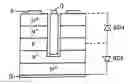
FIG. 3 illustrates a cross-sectional view of a N-Channel MOSFET of the present invention
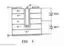
FIG. 4 illustrates a cross-sectional view of a P-Channel MOSFET of the present invention.
DETAILED DESCRIPTION OF THE PREFERRED EMBODIMENTS
FIG. 3 illustrates a cross-sectional view of a N-Channel MOSFET of the present invention, as shown, source S of the N-Channel MOSFET connected to N+ junction, N+ junction connected to N− junction, N− junction connected to P junction, the N+N−P junction as to form a fourth body diode BD4; Drain D of the N-Channel MOSFET connected to N+ junction, N+ junction connected to N− junction, N− junction connected to P junction, the N+N−P junction as to form a fifth body diode BD5; As shown, the P junction is common junction of the fourth body diode BD4 and fifth body diode BD5; According to a semiconductor theory that a breakdown voltage of a N-P junction is relate to the doping concentration and the depth of the N+ junction of source of N-Channel MOSFET and the N− junction drift region, and thus the N+ junction and the N− junction drift region of the present invention can be used increase the breakdown voltage; In the structures of the present invention, the doping concentration and the depth of the N+ junction and the N− junction drift region can be suitably varied according to a predetermined value of the breakdown voltage without limitation.
FIG. 4 illustrates a cross-sectional view of a P-Channel MOSFET of the present invention, as shown, source S of the P-Channel MOSFET connected to P+ junction, P+ junction connected to P− junction, P− junction connected to N junction, the P+P−N junction as to form a sixth body diode BD6; Drain D of the P-Channel MOSFET connected to P+ junction, P+ junction connected to P− junction, P− junction connected to N junction, the P+P−N junction as to form a seventh body diode BD7; As shown, the N junction is common junction of the sixth body diode BD6 and seventh body diode BD7; According to a semiconductor theory that a breakdown voltage of a P-N junction is relate to the doping concentration and the depth of the P+ junction of source of P-Channel MOSFET and the P− junction drift region, and thus the P+ junction and the P− junction drift region of the present invention can be used increase the breakdown voltage; In the structures of the present invention, the doping concentration and the depth of the P+ junction and the P− junction drift region can be suitably varied according to a predetermined value of the breakdown voltage without limitation.
While the invention has been described with respect to specific embodiments by way of illustration, many modification and changes will occur to those skilled in the art. It is therefore, to be understood that the append claims are intended to cover all such modifications and changes as fall within the true spirit and scope of the invention.
Claims
What is claimed is:1. A high source to drain breakdown voltage vertical field effect transistors having a body diode, said a body diode comprising:
a N+ junction, connected to source of N-Channel MOSFET;
a N− junction, connected to N+ junction; and
a P junction, connected to N− junction.
2. A high source to drain breakdown voltage vertical field effect transistors having a body diode, said a body diode comprising:
a P+ junction, connected to source of P-Channel MOSFET;
a P− junction, connected to P+ junction; and
a N junction, connected to P− junction.
Images & Drawings included:
Sources:
- United States Patent and Trademark Office - verify current appl. status at the USPTO↗
Recent applications in this class:
- » 20250072047 2025-02-27
Trench MOSFET and manufacturing method thereof - » 20250072046 2025-02-27
SEMICONDUCTOR DEVICE, METHOD OF MANUFACTURING SEMICONDUCTOR DEVICE, AND POWER CONVERSION DEVICE - » 20250072045 2025-02-27
LOW THRESHOLD HIGH DENSITY TRENCH MOSFET - » 20250072044 2025-02-27
POWER SEMICONDUCTOR DEVICES HAVING GATE TRENCHES WITH ASYMMETRICALLY ROUNDED UPPER AND LOWER TRENCH CORNERS AND/OR RECESSED GATE ELECTRODES AND METHODS OF FABRICATING SUCH DEVICES - » 20250056836 2025-02-13
SEMICONDUCTOR DEVICE AND METHOD OF MANUFACTURING SEMICONDUCTOR DEVICE - » 20250048674 2025-02-06
METHOD FOR PRODUCING A POWER FINFET, AND POWER FINFET - » 20250048673 2025-02-06
TRENCH MOSFET AND MANUFACTURING METHOD THEREOF - » 20250031409 2025-01-23
SEMICONDUCTOR COMPONENT AND METHOD FOR PRODUCING A SEMICONDUCTOR COMPONENT - » 20250031408 2025-01-23
POWER SEMICONDUCTOR DEVICE - » 20250022953 2025-01-16
SILICON CARBIDE SEMICONDUCTOR DEVICE AND METHOD OF MANUFACTURING SILICON CARBIDE SEMICONDUCTOR DEVICE