Article and method for manufacturing same
US20120021210A1
2012-01-26
12/968,424
2010-12-15
✅ Patent granted
US 8,431,239 B2
2013-04-30
-
-
Vera Katz
Altis Law Group, Inc.
2031-06-22
Abstract:
A article made by vacuum deposition, includes a substrate; and a color layer deposited on the substrate, wherein the color layer has an L* value between about 75 to about 80, a a* value between about −5 to about −10, and a b* value between about 15 to about 20 in the CIE LAB color space.
Inventors:
- Hsin-Pei CHANG 200 🇹🇼 Tu-Cheng, Taiwan
- WEN-RONG CHEN 195 🇹🇼 Tu-Cheng, Taiwan
- CHENG-SHI CHEN 213 🇹🇼 Tu-Cheng, Taiwan
- CHUANG MA 13 🇨🇳 Shenzhen, China
- HUAN-WU CHIANG 11 🇹🇼 Tu-Cheng, Taiwan
Assignee:
- HON HAI PRECISION INDUSTRY CO., LTD. 12,833 🇹🇼 Tu-Cheng, Taiwan
- HONG FU JIN PRECISION INDUSTRY (SHENZHEN) CO., LTD. 4,225 🇨🇳 Shenzhen City, China
- HON HAI PRECISION INDUSTRY CO., LTD. 10,014 🇹🇼 New Taipei, Taiwan
- HONG FU JIN PRECISION INDUSTRY (ShenZhen) CO., LTD. 2,585 🇨🇳 Shenzhen, China
Applicant:
Interested in similar patents?
Get notified when new applications in this technology area are published.
Classification:
C23C14/35 IPC
Coating by vacuum evaporation, by sputtering or by ion implantation of the coating forming material characterised by the process of coating; Sputtering by application of a magnetic field, e.g. magnetron sputtering
C23C14/0015 » CPC main
Coating by vacuum evaporation, by sputtering or by ion implantation of the coating forming material characterized by the colour of the layer
C23C14/022 » CPC further
Coating by vacuum evaporation, by sputtering or by ion implantation of the coating forming material; Pretreatment of the material to be coated; Cleaning or etching treatments by means of bombardment with energetic particles or radiation
C23C14/025 » CPC further
Coating by vacuum evaporation, by sputtering or by ion implantation of the coating forming material; Pretreatment of the material to be coated; Deposition of sublayers, e.g. to promote adhesion of the coating Metallic sublayers
C23C14/083 » CPC further
Coating by vacuum evaporation, by sputtering or by ion implantation of the coating forming material characterised by the coating material; Oxides of refractory metals or yttrium
C23C14/345 » CPC further
Coating by vacuum evaporation, by sputtering or by ion implantation of the coating forming material characterised by the process of coating; Sputtering; Applying energy to the substrate during sputtering using substrate bias
C23C14/3492 » CPC further
Coating by vacuum evaporation, by sputtering or by ion implantation of the coating forming material characterised by the process of coating; Sputtering Variation of parameters during sputtering
Y10T428/12611 » CPC further
Stock material or miscellaneous articles; All metal or with adjacent metals; Composite; i.e., plural, adjacent, spatially distinct metal components [e.g., layers, joint, etc.] with additional, spatially distinct nonmetal component Oxide-containing component
Y10T428/12826 » CPC further
Stock material or miscellaneous articles; All metal or with adjacent metals; Composite; i.e., plural, adjacent, spatially distinct metal components [e.g., layers, joint, etc.]; Transition metal-base component; Refractory [Group IVB, VB, or VIB] metal-base component Group VIB metal-base component
Y10T428/12847 » CPC further
Stock material or miscellaneous articles; All metal or with adjacent metals; Composite; i.e., plural, adjacent, spatially distinct metal components [e.g., layers, joint, etc.]; Transition metal-base component; Refractory [Group IVB, VB, or VIB] metal-base component; Group VIB metal-base component Cr-base component
Y10T428/26 » CPC further
Stock material or miscellaneous articles Web or sheet containing structurally defined element or component, the element or component having a specified physical dimension
Y10T428/265 » CPC further
Stock material or miscellaneous articles; Web or sheet containing structurally defined element or component, the element or component having a specified physical dimension; Coating layer not in excess of 5 mils thick or equivalent; Up to 3 mils 1 mil or less
B32B5/00 IPC
Layered products characterised by the non- homogeneity or physical structure, i.e. comprising a fibrous, filamentary, particulate or foam layer; Layered products characterised by having a layer differing constitutionally or physically in different parts
C01G37/02 IPC
Compounds of chromium Oxides or hydrates thereof
B32B9/00 IPC
Layered products characterised by particular substances used
B32B9/00 IPC
Layered products comprising a layer of a particular substance not covered by groups -
B32B15/00 IPC
Layered products comprising a layer of metal
B32B7/02 IPC
Layered products characterised by the relation between layers; Layered products characterised by the relative orientation of features between layers, or by the relative values of a measurable parameter between layers, i.e. products comprising layers having different physical, chemical or physicochemical properties; Layered products characterised by the interconnection of layers Physical, chemical or physicochemical properties
C23C14/06 IPC
Coating by vacuum evaporation, by sputtering or by ion implantation of the coating forming material characterised by the coating material
Description
BACKGROUND
1. Technical Field
The exemplary disclosure generally relates to articles and methods for manufacturing the articles.
2. Description of Related Art
Vacuum deposition is used to form a thin film or coating on housings of portable electronic devices, to improve the abrasion resistance. However, typical vacuum deposition only can deposit black or gold coatings on the housing so the housing has limited appearance compared to other processes used, such as anodic treatment.
Therefore, there is room for improvement within the art.
BRIEF DESCRIPTION OF THE DRAWINGS
Many aspects of the embodiments can be better understood with reference to the following drawings. The components in the drawings are not necessarily drawn to scale, the emphasis instead being placed upon clearly illustrating the principles of the exemplary embodiment of an article and method for manufacturing the article. Moreover, in the drawings like reference numerals designate corresponding parts throughout the several views. Wherever possible, the same reference numbers are used throughout the drawings to refer to the same or like elements of an embodiment.
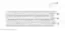
FIG. 1 illustrates a cross-sectional view of an exemplary embodiment of an article.
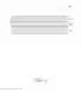
FIG. 2 is a schematic view of a magnetron sputtering coating machine for manufacturing the article in FIG. 1.
DETAILED DESCRIPTION
Referring to FIG. 1, an exemplary embodiment of an article 10 manufactured, by coating process, such as by vacuum deposition, includes a substrate 11, a bonding layer 13 deposited on the substrate 11 and a color layer 15 deposited on the bonding layer 13 opposite to the substrate 11. The article 10 may be a housing of electronic device. The substrate 11 is made of metal, glass, plastic or ceramic.
The bonding layer 13 is formed between the substrate 11 and the color layer 15 for improving the binding force between the substrate 11 and the color layer 15. The bonding layer 13 may be comprised of chromium. The bonding layer 13 has a thickness ranging from about 0.01 micrometer to about 0.1 micrometer, and in this embodiment has a thickness of 0.05 micrometer. The bonding layer 13 in this embodiment has a color that does not affect the color of the color layer 15, such as silver, white, or gray.
The color layer 15 is a chromium oxide layer. In this exemplary embodiment, the color layer 15 may be made of Chromium (II) oxide (CrO). The color layer 15 is green which has an L* value between about 75 to about 80, a a* value between about −5 to about −10, and a b* value between about 15 to about 20 in the CIE L*a*b* (CIE LAB) color space, so the color layer 15 is substantially green (my dear steve, this is ok?). The color layer 15 has a thickness ranging from about 0.5 micrometer to about 3 micrometer. In this embodiment, it has a thickness of about 2 micrometer.
A method for manufacturing the article 10 manufactured by vacuum deposition may include at least the following steps.
A substrate 11 is provided. The substrate 11 may be made of metal, glass, plastic or ceramic.
The substrate 11 is pretreated. For example, the substrate 11 may be washed with a solution (e.g., alcohol or Acetone) in an ultrasonic cleaner, to remove, e.g., grease, dirt, and/or impurities. The substrate 11 is then dried. The substrate 11 may also be cleaned by an argon plasma cleaning. The substrate 11 is retained on a rotating bracket 50 in a vacuum chamber 60 of a magnetron sputtering coating machine 100. The vacuum level of the vacuum chamber 60 is adjusted to 8.0×10⁻³ Pa. Pure argon is floated into the vacuum chamber 60 at a flux of about 300 sccm (Standard Cubic Centimeters per Minute) to 600 sccm; a bias voltage applied to the substrate 11 in a range from −300 to −800 volts for a time of about 5 to about 15 min. So the substrate 11 is washed by argon plasma, to further remove the grease or dirt. Thus, a binding force between the substrate 11 and the color layer 15 is enhanced.
The bonding layer 13 is deposited on the substrate 11 by magnetron sputtering. The temperature in the vacuum chamber 60 is adjusted to 120˜180° C., i.e., the reaction temperature is about 120- about 180° C.; the argon is floated into the vacuum chamber 60 at a flux from about 100 sccm to about 500 sccm, i.e. The reaction gas of depositing the bonding layer 13 is argon. The speed of the rotating bracket 50 is adjusted to 2 to 3 rpm (revolution per minute). A chromium target 70 is evaporated and a bias voltage applied to the substrate 11 in a range from about −100 to about −500 volts for a time of about 5 min to about 15 min, to deposit the bonding layer 13 on the substrate 11.
The color layer 15 is deposited on the bonding layer 13 by magnetron sputtering. The temperature in the vacuum chamber 60 is kept from about 120° C. to about 180° C., i.e., the reaction temperature is about 120- about 180° C.; the argon is continuously floated into the vacuum chamber 60 at a flux from about 100 sccm to about 500 sccm and oxygen is floated into the vacuum at a flux from 5 sccm to 100 sccm, i.e, the reaction gas of depositing the color layer 15 is argon and oxygen; the speed of the rotating bracket 50 is kept from about 2 to about 3 revolution per minute (rpm); the chromium target 70 is continuously evaporated; a bias voltage applied to the substrate 11 is in a range from about −100 to about −300 volts for a time of about 20 min to about 60 min, to deposit the color layer 15 on the bonding layer.
The color layer 15 is green which has an L* value between 75 to 80, a a* value between about −5 to about −10, and a b* value between about 15 to about 20 in the CIE L*a*b* (CIE LAB) color space, and the color layer 15 is substantially green.
It is to be understood, however, that even through numerous characteristics and advantages of the exemplary disclosure have been set forth in the foregoing description, together with details of the system and function of the disclosure, the disclosure is illustrative only, and changes may be made in detail, especially in matters of shape, size, and arrangement of parts within the principles of the disclosure to the full extent indicated by the broad general meaning of the terms in which the appended claims are expressed.
Claims
What is claimed is:1. An article, comprising:
a substrate; and
a color layer deposited on the substrate, wherein the color layer has a L* value between 75 to 80, an a* value between −5 to −10, and a b* value between 15 to 20 in the CIE LAB color space, and the color layer is substantially green.
2. The article as claimed in claim 1, wherein the color layer is a chromium oxide layer.
3. The article as claimed in claim 2, wherein the color layer is made of Chromium(II) oxide.
4. The article as claimed in claim 1, wherein the color layer has a thickness ranging from about 0.5 micrometer to about 3 micrometer.
5. The article as claimed in claim 1, further comprising a bonding layer formed between the substrate and the color layer for improving the binding force between the substrate and the color layer.
6. The article as claimed in claim 5, wherein the bonding layer is comprised of chromium.
7. The article as claimed in claim 5, wherein the bonding layer has a thickness ranging from about 0.01 micrometer to about 0.1 micrometer.
8. The article as claimed in claim 1, wherein the substrate is made of metal, glass, plastic or ceramic.
9. A method for manufacturing a article comprising steps of:
providing a substrate; and
depositing a color layer on the substrate by magnetron sputtering, wherein the substrate is retained in a vacuum chamber, the temperature in the vacuum chamber is from 120° C. to 180° C.; argon is floated into the vacuum chamber at a flux from about 100 sccm to about 500 sccm and oxygen is floated into the vacuum at a flux from 5 sccm to 100 sccm; a chromium target is evaporated; a bias voltage applied to the substrate is in a range from −100 to −300 volts for a time of about 20 min to about 60 min, to deposit the color layer on the substrate.
10. The method of claim 9, wherein the color layer has a L* value between 75 to 80, an a* value between −5 to −10, and a b* value between 15 to 20 in the CIE LAB color space, and the color layer is substantially green.
11. The method of claim 9, wherein the color layer is a chromium oxide layer.
12. The method of claim 9, further including a step of depositing a bonding layer on the substrate by magnetron sputtering between depositing a color layer on the substrate, wherein during the step of depositing the bonding layer, the temperature in the vacuum chamber 60 is adjusted to 120˜180° C.; the argon is floated into the vacuum chamber 60 at a flux from about 100 sccm to about 500 sccm; the chromium target is evaporated; a bias voltage applied to the substrate is in a range from −100 to −500 volts for a time of about 5 min to about 15 min, to deposit the bonding layer on the substrate.
Images & Drawings included:

Sources:
- United States Patent and Trademark Office - verify current appl. status at the USPTO↗
Similar patent applications:
- » 20250093771
MOLD, MANUFACTURING METHOD, FILM FORMING METHOD, ARTICLE MANUFACTURING METHOD, AND IMPRINT APPARATUS - » 20220244700
Information processing apparatus, information processing method, article manufacturing system, and article manufacturing method - » 20170062230
Etching method, article manufacturing method, and etching apparatus - » 20200198127
Robot apparatus, control method of robot apparatus, power transmission module, power reception module, power supply method, article manufacturing method using robot apparatus, and storage medium - » 20120126459
Drawing apparatus, method of manufacturing article, method of manufacturing deflecting apparatus, and method of manufacturing drawing apparatus - » 20120188536
Imprint apparatus, detection method, article manufacturing method, and foreign particle detection apparatus - » 20200273203
CALCULATION METHOD, ARTICLE MANUFACTURING METHOD, RECORDING MEDIUM, INFORMATION PROCESSING APPARATUS, AND SYSTEM - » 20190392607
IMAGE PROCESSING APPARATUS, SYSTEM, IMAGE PROCESSING METHOD, ARTICLE MANUFACTURING METHOD, AND NON-TRANSITORY COMPUTER-READABLE STORAGE MEDIUM - » 20190061207
Imprint apparatus, imprint method, article manufacturing method, molding apparatus, and molding method - » 20220187702
Imprint apparatus, imprint method, article manufacturing method, and storage medium
Recent applications in this class:
- » 20250154638 2025-05-15
PROCESS FOR DECORATING WATCH COMPONENTS - » 20250146118 2025-05-08
METHODS TO IMPART COLOR AND DURABLE PROPERTIES TO SUBSTRATES - » 20230077782 2023-03-16
APPROACHES TO MODIFYING A COLOR OF AN ELECTROCHROMIC STACK IN A TINTED STATE - » 20220389560 2022-12-08
Method for producing a coating - » 20220235448 2022-07-28
METHOD FOR VACUUM COATING A COLORFUL FILM - » 20210222279 2021-07-22
Method for regulating color of hard coating, hard coating, and method for preparing the same - » 20200048756 2020-02-13
Reflector for vehicle lighting - » 20190352763 2019-11-21
Method for implanting single or multiply charged ions into a surface of a treated object and device for implementation of the method - » 20190323115 2019-10-24
Color film and method of forming the same - » 20190194794 2019-06-27
CERAMIC COLORING METHOD AND A CERAMIC PIECE FOR ELECTRONIC PRODUCTS
Recent applications for this Assignee:
- » 20250218287 2025-07-03
METHOD OF GENERATING AND PROMPTING TRAFFIC INFORMATION, AND ROADSIDE DEVICE THEREOF - » 20250178535 2025-06-05
METHOD FOR CONSTRUCTING 3D PANORAMIC VIEW MODEL, VEHICLE-MOUNTED DEVICE, AND STORAGE MEDIUM - » 20250074444 2025-03-06
METHOD FOR EARLY WARNING A BLIND AREA, ELECTRONIC DEVICE AND STORAGE MEDIUM - » 20240416754 2024-12-19
DISPLAY CONTROL DEVICE, DISPLAY EQUIPMENT, AND VEHICLE EMPLOYING DEVICE - » 20240411051 2024-12-12
Light-emitting device array and optical transceiver system having the same - » 20240324114 2024-09-26
DISPLAY CONTROL DEVICE AND VEHICLE EMPLOYING DEVICE - » 20240295957 2024-09-05
METHOD FOR CONTROLLING ELECTRONIC DEVICE, ELECTRONIC DEVICE AND COMPUTER STROAGE MEDIUM EMPLOYING METHOD - » 20240257357 2024-08-01
METHOD FOR DETECTING OBSTACLES, ELECTRONIC DEVICE, AND STORAGE MEDIUM - » 20240203133 2024-06-20
LANE LINE RECOGNITION METHOD, ELECTRONIC DEVICE AND STORAGE MEDIUM - » 20240194999 2024-06-13
Robot using limiting device for locking battery