LDMOS structure
US20120037984A1
2012-02-16
13/207,426
2011-08-11
✅ Patent granted
US 8,502,268 B2
2013-08-06
-
-
Tan N Tran | Scott R Wilson
2031-10-05
Abstract:
A LDMOS structure includes a gate, a source, a drain and a bulk. The gate includes a polycrystalline silicon layer, the source includes a P-implanted layer, the drain includes the P-implanted layer, a P-well layer, and a deep P-well layer. A bulk terminal is connected through the P-implanted layer, the P-well layer, the deep P-well layer, and a P-type buried layer to the bulk. The LDMOS structure is able to be produced without any extra masking step, and it has compact structure, low on-resistance, and is able to withstand high current and high voltage.
Assignee:
- IPGoal Microelectronics (SiChuan) Co., Ltd. 38 🇨🇳 Chengdu, Sichuan Province, China
Applicant:
Interested in similar patents?
Get notified when new applications in this technology area are published.
Classification:
H01L29/66 IPC
Semiconductor devices adapted for rectifying, amplifying, oscillating or switching, or capacitors or resistors with at least one potential-jump barrier or surface barrier, e.g. PN junction depletion layer or carrier concentration layer; Details of semiconductor bodies or of electrodes thereof; Multistep manufacturing processes therefor Types of semiconductor device ; Multistep manufacturing processes therefor
H01L29/0847 » CPC further
Semiconductor devices adapted for rectifying, amplifying, oscillating or switching, or capacitors or resistors with at least one potential-jump barrier or surface barrier, e.g. PN junction depletion layer or carrier concentration layer; Details of semiconductor bodies or of electrodes thereof; Multistep manufacturing processes therefor; Semiconductor bodies ; Multistep manufacturing processes therefor characterised by their shape; characterised by the shapes, relative sizes, or dispositions of the semiconductor regions ; characterised by the concentration or distribution of impurities within semiconductor regions with semiconductor regions connected to an electrode carrying current to be rectified, amplified or switched and such electrode being part of a semiconductor device which comprises three or more electrodes; Source or drain regions of field-effect devices of field-effect transistors with insulated gate
H01L29/0692 » CPC further
Semiconductor devices adapted for rectifying, amplifying, oscillating or switching, or capacitors or resistors with at least one potential-jump barrier or surface barrier, e.g. PN junction depletion layer or carrier concentration layer; Details of semiconductor bodies or of electrodes thereof; Multistep manufacturing processes therefor; Semiconductor bodies ; Multistep manufacturing processes therefor characterised by their shape; characterised by the shapes, relative sizes, or dispositions of the semiconductor regions ; characterised by the concentration or distribution of impurities within semiconductor regions characterised by the shape, relative sizes or dispositions of the semiconductor regions or junctions between the regions Surface layout
H01L29/78 IPC
Semiconductor devices adapted for rectifying, amplifying, oscillating or switching, or capacitors or resistors with at least one potential-jump barrier or surface barrier, e.g. PN junction depletion layer or carrier concentration layer; Details of semiconductor bodies or of electrodes thereof; Multistep manufacturing processes therefor; Types of semiconductor device ; Multistep manufacturing processes therefor controllable by only the electric current supplied, or only the electric potential applied, to an electrode which does not carry the current to be rectified, amplified or switched; Unipolar devices, e.g. field effect transistors; Field effect transistors with field effect produced by an insulated gate
Description
BACKGROUND OF THE PRESENT INVENTION
1. Field of Invention
The present invention relates to semiconductors, and more particularly to a LDMOS structure which has compact structure, low on-resistance, and is able to withstand high current and high voltage.
2. Description of Related Arts
With the continuous development of the power semiconductor technology and system integration technology, research on power devices has drawn more and more attentions. Because power devices play a crucial role in the size, weight, price, efficiency, performance and reliability of the power semiconductor, new technologies have been applied to the Laterally Diffused Metal Oxide Semiconductor (LDMOS) device to meet market requirements. It is for this reason, the LDMOS structures and its production processes have improved continuously, and various derivative structures of LDMOS are emerging in an endless stream. Therefore, according to requirements in practical applications, it is necessary to provide a kind of LDMOS structure which has compact structure, low on-resistance, and can withstand high current and high voltage.
SUMMARY OF THE PRESENT INVENTION
An object of the present invention is to provide a LDMOS structure which has compact structure, low on-resistance, and is able to withstand high current and high voltage.
Accordingly, in order to accomplish the above objects, the present invention provides a LDMOS structure, which comprises a gate, a source, a drain and a bulk, wherein the gate comprises a polycrystalline silicon layer, the source comprises a P-implanted layer, the drain comprises the P-implanted layer, a P-well layer, and a deep P-well layer, wherein a bulk terminal is connected through the P-implanted layer, the P-well layer, the deep P-well layer, and a P-type buried layer to the bulk.
Preferably, the drain has a plurality of drain regions, the source has a plurality of source regions, the gate has a plurality of gate regions, wherein each source region is surrounded by four drain regions, each drain region is surrounded by four source regions, and each gate region is located between a source region and a drain region.
Preferably, the LDMOS structure further comprises a back gate, wherein the back gate comprises a N-implanted layer, a N-well layer, a deep N-well layer, a N-epitaxial layer, and a N-type buried layer, and has a plurality of back gate regions, wherein each source region is located near a back gate region.
Preferably, the LDMOS structure further comprises a field-oxide layer.
Preferably, the bulk is a P-type bulk, the bulk terminal is a P-type bulk terminal.
Preferably, the LDMOS is a P-channel LDMOS.
Without any extra masking step, the LDMOS structure of the present invention is able to be produced just by using prior art methods. Furthermore, it has compact structure, low on-resistance, and is able to withstand high current and high voltage.
BRIEF DESCRIPTION OF THE DRAWINGS
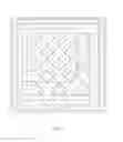
FIG. 1 is a plane diagram of a LDMOS structure according to a preferred embodiment of the present invention.
FIG. 2 is a sectional diagram of the LDMOS structure according to above preferred embodiment of the present invention.
DETAILED DESCRIPTION OF THE PREFERRED EMBODIMENT
Referring to FIG. 1 of the drawings, a plane diagram of a Laterally Diffused Metal Oxide Semiconductor (LDMOS) structure according to a preferred embodiment of the present invention is illustrated, in which the LDMOS structure comprises a drain D, a source S, a gate G, a back gate B, and a P-type bulk PSUB. As shown in FIG. 1, the drain D has a plurality of drain regions; the source B has a plurality of source regions; the gate G has a plurality of gate regions; the back gate B has a plurality of back gate regions, wherein each source region is surrounded by four drain regions, each drain region is surrounded by four source regions, each gate region is located between a source region and a drain region, and each source region is located near a back gate region.
Also, referring to FIG. 2, which shows a sectional diagram cut along a 45-degree diagonal of the FIG. 1, namely, along the direction shown by arrows. As shown in FIG. 2, the LDMOS structure comprises a field-oxide layer FOX, a P-implanted layer P+, a P-well layer LVPW, a deep P-well layer HVPW, a N-epitaxial layer NEPI, a N-implanted layer N+, a N-well layer LVNW, a deep N-well layer HVNW, a P-type buried layer PBL, a N-type buried layer NBL, a polycrystalline silicon layer POLY, the P-type bulk PSUB, the drain D, the source S, the gate G, the back gate B and a P-type bulk terminal SUB.
Here, the back gate B comprises the N-implanted layer N+, the N-well layer LVNW, the deep N-well layer HVNW, the N-epitaxial layer NEPI, and the N-type buried layer NBL, wherein the N-implanted layer N+ is next to the P-implanted layer P+, and the N-implanted layer N+ and the P-implanted layer P+ are both located within the N-well layer LVNW; the N-well layer LVNW is semi-enclosed by the deep N-well layer HVNW; the N-well layer LVNW and the deep N-well layer HVNW are both located within the N-epitaxial layer NEPI; the N-epitaxial layer NEPI is located on the N-type buried layer NBL; and the N-type buried layer NBL is located on the P-type bulk PSUB.
The source S comprises the P-implanted layer P+, wherein the P-implanted layer P+ is located within the N-well layer LVNW and next to the N-implanted layer N+.
The gate G comprises the polycrystalline silicon layer POLY, wherein the polycrystalline silicon layer POLY is located on the N-well layer LVNW.
The drain D comprises the P-implanted layer P+, the P-well layer LVPW, and the deep P-well layer HVPW, wherein the P-implanted layer P+ is located within the P-well layer LVPW, and the P-well layer LVPW is located within the deep P-well layer HVPW.
The P-type bulk terminal SUB is connected through the P-implanted layer P+, the P-well layer LVPW, the deep P-well layer HVPW, and the P-type buried layer PBL to the P-type bulk PSUN.
The field-oxide layer FOX is located below the polycrystalline silicon layer POLY.
The LDMOS structure of the present invention is designed based on N-epitaxial BiCMOS technology, in which a low-doped drift region is introduced between the channel and the drain region. When a high voltage is applied to the drain D, due to a lower concentration of the drift region, most of voltage is applied to the drift region, so that the LDMOS structure is able to withstand higher voltage. The LDMOS structure of the present invention provides the best epitaxial layer quality and the best length of the drift region, so it can get a minimum on-resistance with a certain source-drain breakdown voltage. Furthermore, the LDMOS structure is able to arrange the drain-source units in an array very closely, so as to obtain a smaller on-resistance. The FIG. 1 shows a net structure, in which there are four drain regions formed around a source region, and there are four source regions formed around a drain region. This structure is not prone to local avalanche breakdown. Also, the diagonal placement of the source region and the drain region can enhance the current limiting ability of the source and the drain, so as to improve the stabilities of above elements under extreme condition. Therefore, the combination of these advantages as described above makes the LDMOS structure is often employed on transient overload conditions.
The LDMOS structure of the present invention a novel structure based on BiCMOS technology, and it can be produced according to prior art methods without any extra masking step. Furthermore, it has compact structure, low on-resistance, and can withstand high current and high voltage.
One skilled in the art will understand that the embodiment of the present invention as shown in the drawings and described above is exemplary only and not intended to be limiting.
It will thus be seen that the objects of the present invention have been fully and effectively accomplished. Its embodiments have been shown and described for the purposes of illustrating the functional and structural principles of the present invention and is subject to change without departure from such principles. Therefore, this invention includes all modifications encompassed within the spirit and scope of the following claims.
Claims
What is claimed is:1. A Laterally Diffused Metal Oxide Semiconductor (LDMOS) structure, comprising a gate, a source, a drain and a bulk, wherein the gate comprises a polycrystalline silicon layer, the source comprises a P-implanted layer, and the drain comprises the P-implanted layer, a P-well layer, and a deep P-well layer, wherein the P-implanted layer is located within the P-well layer, and the P-well layer is located within the deep P-well layer, wherein a bulk terminal is connected through the P-implanted layer, the P-well layer, the deep P-well layer, and a P-type buried layer to the bulk.
2. The LDMOS structure, as recited in claim 1, wherein the drain has a plurality of drain regions, the source has a plurality of source regions, the gate has a plurality of gate regions, wherein each source region is surrounded by four drain regions, each drain region is surrounded by four source regions, and each gate region is located between a source region and a drain region.
3. The LDMOS structure, as recited in claim 1, further comprising a back gate having a plurality of back gate regions, and comprising a N-implanted layer, a N-well layer, a deep N-well layer, a N-epitaxial layer, and a N-type buried layer, wherein the N-implanted layer is next to the P-implanted layer, the N-implanted layer and the P-implanted layer are both located within the N-well layer, the N-well layer is semi-enclosed by the deep N-well layer, the N-well layer and the deep N-well layer are both located within the N-epitaxial layer, the N-epitaxial layer is located on the N-type buried layer, and the N-type buried layer is located on the bulk, wherein each source region is located near a back gate region.
4. The LDMOS structure, as recited in claim 2, further comprising a back gate having a plurality of back gate regions, and comprising a N-implanted layer, a N-well layer, a deep N-well layer, a N-epitaxial layer, and a N-type buried layer, wherein the N-implanted layer is next to the P-implanted layer, the N-implanted layer and the P-implanted layer are both located within the N-well layer, the N-well layer is semi-enclosed by the deep N-well layer, the N-well layer and the deep N-well layer are both located within the N-epitaxial layer, the N-epitaxial layer is located on the N-type buried layer, and the N-type buried layer is located on the bulk, wherein each source region is located near a back gate region.
5. The LDMOS structure, as recited in claim 3, further comprising a field-oxide layer located below the polycrystalline silicon layer.
6. The LDMOS structure, as recited in claim 4, further comprising a field-oxide layer located below the polycrystalline silicon layer.
7. The LDMOS structure, as recited in claim 1, wherein the bulk is a P-type bulk, the bulk terminal is a P-type bulk terminal
8. The LDMOS structure, as recited in claim 2, wherein the bulk is a P-type bulk, the bulk terminal is a P-type bulk terminal
9. The LDMOS structure, as recited in claim 3, wherein the bulk is a P-type bulk, the bulk terminal is a P-type bulk terminal
10. The LDMOS structure, as recited in claim 4, wherein the bulk is a P-type bulk, the bulk terminal is a P-type bulk terminal
11. The LDMOS structure, as recited in claim 5, wherein the bulk is a P-type bulk, the bulk terminal is a P-type bulk terminal
12. The LDMOS structure, as recited in claim 6, wherein the bulk is a P-type bulk, the bulk terminal is a P-type bulk terminal
13. The LDMOS structure, as recited in claim 1, wherein the LDMOS is a P-channel LDMOS.
14. The LDMOS structure, as recited in claim 2, wherein the LDMOS is a P-channel LDMOS.
15. The LDMOS structure, as recited in claim 4, wherein the LDMOS is a P-channel LDMOS.
16. The LDMOS structure, as recited in claim 6, wherein the LDMOS is a P-channel LDMOS.
17. The LDMOS structure, as recited in claim 7, wherein the LDMOS is a P-channel LDMOS.
18. The LDMOS structure, as recited in claim 10, wherein the LDMOS is a P-channel LDMOS.
19. The LDMOS structure, as recited in claim 11, wherein the LDMOS is a P-channel LDMOS.
20. The LDMOS structure, as recited in claim 12, wherein the LDMOS is a P-channel LDMOS.
Images & Drawings included:


Sources:
- United States Patent and Trademark Office - verify current appl. status at the USPTO↗
Similar patent applications:
- » 15181780
Integrated circuits including LDMOS transistor structures and methods for fabricating LDMOS transistor structures - » 20180053842
LDMOS transistor structures and integrated circuits including LDMOS transistor structures - » 20240379823
BEVEL STRUCTURE AND ITS MANUFACTURING METHOD, LDMOS STRUCTURE AND ITS MANUFACTURING METHOD - » 20150145034
LDMOS STRUCTURE AND MANUFACTURING METHOD THEREOF - » 10951259
Trench-gate LDMOS structures - » 20090273026
Trench-gate LDMOS structures - » 20120248528
TRENCH-GATE LDMOS STRUCTURES - » 20120058608
Method of fabricating SOI super-junction LDMOS structure capable of completely eliminating substrate-assisted depletion effects - » 20060220179
Method for forming an improved isolation junction in high voltage LDMOS structures - » 20130082325
One-time programmable device having an LDMOS structure
Recent applications in this class:
- » 20240395868 2024-11-28
SEMICONDUCTOR DEVICE WITH ENHANCED DRAIN - » 20240355884 2024-10-24
PURIFIED SURFACE REGION OF AN OXIDE SEMICONDUCTOR, AND METHOD OF NEAR-SURFACE PURIFICATION - » 20230215918 2023-07-06
LDMOS TRANSISTOR AND METHOD OF FORMING THE LDMOS TRANSISTOR WITH IMPROVED RDS*CGD - » 20230207630 2023-06-29
SEMICONDUCTOR DEVICE - » 20230138658 2023-05-04
SEMICONDUCTOR DEVICE - » 20230114260 2023-04-13
SEMICONDUCTOR DEVICE AND METHOD OF MANUFACTURING SEMICONDUCTOR DEVICE - » 20220190114 2022-06-16
Vertical MOSFET having trench gate structure containing silicon carbide - » 20210257455 2021-08-19
Silicon carbide semiconductor device - » 20200328275 2020-10-15
Semiconductor devices with a sloped surface - » 20200219977 2020-07-09
High voltage demos transistor with improved threshold voltage matching
Recent applications for this Assignee:
- » 20150030114 2015-01-29
Frequency locking system - » 20150002193 2015-01-01
Driver having low power consumption and method thereof - » 20140176354 2014-06-26
Sampling circuit for ADC - » 20140176241 2014-06-26
High-frequency bandwidth amplifying circuit - » 20140143584 2014-05-22
Circuit for generating peripheral clock for USB and method therefor - » 20140133532 2014-05-15
Serial data transmission system and method - » 20140126747 2014-05-08
Power amplifying circuit and system - » 20140126673 2014-05-08
Differential signal detecting device - » 20140089372 2014-03-27
Divider logic circuit and implement method therefor - » 20140086432 2014-03-27
POP noise suppression circuit and system