Coated article
US20120094095A1
2012-04-19
13/189,986
2011-07-25
✅ Patent granted
US 8,361,635 B2
2013-01-29
-
-
Michael La Villa
Altis Law Group, Inc.
2031-07-25
Abstract:
A coated article is described. The coated article includes a substrate, a combining layer formed on the substrate, a plurality of chromium nitride layers and a plurality of copper-zinc alloy layers formed on the combining layer. The combining layer is a chromium layer. Each chromium nitride layer interleaves with one copper-zinc alloy layer. A method for making the coated article is also described.
Inventors:
- Hsin-Pei CHANG 200 🇹🇼 Tu-Cheng, Taiwan
- WEN-RONG CHEN 195 🇹🇼 Tu-Cheng, Taiwan
- CHENG-SHI CHEN 213 🇹🇼 Tu-Cheng, Taiwan
- CONG LI 40 🇨🇳 Shenzhen City, China
- HUANN-WU CHIANG 185 🇹🇼 Tu-Cheng, Taiwan
- HSIN-PEI CHANG 86 🇹🇼 New Taipei, Taiwan
- CHENG-SHI CHEN 92 🇹🇼 New Taipei, Taiwan
- WEN-RONG CHEN 86 🇹🇼 New Taipei, Taiwan
- HUANN-WU CHIANG 89 🇹🇼 New Taipei, Taiwan
- Cong Li 37 🇨🇳 Shenzhen, China
Assignee:
- HON HAI PRECISION INDUSTRY CO., LTD. 12,833 🇹🇼 Tu-Cheng, Taiwan
- HONG FU JIN PRECISION INDUSTRY (SHENZHEN) CO., LTD. 4,225 🇨🇳 Shenzhen City, China
- HON HAI PRECISION INDUSTRY CO., LTD. 10,014 🇹🇼 New Taipei, Taiwan
- HONG FU JIN PRECISION INDUSTRY (ShenZhen) CO., LTD. 2,585 🇨🇳 Shenzhen, China
Applicant:
Interested in similar patents?
Get notified when new applications in this technology area are published.
Classification:
B32B15/04 IPC
Layered products comprising a layer of metal comprising metal as the main or only constituent of a layer, next to another layer of a
C23C14/025 » CPC main
Coating by vacuum evaporation, by sputtering or by ion implantation of the coating forming material; Pretreatment of the material to be coated; Deposition of sublayers, e.g. to promote adhesion of the coating Metallic sublayers
C23C14/0641 » CPC further
Coating by vacuum evaporation, by sputtering or by ion implantation of the coating forming material characterised by the coating material Nitrides
C23C14/185 » CPC further
Coating by vacuum evaporation, by sputtering or by ion implantation of the coating forming material characterised by the coating material; Metallic material, boron or silicon on other inorganic substrates by cathodic sputtering
C23C14/34 » CPC further
Coating by vacuum evaporation, by sputtering or by ion implantation of the coating forming material characterised by the process of coating Sputtering
C23C28/32 » CPC further
Coating for obtaining at least two superposed coatings either by methods not provided for in a single one of groups - or by combinations of methods provided for in subclasses and or; Coatings combining at least one metallic layer and at least one inorganic non-metallic layer including at least one pure metallic layer
C23C28/321 » CPC further
Coating for obtaining at least two superposed coatings either by methods not provided for in a single one of groups - or by combinations of methods provided for in subclasses and or; Coatings combining at least one metallic layer and at least one inorganic non-metallic layer including at least one pure metallic layer with at least one metal alloy layer
C23C28/34 » CPC further
Coating for obtaining at least two superposed coatings either by methods not provided for in a single one of groups - or by combinations of methods provided for in subclasses and or; Coatings combining at least one metallic layer and at least one inorganic non-metallic layer including at least one inorganic non-metallic material layer, e.g. metal carbide, nitride, boride, silicide layer and their mixtures, enamels, phosphates and sulphates
Y10T428/12479 » CPC further
Stock material or miscellaneous articles; All metal or with adjacent metals Porous [e.g., foamed, spongy, cracked, etc.]
Y10T428/12576 » CPC further
Stock material or miscellaneous articles; All metal or with adjacent metals; Composite; i.e., plural, adjacent, spatially distinct metal components [e.g., layers, joint, etc.] with additional, spatially distinct nonmetal component Boride, carbide or nitride component
Y10T428/12632 » CPC further
Stock material or miscellaneous articles; All metal or with adjacent metals; Composite; i.e., plural, adjacent, spatially distinct metal components [e.g., layers, joint, etc.] Four or more distinct components with alternate recurrence of each type component
Y10T428/12792 » CPC further
Stock material or miscellaneous articles; All metal or with adjacent metals; Composite; i.e., plural, adjacent, spatially distinct metal components [e.g., layers, joint, etc.]; Transition metal-base component; Group IIB metal-base component Zn-base component
Y10T428/12847 » CPC further
Stock material or miscellaneous articles; All metal or with adjacent metals; Composite; i.e., plural, adjacent, spatially distinct metal components [e.g., layers, joint, etc.]; Transition metal-base component; Refractory [Group IVB, VB, or VIB] metal-base component; Group VIB metal-base component Cr-base component
Y10T428/12903 » CPC further
Stock material or miscellaneous articles; All metal or with adjacent metals; Composite; i.e., plural, adjacent, spatially distinct metal components [e.g., layers, joint, etc.]; Transition metal-base component; Group VIII or IB metal-base component Cu-base component
Y10T428/2495 » CPC further
Stock material or miscellaneous articles; Structurally defined web or sheet [e.g., overall dimension, etc.] including components having same physical characteristic in differing degree Thickness [relative or absolute]
Y10T428/24967 » CPC further
Stock material or miscellaneous articles; Structurally defined web or sheet [e.g., overall dimension, etc.] including components having same physical characteristic in differing degree; Thickness [relative or absolute] Absolute thicknesses specified
Y10T428/249957 » CPC further
Stock material or miscellaneous articles; Web or sheet containing structurally defined element or component; Composite having voids in a component [e.g., porous, cellular, etc.]; Void-containing component partially impregnated with adjacent component; Void-containing component is inorganic Inorganic impregnant
Y10T428/24997 » CPC further
Stock material or miscellaneous articles; Web or sheet containing structurally defined element or component; Composite having voids in a component [e.g., porous, cellular, etc.]; Inorganic matrix in void-containing component Of metal-containing material
Y10T428/265 » CPC further
Stock material or miscellaneous articles; Web or sheet containing structurally defined element or component, the element or component having a specified physical dimension; Coating layer not in excess of 5 mils thick or equivalent; Up to 3 mils 1 mil or less
Y10T428/31678 » CPC further
Stock material or miscellaneous articles; Composite [nonstructural laminate] Of metal
C23C14/14 IPC
Coating by vacuum evaporation, by sputtering or by ion implantation of the coating forming material characterised by the coating material Metallic material, boron or silicon
C23C14/35 IPC
Coating by vacuum evaporation, by sputtering or by ion implantation of the coating forming material characterised by the process of coating; Sputtering by application of a magnetic field, e.g. magnetron sputtering
B32B7/02 IPC
Layered products characterised by the relation between layers; Layered products characterised by the relative orientation of features between layers, or by the relative values of a measurable parameter between layers, i.e. products comprising layers having different physical, chemical or physicochemical properties; Layered products characterised by the interconnection of layers Physical, chemical or physicochemical properties
B32B15/01 IPC
Layered products comprising a layer of metal all layers being exclusively metallic
B32B18/00 IPC
Layered products essentially comprising ceramics, e.g. refractory products
B32B15/20 IPC
Layered products comprising a layer of metal comprising aluminium or copper
Description
CROSS-REFERENCE TO RELATED APPLICATIONS
This application is one of the four related co-pending U.S. patent applications listed below. All listed applications have the same assignee. The disclosure of each of the listed applications is incorporated by reference into the other listed applications.
| Attorney | ||
| Docket | ||
| No. | Title | Inventors |
| US 35705 | COATED ARTICLE AND METHOD | HSIN-PEI CHANG |
| FOR MAKING THE SAME | et al. | |
| US 35707 | COATED ARTICLE AND METHOD | HSIN-PEI CHANG |
| FOR MAKING THE SAME | et al. | |
| US 35708 | COATED ARTICLE AND METHOD | HSIN-PEI CHANG |
| FOR MAKING THE SAME | et al. | |
| US 35709 | COATED ARTICLE AND METHOD | HSIN-PEI CHANG |
| FOR MAKING THE SAME | et al. | |
BACKGROUND
1. Technical Field
The present disclosure relates to coated articles, particularly to a coated article having an antibacterial effect and a method for making the coated article.
2. Description of Related Art
To make the living environment more hygienic and healthy, a variety of antibacterial products have been produced by coating antibacterial metal films on the substrate of the products. The metal may be copper (Cu), zinc (Zn), or silver (Ag). However, the coated metal films are soft and poorly bond to the substrate, so the metal films are prone to abrasion. Moreover, the metal ions within the metal films rapidly dissolve from killing bacterium, so the metal films always have a short useful lifespan.
Therefore, there is room for improvement within the art.
BRIEF DESCRIPTION OF THE FIGURES
Many aspects of the disclosure can be better understood with reference to the following figures. The components in the figures are not necessarily drawn to scale, the emphasis instead being placed upon clearly illustrating the principles of the disclosure. Moreover, in the drawings like reference numerals designate corresponding parts throughout the several views.
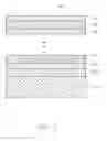
FIG. 1 is a cross-sectional view of an exemplary embodiment of a coated article.
FIG. 2 is an overlook view of an exemplary embodiment of a vacuum sputtering device.
DETAILED DESCRIPTION
FIG. 1 shows a coated article 100 according to an exemplary embodiment. The coated article 100 includes a substrate 10, a combining layer 20 formed on the substrate 10, a plurality of chromium nitride (CrN) layers 30 and a plurality of copper-zinc (Cu—Zn) alloy layers 40 formed on the combining layer 20. Each CrN layer 30 alternates/interleaves with one Cu—Zn alloy layer 40. One of the CrN layers 30 is directly formed on the combining layer 20. Furthermore, one of the CrN layers 30 also forms the outermost layer of the coated article 100. Therefore, there is typically one more CrN layer 30 than there are Cu—Zn alloy layers 40. The total thickness of the CrN layers 30 and the Cu—Zn alloy layers 40 may be of about 1 μm-8 μm. The total number of the CrN layers 30 may be about 5 layers to about 21 layers. The total number of the Cu—Zn alloy layers 40 may be about 4 layers to about 20 layers. As mentioned above, due to one of the CrN layers 30 also forming the outermost layer of the coated article 100, there is typically one more CrN layer 30 than there are Cu—Zn alloy layers 40.
The substrate 10 may be made of stainless steel or chromium (Cr) contained alloys.
The combining layer 20 may be a chromium (Cr) layer formed on the substrate 10 by vacuum sputtering. The combining layer 20 has a thickness of about 100 nm-200 nm.
The CrN layers 30 may be formed by vacuum sputtering. Each CrN layer 30 may have a thickness of about 50 nm-100 nm. The CrN layers 30 have a porous structure, in which a plurality of tiny holes (not shown) are formed. Additionally, the CrN layers 30 are abrasion and corrosion resistant, which provides the coated article 100 good abrasion and corrosion resistance properties. Moreover, the outermost CrN layer 30 provides the coated article 100 colorful appearance.
The Cu—Zn alloy layers 40 may be formed by vacuum sputtering. Each Cu—Zn alloy layer 40 may have a thickness of about 200 nm-300 nm. Each Cu—Zn alloy layer 40 has a portion that imbeds in the porous structure (or the tiny holes) of the adjacent two CrN layers 30. As such, the Cu—Zn alloy layers 40 are securely attached to the CrN layers 30 and the copper ions or zinc ions within the Cu—Zn alloy layers 40 will not be dissolved rapidly, thus the Cu—Zn alloy layers 40 have persisting antibacterial effect. Furthermore, the outermost CrN layer 30 will protect the Cu—Zn alloy layers 40 from abrasion, which further prolongs the antibacterial effect of the coated article 100.
A method for making the coated article 100 may include the following steps:
The substrate 10 is pre-treated, such pre-treating process may include the following steps:
The substrate 10 is cleaned in an ultrasonic cleaning device (not shown) filled with ethanol or acetone.
The substrate 10 is plasma cleaned. Referring to FIG. 2, the substrate 10 may be positioned in a coating chamber 21 of a vacuum sputtering device 200. The coating chamber 21 is fixed with chromium targets 23 and Cu—Zn alloy targets 25. The coating chamber 21 is then evacuated to about 4.0×10⁻³ Pa. Argon gas (Ar) having a purity of about 99.999% may be used as a working gas and is fed into the coating chamber 21 at a flow rate of about 100 standard-state cubic centimeters per minute (sccm) to 300 sccm. The substrate 10 may have a bias voltage of about −200 V to about −800 V, then high-frequency voltage is produced in the coating chamber 21 and the argon gas is ionized to plasma. The plasma then strikes the surface of the substrate 10 to clean the surface of the substrate 10. Plasma cleaning of the substrate 10 may take about 3 minutes (min)-10 min. The plasma cleaning process enhances the bond between the substrate 10 and the combining layer 20. The chromium targets 23 and the Cu—Zn alloy targets 25 are unaffected by the pre-cleaning process.
The combining layer 20 may be magnetron sputtered on the pretreated substrate 10 by using a direct current power for the chromium targets 23. Magnetron sputtering of the combining layer 20 is implemented in the coating chamber 21. The inside of the coating chamber 21 is heated to about 80° C.-150° C. Argon gas may be used as a working gas and is fed into the coating chamber 21 at a flow rate of about 100 sccm-300 sccm. The direct current power is applied to the chromium targets 23, and then chromium atoms are sputtered off from the chromium targets 23 to deposit the combining layer 20 on the substrate 10. During the depositing process, the substrate 10 may have a bias voltage of about −50 V to about −150 V. Depositing of the combining layer 20 may take about 5 min-10 min.
One of the CrN layers 30 may be magnetron sputtered on the combining layer 20 by using a direct current power for the chromium targets 23. Magnetron sputtering of the CrN layer 30 is implemented in the coating chamber 21. The substrate 10 in the coating chamber 21 is heated to about 70° C.-130° C. Nitrogen (N2) may be used as a reaction gas and is fed into the coating chamber 21 at a flow rate of about 10 sccm-20 sccm. Argon gas may be used as a working gas and is fed into the coating chamber 21 at a flow rate of about 20 sccm-50 sccm. The direct current power is applied to the chromium targets 23, and then chromium atoms are sputtered off from the chromium targets 23. The chromium atoms and nitrogen atoms are ionized in an electrical field in the coating chamber 21. The ionized chromium then chemically reacts with the ionized nitrogen to deposit the CrN layer 30 on the combining layer 20. During the depositing process, the substrate 10 may have a direct current bias voltage of about −50 V to about −150 V. Depositing of the CrN layer 30 may take about 2 min-3 min.
One of the Cu—Zn alloy layers 40 may be magnetron sputtered on the CrN layer 30 by using a radio frequency power for the Cu—Zn alloy targets 25. The Cu within the Cu—Zn alloy target 25 has a mass percentage of about 80%-90%. Magnetron sputtering of the Cu—Zn alloy layer 40 is implemented in the coating chamber 21. The substrate 10 in the coating chamber 21 is heated to about 70° C.-130° C. Argon gas may be used as a working gas and is fed into the coating chamber 21 at a flow rate of about 20 sccm-50 sccm. The radio frequency power is applied to the Cu—Zn alloy targets 25, and then Cu atoms and Zn atoms are sputtered off from the Cu—Zn alloy targets 25 to deposit the Cu—Zn alloy layer 40 on the CrN layer 30. During the depositing process, the substrate 10 may have a coupled pulse bias voltage of about −180 V to about −350 V. The coupled pulse bias voltage has a pulse frequency of about 10 KHz and a pulse width of about 20 μs. Depositing of the Cu—Zn alloy layer 40 may take about 2 min-3 min.
The steps of magnetron sputtering the CrN layer 30 and the Cu—Zn alloy layer 40 are repeated for about 3-19 times to form the coated article 100. In this embodiment, one more CrN layer 30 may be vacuum sputtered on the Cu—Zn alloy layer 40 and the CrN layer 30 forms the outermost layer of the coated article 100.
It is believed that the exemplary embodiment and its advantages will be understood from the foregoing description, and it will be apparent that various changes may be made thereto without departing from the spirit and scope of the disclosure or sacrificing all of its advantages, the examples hereinbefore described merely being preferred or exemplary embodiment of the disclosure.
Claims
What is claimed is:1. A coated article, comprising:
a substrate;
a combining layer formed on the substrate, the combining layer being a chromium layer; and
a plurality of alternating chromium nitride and copper-zinc alloy layers formed on the combining layer.
2. The coated article as claimed in claim 1, wherein one of the chromium nitride layers is directly formed on the combining layer; one of the chromium nitride layers forms an outermost layer of the coated article.
3. The coated article as claimed in claim 1, wherein the substrate is made of stainless steel or chromium contained alloys.
4. The coated article as claimed in claim 1, wherein each chromium nitride layer is formed by vacuum sputtering and has a thickness of about 50 nm-100 nm.
5. The coated article as claimed in claim 1, wherein each copper-zinc alloy layer is formed by vacuum sputtering and has a thickness of about 200 nm-300 nm.
6. The coated article as claimed in claim 1, wherein the chromium nitride layers and the copper-zinc alloy layers have a total thickness of about 1 μm-8 μm.
7. The coated article as claimed in claim 1, wherein the combining layer is formed by vacuum sputtering and has a thickness of about 100 nm-200 nm.
8. The coated article as claimed in claim 1, wherein the chromium nitride layers have porous structure.
9. The coated article as claimed in claim 8, wherein each copper-zinc alloy layer has a portion that imbeds in the porous structure of the adjacent chromium nitride layers.
10. The coated article as claimed in claim 1, wherein total number of the chromium nitride layers are about 5 layers to about 21 layers, and total number of the copper-zinc alloy layers are about 4 layers to about 20 layers.
11. A method for making a coated article, comprising:
providing a substrate;
forming a combining layer on the substrate, the combining layer being a chromium layer;
forming a chromium nitride layer on the combining layer by vacuum sputtering, using nitrogen as a reaction gas and using a chromium target;
forming a copper-zinc alloy layer on the chromium nitride layer by vacuum sputtering, using copper-zinc alloy target; and
repeating the steps of alternatingly forming the chromium nitride layer and the copper-zinc alloy layer to form the coated article.
12. The method as claimed in claim 11, wherein forming the chromium nitride layer is by using a magnetron sputtering method; the nitrogen has a flow rate of about 10 sccm-20 sccm; magnetron sputtering of the chromium nitride layer uses argon as a working gas, the argon has a flow rate of about 20 sccm-50 sccm; magnetron sputtering of the chromium nitride layer is conducted at a temperature of about 70° C.-130° C. and takes about 2 min-3 min.
13. The method as claimed in claim 12, wherein the substrate has a direct current bias voltage of about −50V to about −150V during magnetron sputtering of the chromium nitride layer.
14. The method as claimed in claim 11, wherein forming the copper-zinc alloy layer is by using a magnetron sputtering method; the copper-zinc alloy target contains copper having a mass percentage of about 80%-90%; magnetron sputtering of the copper-zinc alloy layer uses argon as a working gas, the argon has a flow rate of about 20 sccm-50 sccm; magnetron sputtering of the copper-zinc alloy layer is conducted at a temperature of about 70° C.-130° C. and takes about 2 min-3 min.
15. The method as claimed in claim 14, wherein the substrate has a coupled pulse bias voltage of about −180V to about −350V during magnetron sputtering of the copper-zinc alloy layer, the coupled pulse bias voltage has a pulse frequency of about 10 KHz and a pulse width of about 20 μs.
16. The method as claimed in claim 11, wherein forming the combining layer is by using a magnetron sputtering method, uses chromium target, uses argon as a working gas, the argon has a flow rate of about 100 sccm-300 sccm; magnetron sputtering of the combining layer is conducted at a temperature of about 80° C.-150° C. and takes about 5 min-10 min.
17. The method as claimed in claim 16, wherein the substrate has a bias voltage of about −50V to about −150V during magnetron sputtering of the combining layer.
18. The method as claimed in claim 11, wherein the step of repeating the forming of the chromium nitride layer and the copper-zinc alloy layer is carried out for about three times to about nineteen times.
19. The method as claimed in claim 18, further comprising a step of forming a chromium nitride layer on the copper-zinc alloy layer by vacuum sputtering after the step of repeating the forming of the chromium nitride layer and the copper-zinc alloy layer.
20. The method as claimed in claim 11, further comprising a step of pre-treating the substrate before forming the combining layer, the pre-treating process comprises ultrasonic cleaning the substrate and plasma cleaning the substrate.
Images & Drawings included:


Sources:
- United States Patent and Trademark Office - verify current appl. status at the USPTO↗
Similar patent applications:
- » 20140154466
Method of making hydrophobic coated article, coated article including hydrophobic coatings, and/or sol compositions for use in the same - » 20160096769
Method of making hydrophobic coated article, coated article including hydrophobic coatings, and/or sol compositions for use in the same - » 10472289
Coated article, coating liquid composition, and method for producing coated article - » 20070100066
COATED ARTICLE, COATING LIQUID COMPOSITION, AND METHOD FOR PRODUCING COATED ARTICLE - » 20140193760
COATED ARTICLE, PROCESS OF COATING AN ARTICLE, AND METHOD OF USING A COATED ARTICLE - » 10397001
Method of making coated articles and coated articles made thereby - » 20090022978
Wax coatings, methods of making coated articles and coated articles therefrom - » 20090022999
SILICONE COATINGS, METHODS OF MAKING SILICONE COATED ARTICLES AND COATED ARTICLES THEREFROM - » 20120251819
Methods of changing the visible light transmittance of coated articles and coated articles made thereby - » 10007382
Method of making coated articles and coated articles made thereby
Recent applications in this class:
- » 20250011914 2025-01-09
COSMETIC FINISH FOR ALUMINUM ALLOYS - » 20240158905 2024-05-16
PROTECTIVE COATING FOR A COPPER ALLOW SUBSTRATE AND CORRESPONDING PROCESS - » 20230193447 2023-06-22
PRECIOUS METAL LAMINATE AND METHODS OF MANUFACTURE - » 20230160052 2023-05-25
SELF-LUBRICATING FILM OVER WIDE TEMPERATURE RANGES IN VACUUM AND PREPARATION METHOD AND USE THEREOF - » 20230126038 2023-04-27
METHOD FOR DECORATING A SUBSTRATE - » 20210340662 2021-11-04
Low friction wear film and method for producing the same - » 20210047719 2021-02-18
Optical element having metallic seed layer and aluminum layer, and method for producing same - » 20210032738 2021-02-04
Multimodal microstructure material and methods of forming same - » 20200270738 2020-08-27
METHOD FOR PRODUCING A BASE PLATE FOR AN ELECTRONIC MODULE - » 20200080185 2020-03-12
Multimodal microstructure material and methods of forming same
Recent applications for this Assignee:
- » 20250218287 2025-07-03
METHOD OF GENERATING AND PROMPTING TRAFFIC INFORMATION, AND ROADSIDE DEVICE THEREOF - » 20250178535 2025-06-05
METHOD FOR CONSTRUCTING 3D PANORAMIC VIEW MODEL, VEHICLE-MOUNTED DEVICE, AND STORAGE MEDIUM - » 20250074444 2025-03-06
METHOD FOR EARLY WARNING A BLIND AREA, ELECTRONIC DEVICE AND STORAGE MEDIUM - » 20240416754 2024-12-19
DISPLAY CONTROL DEVICE, DISPLAY EQUIPMENT, AND VEHICLE EMPLOYING DEVICE - » 20240411051 2024-12-12
Light-emitting device array and optical transceiver system having the same - » 20240324114 2024-09-26
DISPLAY CONTROL DEVICE AND VEHICLE EMPLOYING DEVICE - » 20240295957 2024-09-05
METHOD FOR CONTROLLING ELECTRONIC DEVICE, ELECTRONIC DEVICE AND COMPUTER STROAGE MEDIUM EMPLOYING METHOD - » 20240257357 2024-08-01
METHOD FOR DETECTING OBSTACLES, ELECTRONIC DEVICE, AND STORAGE MEDIUM - » 20240203133 2024-06-20
LANE LINE RECOGNITION METHOD, ELECTRONIC DEVICE AND STORAGE MEDIUM - » 20240194999 2024-06-13
Robot using limiting device for locking battery