Nanolaminated coated cutting tool
US20120114436A1
2012-05-10
13/375,570
2010-05-28
✅ Patent granted
US 8,852,305 B2
2014-10-07
WO; PCT/SE2010/050580; 20100528
WO; WO2010/140958; 20101209
Archene Turner
Young & Thompson
2031-04-10
Abstract:
A cutting tool insert for machining by chip removal includes a body of a hard alloy of cemented carbide, cermet, ceramics, cubic boron nitride based material or high speed steel, onto which a hard and wear resistant coating is deposited by physical vapour deposition. The coating includes a polycrystalline nanolaminated structure of alternating layers A and B where layer A is (Ti,Al,Me1)N and Me1 is optionally one or more of the metal elements from group 3, 4, 5 or 6 in the periodic table, layer B is (Ti,Si,Me2)N and Me2 is optionally one or more of the metal elements from group 3, 4, 5 or 6 in the periodic table including Al with a thickness between 0.5 and 20 μm and method of making the same. This insert is particularly useful in metal cutting applications generating high temperatures with improved edge integrity, machining of super alloys, stainless and hardened steels.
Inventors:
- Mats Johansson 22 🇸🇪 Linkoping, Sweden
- Jon Andersson 16 🇸🇪 Vasteras, Sweden
- Rachid Msaoubi 10 🇸🇪 Fagersta, Sweden
- Hindrik Engstrom 6 🇸🇪 Soderbarke, Sweden
Assignee:
- Seco Tools AB 239 🇸🇪 Fagersta, Sweden
Applicant:
Interested in similar patents?
Get notified when new applications in this technology area are published.
Classification:
C23C28/00 IPC
Coating for obtaining at least two superposed coatings either by methods not provided for in a single one of groups - or by combinations of methods provided for in subclasses and or
Y10T29/49995 » CPC further
Metal working; Method of mechanical manufacture Shaping one-piece blank by removing material
Y10T407/27 » CPC further
Cutters, for shaping comprising tool of specific chemical composition
Y10T428/24975 » CPC further
Stock material or miscellaneous articles; Structurally defined web or sheet [e.g., overall dimension, etc.] including components having same physical characteristic in differing degree; Thickness [relative or absolute]; Absolute thicknesses specified No layer or component greater than 5 mils thick
Y10T428/265 » CPC further
Stock material or miscellaneous articles; Web or sheet containing structurally defined element or component, the element or component having a specified physical dimension; Coating layer not in excess of 5 mils thick or equivalent; Up to 3 mils 1 mil or less
C04B41/4529 » CPC further
After-treatment of mortars, concrete, artificial stone or ceramics; Treatment of natural stone; Coating or impregnating e.g. injection in masonry, partial coating of green or fired ceramics, organic coating compositions for adhering together two concrete elements, characterised by the method of application applied from the gas phase
C04B41/5063 » CPC further
After-treatment of mortars, concrete, artificial stone or ceramics; Treatment of natural stone; Coating or impregnating e.g. injection in masonry, partial coating of green or fired ceramics, organic coating compositions for adhering together two concrete elements, with inorganic materials non-oxide ceramics; Borides, Nitrides or Silicides Aluminium nitride
C04B41/5062 » CPC further
After-treatment of mortars, concrete, artificial stone or ceramics; Treatment of natural stone; Coating or impregnating e.g. injection in masonry, partial coating of green or fired ceramics, organic coating compositions for adhering together two concrete elements, with inorganic materials non-oxide ceramics Borides, Nitrides or Silicides
C04B41/5066 » CPC further
After-treatment of mortars, concrete, artificial stone or ceramics; Treatment of natural stone; Coating or impregnating e.g. injection in masonry, partial coating of green or fired ceramics, organic coating compositions for adhering together two concrete elements, with inorganic materials non-oxide ceramics; Borides, Nitrides or Silicides Silicon nitride
C04B41/5068 » CPC further
After-treatment of mortars, concrete, artificial stone or ceramics; Treatment of natural stone; Coating or impregnating e.g. injection in masonry, partial coating of green or fired ceramics, organic coating compositions for adhering together two concrete elements, with inorganic materials non-oxide ceramics; Borides, Nitrides or Silicides Titanium nitride
C04B35/00 » CPC further
Shaped ceramic products characterised by their composition ; Ceramics compositions ; Processing powders of inorganic compounds preparatory to the manufacturing of ceramic products
C04B35/5831 » CPC further
Shaped ceramic products characterised by their composition ; Ceramics compositions ; Processing powders of inorganic compounds preparatory to the manufacturing of ceramic products based on non-oxide ceramics based on borides, nitrides, or silicides based on boron nitride based on cubic boron nitrides or Wurtzitic boron nitrides, including crystal structure transformation of powder
B23B27/14 IPC
Tools for turning or boring machines ; Tools of a similar kind in general; Accessories therefor Cutting tools of which the bits or tips or cutting inserts are of special material
C23C14/24 IPC
Coating by vacuum evaporation, by sputtering or by ion implantation of the coating forming material characterised by the process of coating Vacuum evaporation
B23P13/00 IPC
Making metal objects by operations essentially involving machining but not covered by a single other subclass
C04B41/009 » CPC further
After-treatment of mortars, concrete, artificial stone or ceramics; Treatment of natural stone characterised by the material treated
C23C14/0641 » CPC further
Coating by vacuum evaporation, by sputtering or by ion implantation of the coating forming material characterised by the coating material Nitrides
C23C28/42 » CPC further
Coating for obtaining at least two superposed coatings either by methods not provided for in a single one of groups - or by combinations of methods provided for in subclasses and or; Coatings including alternating layers following a pattern, a periodic or defined repetition characterized by the composition of the alternating layers
C23C30/005 » CPC further
Coating with metallic material characterised only by the composition of the metallic material, i.e. not characterised by the coating process on hard metal substrates
C23C28/044 » CPC further
Coating for obtaining at least two superposed coatings either by methods not provided for in a single one of groups - or by combinations of methods provided for in subclasses and or only coatings of inorganic non-metallic material coatings specially adapted for cutting tools or wear applications
C23C28/042 » CPC further
Coating for obtaining at least two superposed coatings either by methods not provided for in a single one of groups - or by combinations of methods provided for in subclasses and or only coatings of inorganic non-metallic material including a refractory ceramic layer, e.g. refractory metal oxides, ZrO, rare earth oxides
B23B2222/36 » CPC further
Materials of tools or workpieces composed of metals, alloys or metal matrices Nickel chrome alloys, e.g. Inconel®
B23B2224/24 » CPC further
Materials of tools or workpieces composed of a compound including a metal Titanium aluminium nitride
B23B2228/08 » CPC further
Properties of materials of tools or workpieces, materials of tools or workpieces applied in a specific manner applied by physical vapour deposition [PVD]
B23B2228/10 » CPC further
Properties of materials of tools or workpieces, materials of tools or workpieces applied in a specific manner Coatings
C04B41/89 » CPC further
After-treatment of mortars, concrete, artificial stone or ceramics; Treatment of natural stone of only ceramics; Coating or impregnation for obtaining at least two superposed coatings having different compositions
C23C14/00 IPC
Coating by vacuum evaporation, by sputtering or by ion implantation of the coating forming material
C04B41/00 IPC
After-treatment of mortars, concrete, artificial stone or ceramics; Treatment of natural stone
C04B41/52 » CPC main
After-treatment of mortars, concrete, artificial stone or ceramics; Treatment of natural stone; Coating or impregnating e.g. injection in masonry, partial coating of green or fired ceramics, organic coating compositions for adhering together two concrete elements, Multiple coating or impregnating multiple coating or impregnating with the same composition or with compositions only differing in the concentration of the constituents, is classified as single coating or impregnation
C23C14/06 IPC
Coating by vacuum evaporation, by sputtering or by ion implantation of the coating forming material characterised by the coating material
C23C30/00 IPC
Coating with metallic material characterised only by the composition of the metallic material, i.e. not characterised by the coating process
C23C28/04 IPC
Coating for obtaining at least two superposed coatings either by methods not provided for in a single one of groups - or by combinations of methods provided for in subclasses and or only coatings of inorganic non-metallic material
Description
BACKGROUND OF THE INVENTION
The present invention relates to a cutting tool insert coated with a hard and wear resistant coating comprising a nanolaminated structure based on (Ti,Al)N and (Ti,Si)N layers, respectively. This insert is particularly useful in metal cutting applications generating high temperatures, e.g., machining of super alloys, stainless steels and hardened steels. The coating is grown by physical vapour deposition (PVD) and preferably by cathodic arc evaporation.
U.S. Pat. No. 7,056,602 discloses a cutting tool insert coated with a cubic structured (TiyAlxMe1-x-y)N based layer where Me is one of the elements: Zr, Hf, V, Nb, Ta, Cr, Mo, W or Si, and: x is between 0.50 and 0.80; the ratio, x/(x+y), is between 0.50 and 0.85; the sum of Ti and Al subscripts, x+y, is between 0.7 and 1.0.
EP 1736565 discloses a cutting tool cubic boron nitride based insert coated with a cubic structured (Me,Si)X phase, where Me is one or more of the elements Ti, V, Cr, Zr, Nb, Mo, Hf, Ta and Al, and X is one or more of the elements N, C, O or B
EP 0588350 discloses a hard layer of Ti—Si—N composite material on a body, the layer being deposited using a source of evaporation possessing a composition of TiaSib with a in the range of 75-85 at % and b 15-25 at %.
Coating optimization has also been obtained by applying different concepts of multilayers as; alternating Ti and Al containing layers (U.S. Pat. No. 6,309,738), oxygen and non-oxygen containing layers (U.S. Pat. No. 6,254,984), one of the layers stacked in the multilayer consists itself of a multilayer (U.S. Pat. No. 6,077,596), alternating nitrogen content (U.S. Pat. No. 5,330,853) or using one metastable compound (U.S. Pat. No. 5,503,912) or as aperiodic multilayer (U.S. Pat. No. 6,103,357).
Further improvements in thermal stability and hardness have been achieved by the introduction of Si into TiN- or TiAlN-based coatings. JP 2000-334607 discloses a coated tool with laminated layers comprising TiSi (layer a) and TiAl (layer b) compounds. The (a) layer is selected among nitride, carbonitride, oxynitride and oxycarbonitride containing 10%<Si<60% with a NaCl type crystalline structure. Layer (b) is selected among nitride, carbonitride, oxynitride and oxycarbonitride containing 40%<Al<75% with a NaCl type crystalline structure. The (a) layer and (b) layers are applied alternately and the (b) layer is located just above the surface of the base material.
EP 1939327 discloses a cutting tool comprising a hard coating giving improved crater and flank wear resistance, said coating comprising an aperiodic multilayer X+Y+X+Y+ . . . with average layer thickness of X and Y layers of between 0.1 and 100 nm and with average chemical composition AlaTibSicCrdCeN1-e, where 0<a<0.5, 0.1<b<0.9, 0.01<c<0.17, 0≦d<0.06, a+b+c+d=1, and 0≦e<1.
The trends towards dry-work processes for environmental protection, i.e., metal cutting operation without using cutting fluids (lubricants) and accelerated machining speed with improved process put even higher demands on the characteristics of the tool materials due to an increased tool cutting-edge temperature. In particular, coating stability at high temperatures, e.g., oxidation- and wear-resistance have become even more crucial.
It is an object of the present invention to provide a coated cutting tool yielding improved performance in metal cutting applications at elevated temperatures.
It is a further object of the present invention to provide a coated cutting tool with improved edge integrity.
It has been found that combining layers based on (Ti,Si)N and (Ti,Al)N, respectively, in a nanolaminated coating structure onto a cutting tool insert significantly improves the tool life due to increased crater wear resistance, flank wear resistance and edge integrity, especially in machining operations generating high tool temperatures.
BRIEF DESCRIPTION OF THE DRAWINGS
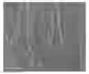
FIG. 1; Scanning electron microscopy (SEM) image showing a fractured cross section of a Ti0.38Al0.62N/Ti0.93Si0.07N nanolaminated structure.
FIG. 2; X-ray diffraction patterns from (a) Ti0.38Al0.62N single layer, (b) Ti0.86Si0.14N single layer, and (c) Ti0.38Al0.62N/Ti0.86Si0.14N nanolaminated structure. The diffraction peaks are indexed as cubic phase (Ti,Si)N (marked with 1), cubic phase (Ti,Al)N (marked with 2) and the peaks originating from the WC or Co (dotted lines).
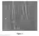
FIG. 3; Scanning electron microscopy (SEM) images showing examples of the cutting edges after 11 minutes of turning in stainless steel showing (a) Ti0.38Al0.62N single layer, (b) Ti0.66Al0.29Si0.05N single layer, and (c) Ti0.38Al0.62N/Ti0.93Si0.07N nanolaminated structure.
DETAILED DESCRIPTION OF THE INVENTION
According to the present invention, there is provided a cutting tool for machining by chip removal comprising a body of a hard alloy of cemented carbide, cermet, ceramics, cubic boron nitride based material or high speed steel, preferably cemented carbide and cermet, onto which is deposited a hard and wear resistant coating comprising a polycrystalline nanolaminated structure of alternating A and B layers with a thickness between 0.5 and 20 μm, preferably between 0.5 and 10 μm, most preferably between 0.5 and 5 μm. Preferably the nanolaminated structure has an overall columnar structure with average column width between 20 and 1000 nm, preferably between 20 and 500 nm, as determined by, e.g., cross section scanning electron microscopy of a middle region of the nanolaminated structure, i.e., in a region within 30 to 70% of the thickness in the growth direction, and said average columnar width is the average from measuring the width of at least ten adjacent columns.
Said layer A is (Ti1-xAlxMe1p)Na, where 0.3<x<0.95, preferably 0.45<x<0.75, and 0.90<a<1.10, preferably 0.96<a<1.04, 0≦p<0.15, and Me1 is one or more of the metal elements from group 3, 4, 5 or 6 in the periodic table, preferably one or more of Zr, Y, V, Nb, Mo and W, most preferably one or more of Zr, Y, V and Nb. Said layer B is (Ti1-y-zSiyMe2z)Nb, where 0.05<y<0.25 preferably 0.05<y<0.18, 0≦z<0.4, 0.9<b<1.1, preferably 0.96<b<1.04, and Me2 is one or more of the metal elements from group 3, 4, 5 or 6 in the periodic table including Al, preferably one or more of Y, V, Nb, Mo, W and Al, most preferably one or more of Y, V, Nb and Al. Layers A and B have an average individual layer thickness between 1 nm and 50 nm, as measured by, e.g., cross sectional transmission electron microscopy of a middle region of the nanolaminated structure, i.e., a region within 30 to 70% of the thickness in the growth direction, and said average layer thickness is the average from measuring the thickness of at least ten adjacent layers. Said nanolaminated structure comprises a phase mixture of cubic and hexagonal phases, preferably only cubic phases, as determined by X-ray diffraction.
In a first preferred embodiment z=p=0.
In a second preferred embodiment Me1 is one or more of Zr, Y, V and Nb with 0<p<0.05.
In a third preferred embodiment Me2 is Y, 0<z<0.15.
In a fourth preferred embodiment Me2 is one or both of V and Nb with 0<z<0.3.
In a fifth preferred embodiment Me2 is Al, 0.2<z<0.4.
Within the nanolaminated structure, Layer A has a stress level of −5.0<a<0 GPa, preferably −3.0<σ<−0.5 GPa.
Said coating may comprise an inner single- and/or multilayer coating of TiN, TiC, Ti(C,N) or (Ti,Al)N, preferably (Ti,Al)N, and/or an outer single- and/or multilayer coating of TiN, TiC, Ti(C,N), (Ti,Si)N or (Ti,Al)N, preferably (Ti,Si)N or (Ti,Al)N, according to prior art, to a total coating thickness, including the thickness of the nanolaminated structure, of between 0.5 and 30 μm, preferably between 0.5 and 15 μm, and most preferably between 0.5 and 10 μm.
The deposition method for the coatings of the present invention is physical vapour deposition (PVD), preferably cathodic arc evaporation, using alloy or composite cathodes under the following conditions; (Ti,Al,Me1)N and (Ti,Si,Me2)N layers are grown from cathodes yielding the desired layer composition. The evaporation current is between 50 A and 200 A. The layers are grown in an Ar+N2 atmosphere, preferably in a pure N2 atmosphere, at a total pressure of 0.5 Pa to 9.0 Pa, preferably 1.5 Pa to 5.0 Pa. The bias is −10 V to −300 V, preferably −20 V to −200V. The deposition temperature is between 350° C. and 700° C., preferably between 400° C. and 650° C.
The invention also relates to the use of cutting tool inserts according to the above for machining of stainless steel, super alloys and hardened steel at cutting speeds of 50-500 m/min, preferably 50-300 m/min, with an average feed of 0.08-0.5 mm/rev, preferably 0.1-0.4 mm/rev, depending on cutting speed and insert geometry.
Example 1
The coatings of Table 1 were deposited by cathodic arc evaporation onto the following inserts:
-
- S1: Cemented carbide with (90 wt % WC+10 wt % Co)
- S2: Cemented carbide with (94 wt % WC+6 wt % Co)
- S3: Seco Tools commercial cermet grade, CM
Before deposition, the inserts were cleaned in ultrasonic baths of an alkali solution and alcohol. The deposition chamber was evacuated to a base pressure of less than 2.0×10⁻³ Pa, after which the inserts were sputter cleaned with Ar ions. The coatings were deposited from alloy or composite cathodes in 99.995% pure N2 atmosphere at a total pressure of 2-6 Pa, using a bias of −20 to −60 V and an evaporation current of 60-200 A at 450° C. The cathodes were selected to yield the composition of Layer A and Layer B, respectively, and mounted on opposing sides of the deposition chamber in order to obtain the nanolaminated structure by fixture rotation. The average individual layer thickness was varied by altering the cathode current (60-200 A) and the rotation speed of the fixture (1-5 rpm). The total coating thickness was about 2 μm for all inserts as measured on the flank face.
FIG. 1 shows a scanning electron microscopy (SEM) image of a Ti0.38Al0.62N/Ti0.93Si0.07N nanolaminated structure (coating 9). The individual layers are clearly seen, indicating minimal intermixing between adjacent layers. The individual layer thickness varies due to a 3-fold fixture rotation and a columnar microstructure extends throughout the nanolaminated structure.
X-ray diffractograms of as-deposited coatings were obtained using Cu Kα radiation and a θ-2θ configuration. FIG. 2 shows (a) Ti0.38Al0.62N single layer (coating 39), (b) Ti0.86Si0.14N single layer (coating 41), and (c) Ti0.38Al0.62N/Ti0.86Si0.14N nanolaminated structure (coating 1). All three coatings display only cubic NaCl crystal structures.
The average residual stress, σ, is shown in Table 1. The stresses were evaluated by XRD measurements using the sin2ψ method. The measurements were performed using CuKα-radiation on the NaCl (422)-reflections. Data was obtained with eleven Ψ-angles (positive and negative), equidistant within a sin2Ψ range of 0 to 0.75)(Ψ=0-60°. The residual stress values were evaluated using a Poisson's ratio of ν=0.22 and Young's modulus of E=450 GPa. For the nanolaminated structures stress values were measured for the (Ti,Al)N layers.
The total average composition of the nanolaminated structure was measured by energy dispersive x-ray spectroscopy (EDS) analysis area using a LEO Ultra 55 scanning electron microscope with a Thermo Noran EDS detector operating at 10 kV. The data were evaluated using the Noran System Six (NSS version 2) software.
Table 1 summarizes the results for the example coatings, both according to the invention and comparative coatings according to prior art.
| TABLE 1 | ||
| Composition Layer A | Composition Layer B | |
| (metal at. %) | (metal at. %) |
| Coating | Description | Ti | Al | Si | Me1 | Ti | Al | Si | Me2*** |
| Inventive | |||||||||
| 1 | TiAlN/TiSiN* | 38 | 62 | 0 | 0 | 86 | 0 | 14 | 0 |
| 2 | TiAlN/TiSiN* | 38 | 62 | 0 | 0 | 86 | 0 | 14 | 0 |
| 3 | TiAlN/TiSiN* | 38 | 62 | 0 | 0 | 86 | 0 | 14 | 0 |
| 4 | TiAlN/TiSiN* | 38 | 62 | 0 | 0 | 86 | 0 | 14 | 0 |
| 5 | TiAlN/TiSiN* | 38 | 62 | 0 | 0 | 86 | 0 | 14 | 0 |
| 6 | TiAlN/TiSiN*,** | 38 | 62 | 0 | 0 | 86 | 0 | 14 | 0 |
| 7 | TiAlN/TiSiN* | 50 | 50 | 0 | 0 | 86 | 0 | 14 | 0 |
| 8 | TiAlN/TiSiN* | 38 | 62 | 0 | 0 | 93 | 0 | 7 | 0 |
| 9 | TiAlN/TiSiN* | 38 | 62 | 0 | 0 | 93 | 0 | 7 | 0 |
| 10 | TiAlN/TiSiN* | 50 | 50 | 0 | 0 | 93 | 0 | 7 | 0 |
| 11 | TiAlN/TiSiYN* | 38 | 62 | 0 | 0 | 84 | 0 | 12 | 4 |
| 12 | TiAlN/TiSiYN* | 38 | 62 | 0 | 0 | 83 | 0 | 9 | 8 |
| 13 | TiAlN/TiSiYN* | 38 | 62 | 0 | 0 | 79 | 0 | 7 | 14 |
| 14 | TiAlN/TiSiVN* | 38 | 62 | 0 | 0 | 82 | 0 | 11 | 7 |
| 15 | TiAlN/TiSiVN* | 38 | 62 | 0 | 0 | 76 | 0 | 9 | 15 |
| 16 | TiAlN/TiSiVN* | 50 | 50 | 0 | 0 | 70 | 0 | 7 | 23 |
| 17 | TiAlN/TiSiNbN* | 38 | 62 | 0 | 0 | 85 | 0 | 10 | 5 |
| 18 | TiAlN/TiSiNbN* | 38 | 62 | 0 | 0 | 78 | 0 | 8 | 14 |
| 19 | TiAlN/TiSiNbN* | 38 | 62 | 0 | 0 | 69 | 0 | 6 | 25 |
| 20 | TiAlN/TiSiAlN* | 38 | 62 | 0 | 0 | 67 | 21 | 12 | 0 |
| 21 | TiAlN/TiSiAlN* | 38 | 62 | 0 | 0 | 55 | 39 | 6 | 0 |
| 22 | TiAlN/TiSiAlN* | 38 | 62 | 0 | 0 | 60 | 32 | 8 | 0 |
| 23 | TiAlYN/TiSiN* | 38 | 61 | 0 | 1 | 86 | 0 | 14 | 0 |
| 24 | TiAlYN/TiSiN* | 37 | 59 | 0 | 4 | 86 | 0 | 14 | 0 |
| 25 | TiAlVN/TiSiN* | 38 | 61 | 0 | 1 | 86 | 0 | 14 | 0 |
| 26 | TiAlVN/TiSiN* | 37 | 59 | 0 | 4 | 86 | 0 | 14 | 0 |
| 27 | TiAlNbN/TiSiN* | 38 | 61 | 0 | 1 | 86 | 0 | 14 | 0 |
| 28 | TiAlNbN/TiSiN* | 37 | 59 | 0 | 4 | 86 | 0 | 14 | 0 |
| 29 | TiAlZrN/TiSiN* | 38 | 61 | 0 | 1 | 86 | 0 | 14 | 0 |
| 30 | TiAlZrN/TiSiN* | 37 | 59 | 0 | 4 | 86 | 0 | 14 | 0 |
| 31 | TiAlZrN/TiSiVN* | 38 | 61 | 0 | 1 | 76 | 0 | 9 | 15 |
| 32 | TiAlZrN/TiSiYN* | 37 | 59 | 0 | 4 | 84 | 0 | 12 | 4 |
| 33 | TiAlVN/TiSiAlN* | 37 | 59 | 0 | 4 | 60 | 32 | 8 | 0 |
| Comparative | |||||||||
| 34 | TiN/TiSiN* | 100 | 0 | 0 | 0 | 86 | 0 | 14 | 0 |
| 35 | TiAlSiN/TiSiN* | 61 | 32 | 7 | 0 | 93 | 0 | 7 | 0 |
| 36 | TiAlN/TiSiN* | 80 | 20 | 0 | 0 | 93 | 0 | 7 | 0 |
| 37 | TiAlN/TiSiN*,** | 38 | 62 | 0 | 0 | 86 | 0 | 14 | 0 |
| 38 | TiN/TiAlSiN*,** | 100 | 0 | 0 | 0 | 61 | 32 | 7 | 0 |
| 39 | TiAlN | 37.6 | 62.4 | 0.0 | 0.0 | 0.0 | 0.0 | 0.0 | 0.0 |
| 40 | TiAlN | 49.6 | 50.4 | 0.0 | 0.0 | 0.0 | 0.0 | 0.0 | 0.0 |
| 41 | TiSiN | 86.4 | 0.0 | 13.6 | 0.0 | 0.0 | 0.0 | 0.0 | 0.0 |
| 42 | TiSiN | 92.8 | 0.0 | 7.2 | 0.0 | 0.0 | 0.0 | 0.0 | 0.0 |
| 43 | TiAlSiN | 61.1 | 32.0 | 6.9 | 0.0 | 0.0 | 0.0 | 0.0 | 0.0 |
| 44 | TiSiN + TiAlN** | 85.9 | 0.0 | 14.1 | 0.0 | 38.0 | 62.0 | 0.0 | 0.0 |
| 45 | TiAlN + TiSiN** | 38.3 | 61.7 | 0.0 | 0.0 | 86.0 | 0.0 | 14.0 | 0.0 |
| σ | ||||
| Average composition | Layer thickn. | (GPa) | ||
| Coat- | (at. %) | (nm) | Layer |
| ing | Description | Ti | Al | Si | Me1 | Me2*** | N | A | B | A |
| Inventive | ||||||||||
| 1 | TiAlN/TiSiN* | 31.9 | 12.6 | 4.1 | 0.0 | 0.0 | 51.4 | 5 | 8 | −0.9 |
| 2 | TiAlN/TiSiN* | 39.1 | 5.7 | 5.6 | 0.0 | 0.0 | 49.6 | 4 | 17 | −0.5 |
| 3 | TiAlN/TiSiN* | 26.1 | 21.2 | 2.2 | 0.0 | 0.0 | 50.4 | 11 | 5 | −1.9 |
| 4 | TiAlN/TiSiN* | 34.3 | 11.8 | 4.5 | 0.0 | 0.0 | 49.4 | 3 | 5 | −0.7 |
| 5 | TiAlN/TiSiN* | 27.9 | 18.5 | 2.9 | 0.0 | 0.0 | 50.6 | 24 | 17 | −2.3 |
| 6 | TiAlN/TiSiN*,** | 31.4 | 14.4 | 3.8 | 0.0 | 0.0 | 50.3 | 7 | 8 | −1.1 |
| 7 | TiAlN/TiSiN* | 33.1 | 13.1 | 3.4 | 0.0 | 0.0 | 50.5 | 10 | 9 | −1.4 |
| 8 | TiAlN/TiSiN* | 35.3 | 13.6 | 1.9 | 0.0 | 0.0 | 49.1 | 6 | 8 | −1.3 |
| 9 | TiAlN/TiSiN* | 32.1 | 16.3 | 1.7 | 0.0 | 0.0 | 50.0 | 9 | 6 | −1.4 |
| 10 | TiAlN/TiSiN* | 38.7 | 10.4 | 2.0 | 0.0 | 0.0 | 48.9 | 5 | 6 | −1.0 |
| 11 | TiAlN/TiSiYN* | 29.5 | 16.7 | 2.8 | 0.0 | 1.0 | 50.1 | 11 | 10 | — |
| 12 | TiAlN/TiSiYN* | 31.9 | 12.8 | 2.6 | 0.0 | 2.3 | 50.4 | 4 | 6 | — |
| 13 | TiAlN/TiSiYN* | 28.7 | 16.7 | 1.6 | 0.0 | 3.3 | 49.8 | 8 | 7 | — |
| 14 | TiAlN/TiSiVN* | 32.5 | 13.9 | 3.1 | 0.0 | 2.0 | 48.5 | 7 | 9 | — |
| 15 | TiAlN/TiSiVN* | 27.0 | 17.7 | 2.1 | 0.0 | 3.3 | 50.0 | 10 | 8 | — |
| 16 | TiAlN/TiSiVN* | 32.4 | 9.5 | 2.1 | 0.0 | 7.1 | 48.8 | 5 | 8 | — |
| 17 | TiAlN/TiSiNbN* | 31.1 | 13.6 | 2.9 | 0.0 | 1.4 | 51.0 | 9 | 12 | — |
| 18 | TiAlN/TiSiNbN* | 27.9 | 16 8 | 1.9 | 0.0 | 3.3 | 50.1 | 8 | 7 | — |
| 19 | TiAlN/TiSiNbN* | 26.1 | 14.3 | 1.6 | 0.0 | 6.6 | 51.3 | 5 | 6 | — |
| 20 | TiAlN/TiSiAlN* | 29.4 | 18.4 | 3.6 | 0.0 | 0.0 | 48.6 | 5 | 8 | — |
| 21 | TiAlN/TiSiAlN* | 22.3 | 25.9 | 1.6 | 0.0 | 0.0 | 50.3 | 5 | 6 | — |
| 22 | TiAlN/TiSiAlN* | 24.5 | 22.6 | 2.1 | 0.0 | 0.0 | 50.7 | 6 | 7 | — |
| 23 | TiAlYN/TiSiN* | 34.0 | 11.9 | 4.2 | 0.4 | 0.0 | 49.8 | 6 | 9 | — |
| 24 | TiAlYN/TiSiN* | 34.4 | 12.3 | 4.2 | 1.0 | 0.0 | 49.1 | 5 | 7 | — |
| 25 | TiAlVN/TiSiN* | 32.6 | 11.7 | 4.2 | 0.4 | 0.0 | 51.5 | 5 | 8 | — |
| 26 | TiAlVN/TiSiN* | 34.7 | 12.6 | 3.9 | 1.0 | 0.0 | 48.8 | 6 | 8 | — |
| 27 | TiAlNbN/TiSiN* | 34.4 | 12.5 | 4.3 | 0.4 | 0.0 | 48.9 | 6 | 9 | — |
| 28 | TiAlNbN/TiSiN* | 34.3 | 11.2 | 4.2 | 1.0 | 0.0 | 50.3 | 5 | 8 | — |
| 29 | TiAlZrN/TiSiN* | 31.7 | 14.4 | 3.9 | 0.5 | 0.0 | 50.1 | 6 | 7 | — |
| 30 | TiAlZrN/TiSiN* | 32.4 | 13.3 | 4.0 | 1.1 | 0.0 | 50.3 | 7 | 9 | — |
| 31 | TiAlZrN/ | 29.3 | 13.0 | 2.6 | 0.4 | 4.3 | 50.8 | 5 | 7 | — |
| TiSiVN* | ||||||||||
| 32 | TiAlZrN/ | 33.8 | 11.3 | 3.7 | 0.9 | 1.2 | 49.9 | 5 | 8 | — |
| TiSiYN* | ||||||||||
| 33 | TiAlVN/ | 23.7 | 22.9 | 2.1 | 0.9 | 0.0 | 51.3 | 6 | 7 | — |
| TiSiAlN* | ||||||||||
| Comparative | ||||||||||
| 34 | TiN/TiSiN* | 45.4 | 0.0 | 4.1 | 0.0 | 0.0 | 50.5 | 9 | 12 | −3.0 |
| 35 | TiAlSiN/TiSiN* | 36.7 | 9.5 | 3.5 | 0.0 | 0.0 | 50.3 | 10 | 7 | −2.1 |
| 36 | TiAlN/TiSiN* | 44.0 | 5.0 | 1.8 | 0.0 | 0.0 | 49.2 | 9 | 9 | −2.5 |
| 37 | TiAlN/TiSiN*,** | 27.6 | 19.2 | 2.7 | 0.0 | 0.0 | 50.6 | 130 | 80 | −2.6 |
| 38 | TiN/TiAlSiN*,** | 39.3 | 8.7 | 1.9 | 0.0 | 0.0 | 50.1 | 110 | 130 | −3.1/ |
| −3.3 | ||||||||||
| 39 | TiAlN | — | — | — | — | — | 50.4 | — | — | −2.7 |
| 40 | TiAlN | — | — | — | — | — | 50.6 | — | — | −2.3 |
| 41 | TiSiN | — | — | — | — | — | 49.5 | — | — | −3.1 |
| 42 | TiSiN | — | — | — | — | — | 49.6 | — | — | −2.4 |
| 43 | TiAlSiN | — | — | — | — | — | 50.0 | — | — | −2.9 |
| 44 | TiSiN + TiAlN** | N (at. %): 51.1/49.5 | 1080 | 1250 | — |
| 45 | TiAlN + TiSiN** | N (at. %): 50.1/50.5 | 1140 | 870 | — |
| *Individual layer compositions are estimated from the corresponding single layers. | |||||
| **Constant individual layer thicknesses. | |||||
| ***Me2 content excluding Al, which has its own column. |
Example 2
Coatings 1-8, 10, 12, 22, 29, 34-45 on S1 inserts were tested under the following conditions:
Geometry: CNMG120408-MF1
Application: Longitudinal turning
Work piece material: AISI 316L
Cutting speed: 230 m/min
Feed: 0.15 mm/rev
Depth of cut: 1.5 mm
Tool life criteria: Flank wear (vb)>0.3 mm
The results are presented in Table 2.
FIG. 3 shows SEM images of used edges after 11 minutes turning with (a) comparative coating 39, (b) comparative coating 43, and (c) inventive coating 8. It is clearly seen that the inventive coating show improved crater and edge wear characteristics.
Example 3
Coatings 1, 4, 6, 15, 33, 37, 39, 41, 45 on S2 inserts were tested under the following conditions:
Geometry: CNMG120408-MF1
Application: Longitudinal turning
Work piece material: Inconel 718
Cutting speed: 70 m/min
Feed: 0.2 mm/rev
Depth of cut: ap=0.5 mm
Tool life criteria: Flank wear (vb)>0.3 mm
The results are presented in Table 2.
Example 4
Coatings 1, 3, 9, 17, 36, 39-45 on S3 inserts were tested under the following conditions:
Geometry: DCMT11T304-F1
Application: Longitudinal turning
Work piece material: DIN 100Cr6
Cutting speed: 250 m/min
Feed: 0.15 mm/rev
Depth of cut: ap=0.5 mm
Tool life criteria: Flank wear (vb)>0.2 mm
The results are presented in Table 2.
| TABLE 2 | |||
| Example 2 | Example 3 | Example 4 |
| Coating | Crater | Edge | Life time (min) | Life time (min) | Life time (min) |
| Inventive | |||||
| 1 | Good | Good/Medium | 15 | 8 | 21 |
| 2 | Good | Medium | 14 | — | — |
| 3 | Good/Medium | Good | 13 | — | 18 |
| 4 | Good | Good/Medium | 14 | 8 | — |
| 5 | Good/Medium | Good/Medium | 15 | — | — |
| 6 | Good | Good/Medium | 13 | 9 | — |
| 7 | Good/Medium | Good/Medium | 12 | — | — |
| 8 | Good | Good | 16 | — | — |
| 9 | — | — | — | — | 21 |
| 10 | Good/Medium | Good | 14 | — | — |
| 12 | Good/Medium | Good/Medium | 15 | — | — |
| 15 | — | — | — | 9 | — |
| 17 | — | — | — | — | 21 |
| 22 | Good | Good | 15 | — | — |
| 29 | Good | Good/Medium | 14 | — | — |
| 33 | — | — | — | 10 | — |
| Comparative | |||||
| 34 | Medium | Good/Medium | 10 | — | — |
| 35 | Good | Poor | 12 | — | — |
| 36 | Medium | Good/Medium | 12 | — | 17 |
| 37 | Good/Medium | Poor | 13 | 7 | — |
| 38 | Good/Medium | Poor | 12 | — | — |
| 39 | Medium/Poor | Good | 11 | 6 | 14 |
| 40 | Poor | Good | 8 | — | 12 |
| 41 | Good | Poor | 9 | 5 | 12 |
| 42 | Good/Medium | Medium/Poor | 9 | — | 15 |
| 43 | Good/Medium | Medium | 12 | — | 15 |
| 44 | Medium | Good/Medium | 7 | — | 17 |
| 45 | Good/Medium | Medium/Poor | 10 | 5 | 15 |
It is obvious from the above examples 2-4 that the inserts according to the invention show an increased tool performance with improved edge and crater wear characteristics.
Claims
1. Cutting tool insert for machining by chip removal comprising a body of a hard alloy of cemented carbide, cermet, ceramics, cubic boron nitride based material or high speed steel, onto which is deposited a hard and wear resistant PVD coating characterised in that said coating comprises a columnar and polycrystalline nanolaminated structure of alternating A and B layers where layer A is (Ti1-xAlxMe1p)Na, with 0.3<x<0.95, preferably 0.45<x<0.75, 0.90<a<1.10, preferably 0.96<a<1.04, 0≦p<0.15, and Me1 is one or more of Zr, Y, V, Nb, Mo and W, and where layer B is (Ti1-y-zSiyMe2z)Nb, with 0.05<y<0.25, preferably
0.05<y<0.18, 0≦z<0.4, 0.9<b<1.1, preferably 0.96<b<1.04, and Me2 is one or more of Y, V, Nb, Mo, W and Al, with a thickness of the nanolaminated structure between 0.5 and 20 μm, preferably between 0.5 and 10 μm, an average column width between 20 and 1000 nm, and an average individual thickness of A and B layers between 1 and 50 nm.
2. Cutting tool insert according to claim 1 characterised in that said nanolaminated structure comprises a phase mixture of cubic and hexagonal phases, preferably only cubic phases, as determined by X-ray diffraction.
3. Cutting tool insert according to claim 1 characterised in that z=p=0.
4. Cutting tool insert according to claim 1 characterised in that said coating comprises an inner single- and/or multilayer coating of TiN, TiC, Ti(C,N) or (Ti,Al)N, preferably (Ti,Al)N, and/or an outer single- and/or multilayer coating of TiN, TiC, Ti(C,N), (Ti,Si)N or (Ti,Al)N, preferably (Ti,Si)N or (Ti,Al)N, to a total coating thickness, including the thickness of the nanolaminated structure, of between 0.5 and 30 μm, preferably between 0.5 and 15 μm.
5. Cutting tool insert according to claim 1 characterised in that said body is cemented carbide or cermet.
6. Method of making a cutting tool insert according to claim 1 characterised in that said coating is deposited by cathodic arc evaporation of alloyed or composite cathodes yielding the desired composition of the (Ti,Al,Me1)N and (Ti,Si,Me2)N layers using an evaporation current between 50 A and 200 A, in an Ar+N2 atmosphere, preferably in a pure N2 atmosphere, at a total pressure of 0.5 Pa to 9.0 Pa, preferably 1.5 Pa to 5.0 Pa, a bias between −10 V and −300 V, preferably between −20 V and −200 V, at 350° C. to 700° C., preferably 400° C. to 650° C.
7. Method for machining of stainless steel, super alloys and hardened steel, which comprises using the cutting tool insert of claim 1 at cutting speeds of 50-500 m/min, preferably 50-300 m/min, with an average feed of 0.08-0.5 mm/rev, preferably 0.1-0.4 mm/rev.
8. Cutting tool insert according to claim 2 characterised in that z=p=0.
Images & Drawings included:


Sources:
- United States Patent and Trademark Office - verify current appl. status at the USPTO↗
Similar patent applications:
- » 20120114437
Nanolaminated coated cutting tool - » 20150023751
Nanolaminated coated cutting tool
Recent applications in this class:
- » 20240417339 2024-12-19
CMC materials with integrated thermocouple - » 20240417338 2024-12-19
PART MADE OF COMPOSITE MATERIAL, HAVING CONTROLLED CREEP - » 20240376018 2024-11-14
METHOD FOR PROTECTING A CARBON/CARBON COMPOSITE MATERIAL PART FROM OXIDATION - » 20240228389 2024-07-11
A METHOD FOR PRODUCING CERAMIC TILES, AND CERAMIC TILES - » 20240043350 2024-02-08
CERAMIC MATRIX COMPOSITE ARTICLE AND METHOD OF MAKING THE SAME - » 20230150893 2023-05-18
POROUS CERAMIC LAMINATE AND PROCESS FOR PRODUCING THE SAME - » 20210269370 2021-09-02
Antimicrobial Glaze and Porcelain Enamel via Double Layer Glaze with High Zinc Content - » 20210155558 2021-05-27
Slurry infiltration heat treatment method - » 20200331817 2020-10-22
Component protected by an environmental barrier - » 20200277237 2020-09-03
Compositions for erosion and molten dust resistant environmental barrier coatings
Recent applications for this Assignee:
- » 20240173787 2024-05-30
TOOL AND MANUFACTURING METHOD OF IT - » 20240109138 2024-04-04
Cutting insert and milling tool - » 20230205162 2023-06-29
Tool part, system, method, and a computer program for determining a dimension of the tool part - » 20230196043 2023-06-22
Tool part, system, method and computer program product for determining a tool wear - » 20230158577 2023-05-25
Anvil with curved passage for cutting tool - » 20230130145 2023-04-27
Rotary cutting tool with continuous major flutes and discontinuous minor flutes intersecting to form quadrilateral-shaped face portions - » 20230067286 2023-03-02
Cutting insert - » 20220410280 2022-12-29
CUTTING TOOL ASSEMBLY - » 20220212268 2022-07-07
System and method for tracing the use of a cutting edge - » 20220176471 2022-06-09
Cutting tool, a method for manufacturing a cutting tool and a method for machining of a workpiece