Circuit for controlling non-signal of flat panel display device
US20120127137A1
2012-05-24
13/298,952
2011-11-17
✅ Patent granted
US 9,035,925 B2
2015-05-19
-
-
Robin Mishler
Kile Park Reed & Houtteman PLLC
2033-08-02
Abstract:
Disclosed is a technique, in which when driving chips are used in which control units are respectively merged in driving devices, all modes of the other driving chips are simultaneously converted into a fail safe mode when one driving chip detects a non-signal state. A circuit for controlling a non-signal of a flat panel display device includes a plurality of driving chips. When detecting a non-signal state that the normal signal (LVDS) is not inputted from an outside, each of the plurality of driving chips simultaneously changes potentials of non-signal detection pads of its own driving chip and another driving chip so that all the driving chips are operated in the fail safe mode
Inventors:
- Joon Ho Na 53 🇰🇷 Daejeon-si, South Korea
- Young-Gi KIM 3 🇰🇷 Daejeon-si, South Korea
- Byung-Min Kim 1 🇰🇷 Cheong-si, South Korea
- Young-Gi Kim 1 🇰🇷 Yuseong-gu, South Korea
- Dong-Yun Jeong 1 🇰🇷 Cheong-si, South Korea
Assignee:
- SILICON WORKS CO., LTD 168 🇰🇷 Daejeon-si, South Korea
Applicant:
Interested in similar patents?
Get notified when new applications in this technology area are published.
Classification:
G09G3/006 » CPC further
Control arrangements or circuits, of interest only in connection with visual indicators other than cathode-ray tubes Electronic inspection or testing of displays and display drivers, e.g. of LED or LCD displays
G09G2310/0281 » CPC further
Command of the display device; Addressing, scanning or driving the display screen or processing steps related thereto; Details of driving circuits Arrangement of scan or data electrode driver circuits at the periphery of a panel not inherent to a split matrix structure
G09G2310/0294 » CPC further
Command of the display device; Addressing, scanning or driving the display screen or processing steps related thereto; Details of driving circuits Details of sampling or holding circuits arranged for use in a driver for data electrodes
G09G2310/0297 » CPC further
Command of the display device; Addressing, scanning or driving the display screen or processing steps related thereto; Details of driving circuits Special arrangements with multiplexing or demultiplexing of display data in the drivers for data electrodes, in a pre-processing circuitry delivering display data to said drivers or in the matrix panel, e.g. multiplexing plural data signals to one D/A converter or demultiplexing the D/A converter output to multiple columns
G09G2310/08 » CPC further
Command of the display device Details of timing specific for flat panels, other than clock recovery
G09G2330/028 » CPC further
Aspects of power supply; Aspects of display protection and defect management; Details of power systems and of start or stop of display operation Generation of voltages supplied to electrode drivers in a matrix display other than LCD
G09G2370/08 » CPC further
Aspects of data communication Details of image data interface between the display device controller and the data line driver circuit
G09G2370/14 » CPC further
Aspects of data communication Use of low voltage differential signaling [LVDS] for display data communication
G06F3/038 IPC
Input arrangements for transferring data to be processed into a form capable of being handled by the computer; Output arrangements for transferring data from processing unit to output unit, e.g. interface arrangements; Input arrangements or combined input and output arrangements for interaction between user and computer; Arrangements for converting the position or the displacement of a member into a coded form; Pointing devices displaced or positioned by the user, e.g. mice, trackballs, pens or joysticks ; Accessories therefor Control and interface arrangements therefor, e.g. drivers or device-embedded control circuitry
G09G5/00 » CPC main
Control arrangements or circuits for visual indicators common to cathode-ray tube indicators and other visual indicators
G09G3/00 IPC
Control arrangements or circuits, of interest only in connection with visual indicators other than cathode-ray tubes
G09G3/32 IPC
Control arrangements or circuits, of interest only in connection with visual indicators other than cathode-ray tubes for presentation of an assembly of a number of characters, e.g. a page, by composing the assembly by combination of individual elements arranged in a matrix no fixed position being assigned to or needed to be assigned to the individual characters or partial characters using controlled light sources using electroluminescent panels semiconductive, e.g. using light-emitting diodes [LED]
G09G3/36 IPC
Control arrangements or circuits, of interest only in connection with visual indicators other than cathode-ray tubes for presentation of an assembly of a number of characters, e.g. a page, by composing the assembly by combination of individual elements arranged in a matrix no fixed position being assigned to or needed to be assigned to the individual characters or partial characters by control of light from an independent source using liquid crystals
G09G3/3266 » CPC further
Control arrangements or circuits, of interest only in connection with visual indicators other than cathode-ray tubes for presentation of an assembly of a number of characters, e.g. a page, by composing the assembly by combination of individual elements arranged in a matrix no fixed position being assigned to or needed to be assigned to the individual characters or partial characters using controlled light sources using electroluminescent panels semiconductive, e.g. using light-emitting diodes [LED] organic, e.g. using organic light-emitting diodes [OLED] Details of drivers for scan electrodes
G09G3/3275 » CPC further
Control arrangements or circuits, of interest only in connection with visual indicators other than cathode-ray tubes for presentation of an assembly of a number of characters, e.g. a page, by composing the assembly by combination of individual elements arranged in a matrix no fixed position being assigned to or needed to be assigned to the individual characters or partial characters using controlled light sources using electroluminescent panels semiconductive, e.g. using light-emitting diodes [LED] organic, e.g. using organic light-emitting diodes [OLED] Details of drivers for data electrodes
G09G3/3611 » CPC further
Control arrangements or circuits, of interest only in connection with visual indicators other than cathode-ray tubes for presentation of an assembly of a number of characters, e.g. a page, by composing the assembly by combination of individual elements arranged in a matrix no fixed position being assigned to or needed to be assigned to the individual characters or partial characters by control of light from an independent source using liquid crystals Control of matrices with row and column drivers
G09G3/3655 » CPC further
Control arrangements or circuits, of interest only in connection with visual indicators other than cathode-ray tubes for presentation of an assembly of a number of characters, e.g. a page, by composing the assembly by combination of individual elements arranged in a matrix no fixed position being assigned to or needed to be assigned to the individual characters or partial characters by control of light from an independent source using liquid crystals; Control of matrices with row and column drivers using an active matrix Details of drivers for counter electrodes, e.g. common electrodes for pixel capacitors or supplementary storage capacitors
G09G3/3674 » CPC further
Control arrangements or circuits, of interest only in connection with visual indicators other than cathode-ray tubes for presentation of an assembly of a number of characters, e.g. a page, by composing the assembly by combination of individual elements arranged in a matrix no fixed position being assigned to or needed to be assigned to the individual characters or partial characters by control of light from an independent source using liquid crystals; Control of matrices with row and column drivers Details of drivers for scan electrodes
G09G3/3685 » CPC further
Control arrangements or circuits, of interest only in connection with visual indicators other than cathode-ray tubes for presentation of an assembly of a number of characters, e.g. a page, by composing the assembly by combination of individual elements arranged in a matrix no fixed position being assigned to or needed to be assigned to the individual characters or partial characters by control of light from an independent source using liquid crystals; Control of matrices with row and column drivers Details of drivers for data electrodes
G09G3/3696 » CPC further
Control arrangements or circuits, of interest only in connection with visual indicators other than cathode-ray tubes for presentation of an assembly of a number of characters, e.g. a page, by composing the assembly by combination of individual elements arranged in a matrix no fixed position being assigned to or needed to be assigned to the individual characters or partial characters by control of light from an independent source using liquid crystals; Control of matrices with row and column drivers Generation of voltages supplied to electrode drivers
G09G2300/0408 » CPC further
Aspects of the constitution of display devices; Structural and physical details of display devices; Matrix technologies Integration of the drivers onto the display substrate
G09G2300/043 » CPC further
Aspects of the constitution of display devices; Structural and physical details of display devices; Structural details of the set of electrodes Compensation electrodes or other additional electrodes in matrix displays related to distortions or compensation signals, e.g. for modifying TFT threshold voltage in column driver
G09G2310/0259 » CPC further
Command of the display device; Addressing, scanning or driving the display screen or processing steps related thereto; Details of the generation of driving signals with use of an analog or digital ramp generator in the column driver or in the pixel circuit
G09G2310/0267 » CPC further
Command of the display device; Addressing, scanning or driving the display screen or processing steps related thereto; Details of driving circuits Details of drivers for scan electrodes, other than drivers for liquid crystal, plasma or OLED displays
G09G2310/027 » CPC further
Command of the display device; Addressing, scanning or driving the display screen or processing steps related thereto; Details of driving circuits Details of drivers for data electrodes, the drivers handling digital grey scale data, e.g. use of D/A converters
G09G2310/0272 » CPC further
Command of the display device; Addressing, scanning or driving the display screen or processing steps related thereto; Details of driving circuits Details of drivers for data electrodes, the drivers communicating data to the pixels by means of a current
G09G2310/0275 » CPC further
Command of the display device; Addressing, scanning or driving the display screen or processing steps related thereto; Details of driving circuits Details of drivers for data electrodes, other than drivers for liquid crystal, plasma or OLED displays, not related to handling digital grey scale data or to communication of data to the pixels by means of a current
G09G2310/0283 » CPC further
Command of the display device; Addressing, scanning or driving the display screen or processing steps related thereto; Details of driving circuits Arrangement of drivers for different directions of scanning
G09G2310/067 » CPC further
Command of the display device; Details of flat display driving waveforms Special waveforms for scanning, where no circuit details of the gate driver are given
Description
BACKGROUND OF THE INVENTION
1. Field of the Invention
The present invention relates to a technique for controlling a non-signal of a flat panel display device, and more particularly, to a circuit for controlling a non-signal of a flat panel display device, in which when driving chips are used in which control units are respectively merged in driving devices, all modes of the other driving chips are simultaneously converted into a fail safe mode when one driving chip detects a non-signal state.
2. Description of the Related Art
Recently, flat panel display devices such as a liquid crystal display (LCD), a plasma display panel (PDP) and an organic light emitting diode (OLED) panel have been widely spread and used. Among these flat panel display devices, the LCD has been more widely spread.
FIG. 1 is a block diagram of a related art LCD.
Referring to FIG. 1, the related art LCD includes a liquid crystal panel 110, a timing controller, a plurality of source driver integrated circuits (ICs) 130A to 130C, and a gate driver IC 140.
The liquid crystal panel 110 has a plurality of pixels arrayed in a matrix form at intersection areas of a plurality of data lines and a plurality of gate lines. A transistor formed in each of the pixels provides a data voltage inputted from the data lines to liquid crystal cells in response to a scan signal supplied from a corresponding gate line. A storage capacitor is formed in each of the liquid crystal cells. The storage capacitor performs a function of constantly maintaining the voltage of the liquid crystal cell. Accordingly, an image is displayed on the liquid crystal panel 110.
The timing controller 120 is mounted on a main board separated from the liquid crystal panel 110 so as to generate a gate control signal for controlling the gate driver IC 140 and a data control signal for controlling the source driver ICs 130A to 130C using vertical/horizontal synchronization signals and a clock signal, which are supplied from a system. The timing controller 120 realigns low-voltage differential signaling (LVDS) that is digital video data (RGB) inputted from the system, and supplies the realigned LVDS to the source driver ICs 130A to 130C.
The source driver ICs 130A to 130C are generally attached to one edge of the liquid crystal panel 110. The source driver ICs 130A to 130C convert the digital video data (RGB) into a data voltage corresponding to the grayscale value of the digital video data (RGB) in response to the data control signal supplied from the timing controller 120, and supply the converted data voltage to the data lines of the liquid crystal panel 110.
The gate driver IC 140 is generally attached to the other edge of the liquid crystal panel 110. The gate driver IC 140 sequentially supplies a scan signal to the gate lines in response to the gate control signal supplied from the timing controller 120, so that horizontal lines of the liquid crystal panel 110, to which data is supplied, are selectively driven.
In a system using a method in which one timing controller 120 receives the LVDS from the outside thereof and provides the received LVDS to a plurality of source driver ICs 130A to 130C, the timing controller 120 checks a non-signal state the LVDS is not inputted thereto and simultaneously inform the source driver ICs 130A to 130C that the timing controller 120 is currently in the non-signal state. Thus, the plurality of source driver ICs 130A to 130C can simultaneously operate in a non-signal mode (fail safe mode).
In order to satisfy requirements of large-size and slimness of the LCD, a semiconductor chip has recently been developed, in which timing controllers are merged in source driver ICs, respectively.
When source driver ICs (hereinafter, referred to as ‘driving chips’) having timing controllers merged therein are used, each of the driving chips generates image data and a gate line control signal using an internal oscillator. However, frequencies of signals generated by the respective driving chips are slightly different from each other.
Therefore, in a case where the driving chips are in a non-signal state at the same time, the difference between times at which the respective driving chips sense the non-signal state is generated by the difference in frequency between the internal oscillators. FIG. 2 is a waveform diagram illustrating its example.
For example, it is assumed that first to third driving chips are used, the frequency of an oscillator used in the first driving chip is fastest, the frequency of an oscillator used in the second driving chip is slower than that in the first driving chip and faster than that in the third driving chip, and the frequency of an oscillator used in the third driving chip is slowest. In this case, as shown in (a) to (c) of FIG. 2, the first driving chip first detects the non-signal state, the second driving chip then detects the non-signal state, and the third driving chip finally detects the non-signal state. (d) of FIG. 2 illustrates a time at which the first to third driving chips are all in the non-signal state.
As described above, in the related art flat panel display device using TMIC driving chips, the difference between times at which the respective driving chips sense the non-signal state is generated by the difference in frequency between internal oscillators of the driving chips. Hence, all the driving chips do not simultaneously operate in a fail safe mode, and therefore, the system is not stabilized at a corresponding time.
SUMMARY OF THE INVENTION
Accordingly, the present invention has been made in an effort to solve the problems occurring in the related art, and an object of the present invention is to provide a circuit for controlling a non-signal of a flat panel display device, in which when driving chips are used in which control units are respectively merged in driving devices, all modes of the other driving chips are simultaneously converted into a fail safe mode when an arbitrary driving chip detects a non-signal state.
In order to achieve the above object, according to one aspect of the present invention, there is provided a circuit for controlling a non-signal of a flat panel display device, the circuit including: a plurality of driving chips each configured to have a timing controller and a source driver and allow its own driving chip and another driving chip to be simultaneously operated in a fail safe mode when detecting a non-signal state that a normal signal is not inputted from an outside; and a display panel configured to display an image by being driven by a data voltage corresponding to the grayscale value of data inputted from the plurality of driving chips.
BRIEF DESCRIPTION OF THE DRAWINGS
The above objects, and other features and advantages of the present invention will become more apparent after a reading of the following detailed description taken in conjunction with the drawings, in which:
FIG. 1 is a block diagram of a related art LCD;
(a) to (d) of FIG. 2 are waveform diagrams illustrating an example of detecting non-signal states in a plurality of driving chips;
FIG. 3 is a block diagram of a circuit for controlling a non-signal of a flat panel display device according to an embodiment of the present invention; and
FIG. 4 is a detailed block diagram of driving chips illustrated in FIG. 3.
DETAILED DESCRIPTION OF PREFERRED EMBODIMENTS
Reference will now be made in greater detail to a preferred embodiment of the invention, an example of which is illustrated in the accompanying drawings. Wherever possible, the same reference numerals will be used throughout the drawings and the description to refer to the same or like parts.
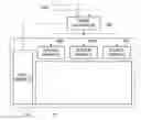
FIG. 3 is a block diagram of a circuit for controlling a non-signal of a flat panel display device according to an embodiment of the present invention.
Referring to FIG. 3, the flat panel display device according to this embodiment includes first to third driving chips 310A to 310C and a display panel 320.
The first to third driving chips 310A to 310C are semiconductor chips (TMIC) in which control units are merged in driving devices, respectively. For example, in a case where the flat panel display panel is an LCD, the control unit corresponds to a timing controller, and the driving device corresponds to a source driver. In this case, the first to third driving chips 310A to 310C align digital video data (RGB) inputted from the outside thereof and convert the aligned digital video data (RGB) into a data voltage corresponding to the grayscale value of the digital video data (RGB). Then, the first to third driving chips 310A to 310C supply the converted data voltage to data lines of the display panel 320. The video data may be transmitted using a low-voltage differential signaling (LVDS) method.
The display panel 320 includes an LCD, a PDP and an OLED panel. For example, in a case where the display panel 320 is a liquid crystal panel, the liquid crystal panel has a plurality of pixels arrayed in a matrix form at intersection areas of a plurality of data lines and a plurality of gate lines. A transistor formed in each of the pixels provides a data voltage inputted from the data lines to liquid crystal cells in response to a scan signal supplied from a corresponding gate line, thereby displaying an image on the liquid crystal panel.
Each of the first to third driving chips 310A to 310C uses a separate internal oscillator. The oscillation frequencies of the oscillators are slightly different from one another depending on conditions in a fabricating process or changes in ambient environment. Therefore, although the first to third driving chips 310A to 310C are simultaneously in a non-signal state that LVDS is not inputted to the control units, the difference between times at which at which the respective driving chips sense the non-signal state is generated by the difference in frequency between the internal oscillators. Here, the non-signal state includes a state that power is applied but a signal (vertical synchronization signal, horizontal synchronization signal, data enable signal, clock signal or the like) is not inputted.
However, when an arbitrary one of the first to third driving chips 310A to 310C first detects the non-signal state that the LVDS is not inputted to the control unit, all the driving chips 310a to 310C are simultaneously operated in a fail safe mode, and thus a side effect due to the difference in frequency does not occur. This will be described in detail with reference to FIG. 4.
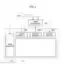
FIG. 4 is a detailed block diagram illustrating an implementation example of the first to third driving chips 310A to 310C illustrated in FIG. 3. As shown in this figure, the first driving chip 310A includes an oscillator 311A, a non-signal detector 312A and a transistor M1, and the second driving 310B includes an oscillator 311B, a non-signal detector 312B and transistor M2. The third driving chip 310C includes an oscillator 311C, a non-signal detector 312C and a transistor M3. Here, the first to third driving chips 310A to 310C have the same structure.
In each of the first to third driving chips 310A to 310C, each of the non-signal detectors 312A to 312C checks a non-signal state that the LVDS is not inputted using a clock signal outputted from each of the oscillators 311A to 311C used only therefor, and outputs a detection signal INT_DET corresponding to the non-signal state.
For example, an operation of detecting a non-signal of the first driving chip 310A will be described. The non-signal detector 312A checks the presence of non-signal state that a normal signal LVDS is not inputted using a clock signal outputted from the oscillator 311A. In a case where the non-signal state is not checked, the non-signal detector 312A outputs the detection signal INT_DET as a ‘low’ signal. Accordingly, the transistor M1 is maintained in an off state. Thus, a non-signal detection pad DET1 is maintained as ‘high.’
On the other hand, the non-signal detector 312A checks the presence of non-signal state that the normal signal LVDS is not inputted as described above. In a case where the non-signal state is checked, the non-signal detector 312A outputs the detection signal INT_DET as a ‘high’ signal. Accordingly, the transistor M1 is turned on. Thus, the voltage of power terminal VCC, supplied to the non-signal detection pad DET through a resistor R1, is muted to a ground terminal through the transistor M1, and therefore, the state of the non-signal detection pad DET1 is changed into a ‘low’ state.
Like the first driving chip 310A, each of the second and second driving chips 310B and 310C checks the presence of non-signal state. In a case where the non-signal state is checked, the state of a non-signal detection pad DET2 or DET3 is changed into a ‘low’ state.
However, the frequencies of clock signals respectively outputted from the oscillators 311A to 311C used in the first to third driving chips 310A to 310C are slightly different as described above. Therefore, in a case where the first to third driving chips 310A to 310C are simultaneously in the non-signal state, the difference between times at which the respective driving chips 310A to 310C sense the non-signal state is generated by the difference in frequency between the oscillators 311A to 311C. FIG. 2 is a waveform diagram illustrating its example.
For example, it is assumed that the frequency of the oscillator 311A used in the first driving chip 310A is fastest, the frequency of the oscillator 311B used in the second driving chip 310B is slower than that in the first driving chip 310A and faster than that in the third driving chip 310C, and the frequency of the oscillator 311C used in the third driving chip 310C is slowest. In this case, as illustrated in (a) to (c) of FIG. 2, the first driving chip first 310A detects the non-signal state, the second driving chip 310B then detects the non-signal state, and the third driving chip 310C finally detects the non-signal state.
However, when an arbitrary one of the first to third driving chips 310A to 310C detects the non-signal state as described above, the state of a corresponding non-signal detection pad among the non-signal detection pads DET1 to DET3 is changed into a ‘low’ state. As illustrated in FIG. 4, the non-signal detection pads DET1 to DET3 are commonly connected through a detection wire, and the commonly connected point is connected to the power terminal VCC through the resistor R1.
Thus, when an arbitrary one of the first to third driving chips 310A to 310C detects the non-signal state, the states of the non-signal detection pads DET1 to DET3 are simultaneously changed into a ‘low’ state. Accordingly, the first to third driving chips 310A to 310C are simultaneously operated in a fail safe mode at the time when an arbitrary one of the first to third driving chips 310A to 310C detects the non-signal state.
The ‘low’ level of the non-signal detection pads DET1 to DET3 can be used for the first to third driving chips 310A to 310C to synchronize a horizontal synchronization signal, vertical synchronization signal, data enable signal, or the like.
(d) of FIG. 2 illustrates a time at which the first to third driving chips 310A to 310C are simultaneously in the non-signal state. At this time, the first to third driving chips 310A to 310C are simultaneously operated in the fail safe mode.
As is apparent from the above description, the present invention provides a circuit for controlling a non-signal of a flat panel display device, in which when driving chips are used in which control units are respectively merged in driving devices, all modes of the other driving chips are simultaneously converted into a fail safe mode when an arbitrary driving chip detects a non-signal state, so that is possible to prevent a system from being in an unstable state in the conversion into the fail safe mode.
Although a preferred embodiment of the present invention has been described for illustrative purposes, those skilled in the art will appreciate that various modifications, additions and substitutions are possible, without departing from the scope and the spirit of the invention as disclosed in the accompanying claims.
Claims
What is claimed is:1. A circuit for controlling a non-signal of a flat panel display device, the circuit comprising:
a plurality of driving chips each configured to have a timing controller and a source driver and allow its own driving chip and another driving chip to be simultaneously operated in a fail safe mode when detecting a non-signal state that a normal signal is not inputted from an outside; and
a display panel configured to display an image by being driven by a data voltage corresponding to the grayscale value of data inputted from the plurality of driving chips.
2. The circuit of claim 1, wherein, when detecting the non-signal state that the normal signal is not inputted from the outside, each of the plurality of driving chips simultaneously changes potentials of non-signal detection pads of its own driving chip and another driving chip so that all the driving chips are operated in the fail safe mode.
3. The circuit of claim 2, wherein the non-signal detection pads of its own driving chip and another driving chip are commonly connected to each other, and the commonly connected point is connected to a power terminal.
4. The circuit of claim 1, wherein each of the plurality of driving chips comprises:
an oscillator configured to generate a clock signal;
a non-signal detector configured to detect the non-signal state that the normal signal is not inputted using the clock signal outputted from the oscillator and outputs a signal having a logic corresponding to the non-signal state; and
a transistor configured to be turned on by the signal outputted when the non-signal detector detects the non-signal state so as to simultaneously change potentials of the non-signal detection pads of its own driving chip and another driving chip.
5. The circuit of claim 1, wherein, in the plurality of driving chips, the driving chip using the oscillator that generates a clock signal having a frequency higher than that outputted from the oscillator of another driving chip first detects the non-signal state.
6. A circuit for controlling a non-signal of a flat panel display device, the circuit comprising first and second driving chips in which each timing controller and each source driver are merged, wherein:
the first driving chip comprises a first oscillator for generating a first clock, a first signal detector for monitoring the presence of inputting of a normal signal using the first clock and enabling a first control signal when the normal signal is not inputted, and a first transistor having one terminal connected to a ground terminal and the other terminal connected to a first detection pad, the first transistor connecting the first detection pad to the ground terminal in response to the first control signal;
the second driving chip comprises a second oscillator for generating a second clock, a second signal detector for monitoring the presence of inputting of the normal signal using the second clock and enabling a second control signal when the normal signal is not inputted, and a second transistor having one terminal connected to the ground terminal and the other terminal connected to a second detection pad, the second transistor connecting the second detection pad to the ground terminal in response to the second control signal; and
the first and second detection pads are commonly connected through a detection wire.
Images & Drawings included:


Sources:
- United States Patent and Trademark Office - verify current appl. status at the USPTO↗
Recent applications in this class:
- » 20250014535 2025-01-09
ACCELERATED FRAME TRANSMISSION - » 20240296812 2024-09-05
Window and display device including the same - » 20240233678 2024-07-11
CONTROL METHOD, APPARATUS, AND STORAGE MEDIUM - » 20230402020 2023-12-14
SYSTEMS AND METHODS FOR PROVIDING INTEGRATED DIGITAL SIGNAGE ADVERTISING TO ELECTRONIC SHELF EDGE LABELS AND SYSTEMS THEREOF - » 20230252732 2023-08-10
Systems and Methods for Identifying Threats and Locations, Systems and Method for Augmenting Real-Time Displays Demonstrating the Threat Location, and Systems and Methods for Responding to Threats - » 20230148254 2023-05-11
Accelerated frame transmission - » 20220328017 2022-10-13
ELECTRONIC DEVICE AND METHOD OF PROCESSING NOTIFICATION IN ELECTRONIC DEVICE - » 20220180837 2022-06-09
APPARATUS, METHOD AND STORAGE MEDIUM - » 20210407456 2021-12-30
Accelerated frame transmission - » 20210142759 2021-05-13
Smart mirror, device and method for controlling screen state of electronic device, and storage medium
Recent applications for this Assignee:
- » 20210005136 2021-01-07
Driver for display device - » 20200211429 2020-07-02
Mura correction system - » 20200202765 2020-06-25
Source driving circuit - » 20200152107 2020-05-14
Display driving device - » 20200128643 2020-04-23
Vehicle lamp control apparatus - » 20200111444 2020-04-09
Display device, and source driver and packet recognition method thereof - » 20200035143 2020-01-30
Source driver for display apparatus - » 20200027824 2020-01-23
Flexible circuit board for display - » 20190385504 2019-12-19
Display driving device and display device including the same - » 20190339808 2019-11-07
Display device and driver thereof