Ionic junction for radiation detectors
US20120153295A1
2012-06-21
13/034,772
2011-02-25
✅ Patent granted
US 8,723,186 B2
2014-05-13
-
-
Mark Tornow | Priya Rampersaud
Sam Pasternack | MIT Technology Licensing Office
2031-04-19
Abstract:
Radiation detector. The detector includes an ionic junction having an ionically bonded wide band gap material having a first region dominated by positively charged ionic defects in intimate contact with a second region dominated by negatively charged ionic defects forming depleted regions on both sides of the junction resulting in a built-in electric field. The detector also includes an ionic junction having a first ionically bonded wide band gap material dominated by positively charged ionic defects in intimate contact with a second ionically bonded wide band gap material dominated by negatively charged ionic defects forming depleted regions on both sides of the junction resulting in a built-in electric field. Circuit means are provided to establish a voltage across the junction so that radiation impinging upon the junction will cause a current to flow in the circuit.
Inventors:
- Harry L. Tuller 26 🇺🇸 Wellesley, MA, United States
- Sean R. Bishop 1 🇺🇸 Somerville, MA, United States
Assignee:
- MASSACHUSETTS INSTITUTE OF TECHNOLOGY 7,186 🇺🇸 Cambridge, MA, United States
Applicant:
Interested in similar patents?
Get notified when new applications in this technology area are published.
Classification:
C01G15/00 » CPC main
Compounds of gallium, indium or thallium
C01G21/16 » CPC further
Compounds of lead Halides
C01G21/21 » CPC further
Compounds of lead Sulfides
C30B11/00 » CPC further
Single-crystal growth by normal freezing or freezing under temperature gradient, e.g. Bridgman-Stockbarger method
C30B29/12 » CPC further
Single crystals or homogeneous polycrystalline material with defined structure characterised by the material or by their shape; Inorganic compounds or compositions Halides
C01P2006/40 » CPC further
Physical properties of inorganic compounds Electric properties
H01L31/0264 IPC
Semiconductor devices sensitive to infra-red radiation, light, electromagnetic radiation of shorter wavelength or corpuscular radiation and specially adapted either for the conversion of the energy of such radiation into electrical energy or for the control of electrical energy by such radiation; Processes or apparatus specially adapted for the manufacture or treatment thereof or of parts thereof; Details thereof characterised by their semiconductor bodies characterised by the material Inorganic materials
H01L29/12 IPC
Semiconductor devices adapted for rectifying, amplifying, oscillating or switching, or capacitors or resistors with at least one potential-jump barrier or surface barrier, e.g. PN junction depletion layer or carrier concentration layer; Details of semiconductor bodies or of electrodes thereof; Multistep manufacturing processes therefor; Semiconductor bodies ; Multistep manufacturing processes therefor characterised by the materials of which they are formed
H01L21/385 IPC
Processes or apparatus adapted for the manufacture or treatment of semiconductor or solid state devices or of parts thereof; Manufacture or treatment of semiconductor devices or of parts thereof the devices having at least one potential-jump barrier or surface barrier, e.g. PN junction, depletion layer or carrier concentration layer the devices having semiconductor bodies not provided for in groups, , , and with or without impurities, e.g. doping materials; Diffusion of impurity materials, e.g. doping materials, electrode materials, into or out of a semiconductor body, or between semiconductor regions using diffusion into or out of a solid from or into a solid phase, e.g. a doped oxide layer
H01L21/425 IPC
Processes or apparatus adapted for the manufacture or treatment of semiconductor or solid state devices or of parts thereof; Manufacture or treatment of semiconductor devices or of parts thereof the devices having at least one potential-jump barrier or surface barrier, e.g. PN junction, depletion layer or carrier concentration layer the devices having semiconductor bodies not provided for in groups, , , and with or without impurities, e.g. doping materials; Bombardment with radiation with high-energy radiation producing ion implantation
H01L21/383 IPC
Processes or apparatus adapted for the manufacture or treatment of semiconductor or solid state devices or of parts thereof; Manufacture or treatment of semiconductor devices or of parts thereof the devices having at least one potential-jump barrier or surface barrier, e.g. PN junction, depletion layer or carrier concentration layer the devices having semiconductor bodies not provided for in groups, , , and with or without impurities, e.g. doping materials; Diffusion of impurity materials, e.g. doping materials, electrode materials, into or out of a semiconductor body, or between semiconductor regions using diffusion into or out of a solid from or into a gaseous phase
H01L29/15 IPC
Semiconductor devices adapted for rectifying, amplifying, oscillating or switching, or capacitors or resistors with at least one potential-jump barrier or surface barrier, e.g. PN junction depletion layer or carrier concentration layer; Details of semiconductor bodies or of electrodes thereof; Multistep manufacturing processes therefor; Semiconductor bodies ; Multistep manufacturing processes therefor characterised by the materials of which they are formed Structures with periodic or quasi periodic potential variation, e.g. multiple quantum wells, superlattices
Description
This application claims priority to provisional application Ser. No. 61/348,779 filed May 27, 2010, the contents of which are incorporated herein by reference in their entirety.
This invention was made with Government support under Contract No. HSHQDC-07-C-00039, awarded by the Department of Homeland Security. The Government has certain rights in this invention.
BACKGROUND OF THE INVENTION
This invention relates to ionic junctions for use in radiation detectors, and more particularly to ionic junctions with greatly decreased ionic dark currents.
Radiation detectors based on thallium halides (e.g. TlBr) have in the past several years begun to live up to expectations and have demonstrated ever superior performance given their high stopping power (˜280 g/mol mol. wt.), high dark resistivity (Eg˜2.7 eV, ρ>1010 Ωcm), good resolution (2% at 662 keV), and increasingly high μτ a products ((μτ)e>2×10⁻³ cm2/V), the latter resulting from improvements in the growth of large high quality single crystals by vertical Bridgman and zone refining methods. However, due to the ionic nature of the dark conductivity, under high de fields, one finds evidence for long term degradation due to electrochemical decomposition and/or large polarization at/near the electrodes resulting from the dark, ionic current.
We have previously developed a detailed predictive model which enables one to select dopants to nine the dark resistivity as well as minimizing the contribution of the thallium ion to the dark current believed to control the degradation rate. Nevertheless, even with a room temperature resistivity of >1010 ohm-cm, long term degradation due to electromigration of ions still remains a challenge.
SUMMARY OF THE INVENTION
In a first aspect, the invention is an ionic junction (analogous to a p-n junction in semiconductor technology) including an ionically bonded wide band gap material having a first region dominated by positively charged ionic defects in intimate contact with a second region dominated by negatively charged ionic defects forming depleted regions on both sides of the junction resulting in a built-in electric field. In a preferred embodiment, the material is thallium bromide (TlBr). In this embodiment, the first region is doped with an acceptor material which may be a thallium chalcogenide. The second region is doped with a donor material, such as lead bromide. A suitable material in addition to thallium bromide is a lead halide. Other suitable materials for use in the invention include thallium chloride and thallium iodide. In addition, other suitable materials include other metal halide ionic conductors such as cesium chloride, cesium bromide, cesium iodide, rubidium chloride, rubidium bromide, and rubidium chloride.
In another aspect, the ionic junction of the invention includes a first ionically bonded wide band gap semiconductor material dominated by positively charged ionic defects in intimate contact with a second ionically bonded wide band gap semiconductor material dominated by negatively charged ionic defects forming depleted regions on both sides of the junction resulting in a built-in electric field. In a preferred embodiment of this aspect of the invention the first material is acceptor doped thallium chloride and the second material is donor doped thallium bromide.
In yet another aspect, the invention is a radiation detector including an ionic junction having an ionically bonded wide band gap material having a first region dominated by positively charged ionic defects in intimate contact with a second region dominated by negatively charged ionic detects forming depleted regions on both sides of the junction resulting in a built-in electric field. A circuit is provided for establishing a voltage across the junction whereby radiation impinging upon the junction will cause a current to flow in the external circuit.
In yet another aspect, the invention is a method for making an ionic junction including doping a wide band gap material with an acceptor material to create positively charged ionic detects. A thin film of the material doped with a donor impurity to create negatively charged ionic defects is then grown on the acceptor doped material by liquid phase epitaxy to form a junction between the acceptor-doped material and the donor-doped material.
In yet another aspect, the invention is a method for making an ionic junction including doping a wide band gap material with a donor material to form a single crystal wafer and exposing the wafer to a vapor containing acceptor species that adsorb onto and then diffuse into the wafer to form an acceptor doped region near the surface.
Still another aspect of the invention is a method for making an ionic junction including doping a wide band gap material with a donor material to form a single crystal wafer and depositing a thin layer of wide band gap material containing acceptor species onto a surface of the wafer. In this embodiment, a suitable method for the depositing step uses physical or chemical vapor deposition.
Still another aspect of the invention is a method for making an ionic junction including doping a wide band gap material with a donor material to form a single crystal wafer and depositing a thin layer of material containing acceptor species onto a surface of the wafer. The wafer is heated to a temperature at which the acceptor species diffuses into the wafer at a desired diffusivity. In this embodiment, a suitable method for the depositing step uses physical or chemical vapor deposition.
In yet another aspect, the invention is a method for making an ionic junction including doping a wide band gap material with a donor material to form a single crystal wafer and ion-implanting acceptor species into a surface of the wafer. The wafer is then annealed at a high temperature to remove implantation damage.
Those of ordinary skill in the art will recognize that these methods can be reversed so that one begins with an acceptor-doped material after which a donor-doped layer is grown on it according to the various methods just described.
Those of ordinary skill in the art will recognize that any method used in the formation of semiconducting p-n junctions can be applied as well to the formation of ionic p-n junctions.
BRIEF DESCRIPTION OF THE DRAWING
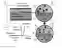
FIGS. 1A-1D are schematic illustrations of the ionic junction and radiation detector disclosed herein.
DESCRIPTION OF THE PREFERRED EMBODIMENT
We propose a transformative solution which would apply to all ionically bonded wide band gap semiconductors such as the thallium and lead halides and would lead to orders of magnitude decreased ionic currents as well as potentially improved electronic μτ products. We disclose a novel ionic “p-n” type junction in which the “p” region is, e.g. in TlBr, dominated by positively charged Br vacancies (VBr) and in which the “n” region is dominated by negatively charged. Tl vacancies (VTl) as shown in FIGS. 1A and 1B. In earlier studies, we already showed that Ph donors substituting on Tl sites are compensated by Tl vacancies and Se acceptors are compensated by Br vacancies. In a similar manner to a conventional junction, the ionic junction will form as the Tl (Br) vacancies diffuse respectively into the acceptor (donor) doped regions thereby annihilating each other and setting up depleted regions on both sides of the junction as well as a built-in electric field (ε) arising from the donor (DTl) and acceptor (ABr) dopants which are no longer compensated electrically by Tl and Br vacancies, respectively, as shown in FIG. 1C. Analogous to the traditional p-n junction where the number of electrons in the n-type region is equal to the number of donors and the number of electrons in the p-type region is equal to the equilibrium constant for electron-hole generation (the np product) divided by the acceptor concentration, the internal field or built-in voltage (Vbi) is given by
V bi = k T q ln ( [ V T l ′ ] n [ V T l ′ ] p ) = k T q ln ( N A N D K s ) ( 1 )
where the concentration of Tl vacancies in the n-type region, [VTl1]n, is equal to the donor concentration, ND, and the concentration of Tl vacancies in the p-type region, [VTl1]ρ, is given by the Schottky equilibrium constant, Ks, divided by the acceptor concentration, NA, k, T, and q are the Boltzmann constant, temperature, and elementary charge, respectively. For TlBr, Ks at room temperature is small relative to NAND and so a significant internal field can arise that acts as a voltage barrier (Vb) to defect migration with an effective depletion width in the material (W). Application of a bias (Va) modifies Vb as Vb=bi−Va so that when Va is positive, the barrier is reduced and the material is forward biased resulting in a transport of charged defects as shown in FIG. 1D. However, reversing the bias increases the barrier and there is very little ion migration.
This design is not limited to a homojunction of n and p type doped TlBr but could be applied to any ionic conductor which can be appropriately doped such that one side of the junction is dominated by positively charged ionic defects and the other side by negatively charged ionic defects. Furthermore, this design is not limited only to homojunctions but could equally well be applied to a heterojunction between two different ionic conductors, for example, donor doped. TlBr and acceptor doped. TlCl. A potential advantage in utilizing a heterojunction is that the different crystal lattice parameters characteristic of the two materials which make up the junction may serve to impede dopant migration across the junction that may occur in highly biased ionic materials. Another potential advantage of the heterojunction is to, for example, select a donor doped material with a high relative barrier to Tl diffusion and an acceptor doped material with a high relative bather to Br diffusion which will further impede majority carrier migration.
Several key implications regarding improved performance follow. First, as in conventional p-n junctions, the reverse bias current drops orders of magnitude below that expected based on the bulk resistivity of the p and n regions. First, this should serve to reduce the ionic dark current leading to a) higher sensitivity and b) reduced degradation due to reduced ionic electro migration. The latter should serve to extend the effective operating lifetime of such devices by orders of magnitude. Second, the built in field, as in PIN diodes, will aid in separating the photo-generated electrons and holes (FIG. 1C) and improve their μτ products.
Example
Sample Preparation
High purity TlBr is used as a starting material although less pure source materials may be adequate. Donor dopants are added as metal bromides and acceptor dopants as thallium chalcogenides (the level of doping is discussed in the doping conditions section). The dopant and TlBr are loaded into a quartz ampoule inside a nitrogen filled glove box to limit the exposure to moisture and air. The loaded ampoule is baked under vacuum at a temperature of 150° C. for 3 hours to remove adsorbed gas and moisture from the surface of the sample and ampoule. Then, the ampoule is sealed under vacuum and placed in a Vertical Bridgman 2-zone furnace. The sample is heated to above the melting temperature in the upper zone and then lowered into the second zone at a temperature just below the melting temperature for large crystal formation. The resulting boule is sectioned into disks approximately 2 cm in diameter and 1 mm thick and lapped and polished. In another process, the TlBr is zone refined using a horizontal bed for several passes in a gas environment containing hydrogen bromide gas. During the latter pass(es) the dopant material is added to the seed end of the boule and refined throughout the boule. The material is then sectioned as previously described. This concludes the fabrication of either an acceptor or donor doped sample.
Next, the ionic junction is formed by one of several methods, similar to those used to form p-n junctions in semiconductor devices. This may include liquid phase epitaxy. For example, a donor doped sample is placed in contact with a melt of acceptor doped TlBr and the acceptor doped TlBr solidifies epitaxially on the cooler donor doped sample, forming the junction. Alternatively, a donor doped single crystal wafer is exposed to a vapor containing acceptor like species at elevated temperatures. These acceptor species adsorb and then diffuse into the wafer. The depth of the junction is controlled by the time and temperature of the procedure. Yet another approach involves depositing a thin layer of material containing the acceptor species onto the surface of the wafer by physical or chemical vapor deposition methods and then heating it up to a temperature at which the dopant diffuses into the crystal at the desired diffusivity. In addition, the nominally donor doped single crystal wafer is exposed to a vapor containing acceptor doped TlBr at elevated temperature. The acceptor doped TlBr vapor deposits onto the wafer as an epitaxial p-type layer, forming the junction. Again, the depth of the junction is controlled by the time and temperature of the procedure. A fourth option can be ion-implanting the acceptor impurity into the surface of the wafer followed by a high temperature annealing process to remove the implantation damage. The depth of the junction is controlled by the implantation accelerating voltage. Other methods used by the semiconductor industry to form semiconductor junctions could also be applied to the formation of ionic junctions. Electrodes may be prepared for example by evaporation of Cr and then Au on either face of the sample and electrical leads of Pd attached to the electrodes with carbon paste. Alternate methods for applying electrodes and different electrode materials would also be acceptable.
Doping Conditions
Analogous to a p-n semiconductor diode, the optimum doping conditions for the ionic n and p type regions requires minimization of the reverse bias current or charge flux (Jo) given by
J o = qK s [ ( D Tl L Tl N A ) + ( D Br L Br N D ) ] ( 2 )
where Di is the diffusivity of vacancy i and Li is diffusion length which is in part related to the lifetime of the vacancy before recombination with its oppositely charged vacancy. The left term in brackets is due to Tl motion and the right term is due to Br motion. We have previously measured and modeled the conductivity (σ) in TlBr given by
σ i = q 2 k T D i [ i ] ( 3 )
where q, D, and [i] are elementary charge, diffusivity, and concentration of defect i (Tl or Br vacancies). Through doping with known amounts of acceptors or donors, as controlled which allowed the calculation of D for Tl and Br. The result is DBr≈10,000 DTl at room temperature meaning that, in equation 2, if NA is 1 ppm, ND should be approximately 10,000 so that both Tl and Br motion contribute equally to the current. Our previous research found that the solubility of Se and S acceptors (NA) is low in TlBr (<1 ppm) and that the maximum solubility of Pb donor (ND) appears to be on the order of 100 ppm. In this example, we suggest doping with 1 ppm acceptor and 100 ppm donor which will result in a larger contribution to dark current by Br motion. However, present knowledge attributes long term degradation of TlBr radiation detectors to Tl motion, therefore this doping level is advantageous.
It is recognized that modifications and variations of the invention disclosed will be apparent to those of ordinary skill in the art and it is intended that all such modifications and variations be included within the scope of the appended claims.
Claims
What is claimed is:1. Ionic junction comprising:
An ionically bonded wide band gap material having a first region dominated by positively charged ionic defects in intimate contact with a second region dominated by negatively charged ionic defects forming depleted regions on both sides of the junction resulting in a built-in electric field.
2. The ionic junction of claim 1 in which the positively charged ionic defects are anion vacancies and the negatively charged ionic defects are cation vacancies.
3. The ionic junction of claim 2 wherein the material is TlBr.
4. The ionic junction of claim 3 wherein the first region is doped with an acceptor material.
5. The ionic junction of claim 4 wherein the acceptor material is a thallium chalcogenide.
6. The ionic junction of claim 3 wherein the second region is doped with a donor material.
7. The ionic junction of claim 6 wherein the donor material is lead bromide.
8. The ionic junction of claim 1 wherein the material is a lead halide.
9. The ionic junction of claim 1 in which the positively charged ionic defects are anion vacancies and the negatively charged ionic defects are anion interstitials.
10. The ionic junction of claim 9 wherein the material is CaF2.
11. The ionic junction of claim 2 wherein the first region is doped with an acceptor material.
12. The ionic junction of claim 2 wherein the second region is doped with a donor material.
13. The ionic junction of claim 8 wherein the acceptor material is an alkali halide.
14. The ionic junction of claim 8 wherein the donor material is an yttrium halide.
15. The ionic junction of claim 1 in which the positively charged ionic defects are cation interstitials and the negatively charged ionic defects are cation vacancies.
16. The ionic junction of claim 15 wherein the material is LiI.
17. The ionic junction of claim 16 wherein the acceptor material is Li2O.
18. The ionic junction of claim 16 wherein the donor material is MgI2.
19. Ionic junction comprising:
A first ionically bonded wide band gap semiconductor material dominated by positively charge ionic defects in intimate contact with a second ionically bonded wide band gap semi conductor material dominated by negatively charged ionic detects forming depleted regions on both sides of the junction resulting in a built-in electric field.
20. The ionic junction of claim 19, wherein the first material is acceptor doped TlCl and the second material is donor doped TlBr.
21. The ionic junction of claim 19, wherein the first material is acceptor doped TlI and the second material is donor doped TlBr.
22. Radiation detector comprising:
An ionic junction including an ionically bonded wide band gap material having a first region dominated by positively charged ionic defects in intimate contact with a second region dominated by negatively charged ionic defects forming depleted regions on both sides of the junction resulting in a built-in electric field; and
Circuit means for establishing a voltage across the junction whereby radiation impinging upon the junction will cause a current to flow in the circuit.
23. The radiation detector of claim 22 wherein the wide band gap material is TlBr.
24. The radiation detector of claim 23 wherein the first region is doped with an acceptor material.
25. The radiation detector of claim 24 wherein the acceptor material is a thallium chalcogenide.
26. The radiation detector of claim 23 wherein the second region is doped with a donor material.
27. The radiation detector of claim 26 wherein the donor material is lead bromide.
28. Method for making an ionic junction comprising:
Doping a wide band gap material with an acceptor material to create positively charged ionic defects;
Doping a wide band gap material with a donor material to create negatively charged ionic defects; and
Using liquid phase epitaxy to form a junction between acceptor-doped material and the donor-doped material.
29. Method for making an ionic junction comprising:
Doping a wide band gap material with a donor material to form a single crystal wafer; and
Exposing the wafer to a vapor containing acceptor species that adsorb onto and then diffuse into the wafer.
30. Method for making an ionic junction comprising:
Doping a wide band gap material with a donor material to form a single-crystal wafer;
Depositing a thin layer of material containing acceptor species onto a surface of the wafer; and
Heating the wafer to a temperature at which the acceptor species diffuses into the wafer at a desired diffusivity.
31. The method of claim 30 wherein the depositing step uses physical or chemical vapor deposition.
32. Method for making an ionic junction comprising:
Doping a wide band gap material with a donor material to form a single-crystal wafer;
Depositing a thin layer of material containing acceptor species onto a surface of the wafer.
33. The method of claim 32 wherein the depositing step uses physical or chemical vapor deposition.
34. Method for making an ionic junction comprising:
Doping a wide band gap material with a donor material to form a single crystal wafer;
ion-implanting acceptor species into a surface of the wafer; and
Annealing the wafer at a high temperature to remove implantation damage.
Images & Drawings included:


Sources:
- United States Patent and Trademark Office - verify current appl. status at the USPTO↗
Recent applications in this class:
- » 20250091895 2025-03-20
INDIUM OXIDE NANORODS, METHODS FOR PREPARING AND USING SAME - » 20240409429 2024-12-12
POWDER OF GALLIUM NITRIDE AND METHOD FOR PRODUCING THE SAME - » 20240158254 2024-05-16
POWDER FOR GROWING GALLIUM OXIDE SINGLE CRYSTAL AND METHOD OF MANUFACTURING THE SAME - » 20240140816 2024-05-02
GALLIA PARTICLES AND METHOD FOR PRODUCING GALLIA PARTICLES - » 20240092650 2024-03-21
Method for improving conductivity and blue light filtering efficiency of transparent conducting oxide (TCO) - » 20220098052 2022-03-31
Preparation method of indium oxide with stable morphology and application thereof - » 20210309535 2021-10-07
Compound - » 20210276879 2021-09-09
Method of preparing indium oxide spherical powder - » 20160326008 2016-11-10
INDIUM-CONTAINING FILM AND COMPOSITION FOR FORMING THE SAME - » 20160297686 2016-10-13
Oxide semiconductor
Recent applications for this Assignee:
- » 20250288624 2025-09-18
LONG-TERM STABILIZATION, FORMULATION AND TABLETING OF LIVE MICROBIAL CELLS - » 20250284856 2025-09-11
GENERALIZABLE END-TO-END AUTONOMOUS DRIVING WITH MULTI-MODAL FOUNDATION MODELS - » 20250283816 2025-09-11
COMPOSITIONS FOR DETECTION OF FLUOROCARBONS AND RELATED ARTICLES, SYSTEMS, AND METHODS - » 20250281931 2025-09-11
High-Throughput Expansion Microscopy, Devices for Use With a Well Plate and Methods for Processing a Sample - » 20250278625 2025-09-04
VISUOMOTOR POLICY LEARNING VIA ACTION DIFFUSION - » 20250275716 2025-09-04
SENSORIZED WEARABLE GARMENT - » 20250275026 2025-08-28
ELECTRICALLY CONDUCTIVE FIREBRICK SYSTEM - » 20250263824 2025-08-21
ADDITIVELY MANUFACTURED OXIDE DISPERSION-STRENGTHENED ALLOY - » 20250261881 2025-08-21
FLEXIBLE ELECTRONICS FOR ANALYTE DETECTION - » 20250257316 2025-08-14
CONTROL OF NITROGEN FIXATION IN RHIZOBIA THAT ASSOCIATE WITH CEREALS