INTEGRATED OPTICAL DEVICE INCLUDING SUBSTRATES STACKED ALONG AN OPTICAL AXIS THEREOF
US20120155798A1
2012-06-21
13/285,706
2011-10-31
Abstract:
An optical device includes a first substrate having a first top surface and a first bottom surface, a second substrate having a second top surface and a second bottom surface, and a spacer substrate between substantially planar portions of the second top surface and the first bottom surface. The spacer, first, and second substrates seal an interior space between the second top surface of the second substrate and the first bottom surface of the first substrate. At least two of the first, second, and spacer substrates are aligned and secured on a wafer level. An optoelectronic element is within the interior space. An optical axis of the optical device extends through one of the first top and bottom surfaces and the second top and bottom surfaces. An electrical interconnection extends from the optoelectronic element to outside the interior space.
Inventors:
- Michael R. FELDMAN 56 🇺🇸 Huntersville, NC, United States
- James E. MORRIS 46 🇺🇸 Lake Wylie, SC, United States
Interested in similar patents?
Get notified when new applications in this technology area are published.
Classification:
G01J1/02 » CPC main
Photometry, e.g. photographic exposure meter Details
G01J1/0204 » CPC further
Photometry, e.g. photographic exposure meter; Details Compact construction
G01J1/0271 » CPC further
Photometry, e.g. photographic exposure meter; Details Housings; Attachments or accessories for photometers
G02B6/4246 » CPC further
Light guides; Coupling light guides; Coupling light guides with opto-electronic elements; Packages, e.g. shape, construction, internal or external details Bidirectionally operating package structures
G02B6/4292 » CPC further
Light guides; Coupling light guides; Coupling light guides with opto-electronic elements the light guide being disconnectable from the opto-electronic element, e.g. mutually self aligning arrangements
G01J1/0403 » CPC further
Photometry, e.g. photographic exposure meter; Details; Optical or mechanical part supplementary adjustable parts Mechanical elements; Supports for optical elements; Scanning arrangements
G02B6/4249 » CPC further
Light guides; Coupling light guides; Coupling light guides with opto-electronic elements; Packages, e.g. shape, construction, internal or external details comprising arrays of active devices and fibres
G02B6/12 IPC
Light guides of the optical waveguide type of the integrated circuit kind
Description
CROSS REFERENCE TO RELATED APPLICATIONS
This application is a continuation of application Ser. No. 12/801,941, filed Jul. 2, 2010, which is a continuation of Ser. No. 12/379,279, filed Feb. 18, 2009, now Pat. No. 7,750,289 B2, which is a continuation of Ser. No. 11/651,525, filed Jan. 10, 2007, abandoned, which in turn is a continuation of Ser. No. 11/127,284, filed May 12, 2005, now Pat. No. 7,375,315 B2, which is a continuation of Ser. No. 10/231,483, filed Aug. 30, 2002, abandoned, which is a continuation of PCT/US01/07053, filed Mar. 6, 2001, which claims priority to provisional application Ser. No. 60/187,034, filed Mar. 6, 2000, and is a continuation-in-part of U.S. patent application Ser. No. 09/418,022 filed Oct. 14, 1999, now Pat. No. 6,374,004, entitled “Optical Subassembly,” and a continuation-in-part of U.S. patent application Ser. No. 09/418,365 filed Oct. 14, 1999, now Pat. No. 6,406,195, entitled “Interface Between Opto-electronic Devices and Fibers,” the entire contents of all of which are hereby incorporated by reference in their entirety for all purposes.
BACKGROUND OF THE INVENTION
Previous attempts at integrating a transceiver on a chip involved using monolithic integration, in which the active elements are formed in the substrate, and are thus all made of the same material. This does not allow optimum performance to be realized for at least one of the detector array and the light source array.
Other attempts have placed the active elements, e.g., the light sources and the detectors, on different substrates. However, this increases the complexity of the system due to an increased number of components and alignment difficulty.
SUMMARY OF THE INVENTION
One or more embodiments are directed to an optical device including a first substrate having a first top surface and a first bottom surface, a second substrate having a second top surface and a second bottom surface, a spacer substrate between a substantially planar portion of the second top surface of the second substrate and a substantially planar portion of the first bottom surface of the first substrate, the spacer substrate, the first substrate and the second substrate sealing an interior space between the second top surface of the second substrate and the first bottom surface of the first substrate, at least two of the first substrate, the second substrate, and the spacer substrate being aligned and secured on a wafer level, an optoelectronic element within the interior space, an optical axis of the optical device extending through one of the first top and bottom surfaces and the second top and bottom surfaces, and an electrical interconnection extending from the optoelectronic element to outside the interior space.
The optoelectronic element may transmit light.
The optical device may be used in a laser pointer.
The optical device may be used with a plurality of fibers.
The optoelectronic element may detect light and output an electrical signal in response thereto.
The optical device may be used with a plurality of fibers.
The optoelectronic element may be a transceiver.
The optical device may be used in an optical head.
The optical device may be used in a data storage system.
BRIEF DESCRIPTION OF THE DRAWINGS
Features will become apparent to those of ordinary skill in the art by describing in detail exemplary embodiments with reference to the attached drawings, in which:
FIG. 1 is an elevational exploded top view of an optical transceiver according to an embodiment;
FIG. 2 is an elevational side view of another optical transceiver according to an embodiment;
FIG. 3 is a top view of another configuration of the light sources and detectors on the same substrate;
FIG. 4 is a schematic side view of the creation of multiple transceivers according to an embodiment; and
FIG. 5 is an exploded elevational perspective view of an interface in conjunction with fibers in a housing and the transceiver according to an embodiment.
DETAILED DESCRIPTION OF THE INVENTION
In the following description, for purposes of explanation and not limitation, specific details are set forth in order to provide a thorough understanding of the present invention. However, it will be apparent to one skilled in the art that the present invention may be practiced in other embodiments that depart from these specific details. In other instances, detailed descriptions of well-known devices and methods are omitted so as not to obscure the description of the present invention with unnecessary details.
Rather than using monolithic integration, many of the advantages of integration can still be realized by providing the light source array and the detector array on the same surface of a single substrate and providing an optics block having the optical elements for both the light source array and the detector array integrated therein.
Related, co-pending U.S. Provisional Application Ser. No. 09/690,763 entitled “Fiber Interfaces Including Parallel Arrays, Power Monitoring and/or Differential Mode Delay Compensation” filed on Oct. 18, 2000, describes a laser array and a detector array on the same substrate. In this previous application, the detector array was used for monitoring the power of the lasers, a portion of the output laser beams being directed to the detector. In accordance with the present disclosure, a light source array and a detector array are integrated on the same substrate, but, as shown in FIGS. 1 and 2 of the present application, these detectors are for receiving a signal from a remote location, not for monitoring the light source array. Of course, an additional array of monitor detectors could be provided for monitoring the output of the light sources.
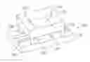
In FIG. 1, an optical transceiver 100 includes a light source array 102, here shown as a vertical cavity side emitting laser (VCSEL) array, and a detector array 104 are integrated on a silicon wafer 106. Silicon interconnect tracks 108 supply power to the active elements 102, 106 and pads 110 allow the detector signals to be read out.
An optics block 120 contains two sets of integrated optics, one set 122 for the light source array 102 and one set 124 for the detector array 104. The integrated optics 122 for the light source receive light from the light source array 102 and direct the light to a desired application. The integrated optics 124 for the detectors receive light from a desired application and direct the light to the detector array 104. The optics may be diffractives, refractives or hybrids thereof and may be formed lithographically on the optics block 120.
The integrated optics 122, 124 for the light source array and the detector array may include optical elements formed on either or both surfaces of the optics block 120. Since the optics for both the light source array and the detector array are aligned simultaneously, the assembly and alignment steps required for creating a transceiver are reduced. Further, the integration allows the transceiver to be smaller and have fewer parts. Depending upon the material used for the substrate, either the detector array or the light source array may be monolithically integrated therein.
The transceiver 100 also includes a spacer 130 between the active elements and the optics block 120. The spacer may be an integrated spacer surrounding the perimeter of the optics block, as shown in FIG. 1. The spacer may be a separate element, formed in the optics block or formed in the substrate. The spacer may serve to protect the active elements.
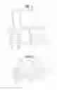
In FIG. 2, the bonded structure of a transceiver 200 is shown. Rather than having a spacer 130 around the perimeter of the optics block 120, separate spacer elements 230 are positioned at the corners of the optics block. Also, the optics 222 for the light sources 202 are on a different surface of the optics block 220 than the optics 224 for the detectors 204. The optics for both the light sources and the detectors may have the same design. Again, light sources 202 and detectors 204 are on the same substrate 206, and one of them may be monolithically integrated therein. Silicon tracks 208 and pads 208 for providing power and signals to and from the active elements are also on the substrate.
FIG. 3 is a top view of a transceiver 300 in accordance with another embodiment of the present invention. In FIG. 3, rather than having the active elements 102, 104 arranged in parallel arrays, the active elements form a linear array. In the particular example shown in FIG. 3, four light sources 102 and four detectors 104 are in a line. The spacing therebetween reduces cross-talk between the active devices. Corresponding optical elements 122,124 are also now in a single line. This configuration allows a standard 1 x 12 fiber array to be connected with the transceiver. This configuration also allows all the required interconnection to be provided on a same side of the substrate 106, thereby allowing the optics block 120 and the substrate 106 to share a common edge, which may facilitate manufacturing at the wafer level.
In any of the configurations, the components may be attached using wafer-to-wafer bonding techniques, as set forth, for example, in U.S. Pat. Nos. 6,096,155 and 6,104,690, commonly assigned, which are hereby incorporated by reference in their entirety for all purposes. Both of the above configurations allow the optics for both the transmitter portion and the receiver portion to be aligned simultaneously. As used herein, the term wafer is meant to generally refer to any structure having more than one component which is to be singulated, e.g., diced, for final use. The resultant wafer having a plurality of the transceivers thereon is then singulated, i.e., vertically separated, to form a plurality of transceivers.
A particular example of wafer bonding all three substrates together before separating is shown in FIG. 4. By creating spaces 340 between the sets of optical elements 122, 124 for each transceiver and spaces 342 between the spacers 130 for each transceiver, e.g., by etching in silicon as shown, the individual transceivers may be realized by separating the substrate 106 containing the light sources 102 and detectors 304 at the appropriate points. As shown in FIG. 4, the detectors 304 are monolithically integrated into the substrate 106. Whichever active element to be provided on the substrate has the higher effective yield is preferably the monolithically integrated element, since the monolithically integrated elements will not be able to be substituted out. Further, the metalization required for the electrical connections for both the monolithically integrated element and the additional active element on the substrate are formed using the same mask set as that for forming the monolithically integrated element. This helps insure precise alignment, since the active element to be mounted can use its metalization to provide its alignment, e.g., by solder self-alignment. The active elements that are to be mounted on the substrate may then be tested before being mounted. After mounting, they may be tested again and replaced if required before the wafer bonding. As used herein, bonding may include any type of attachment, including the use of bonding materials, surface tension or directly forming on the same substrate. As used herein, separating or singulating may include any means for realizing individual components, e.g., dicing.
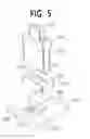
The alignment of the active elements to the input and output ports corresponding thereto, typically fibers, is particularly important. One configuration for insuring proper alignment between the transceiver and fibers is shown in FIG. 5. As can be seen in FIG. 5, a plurality of fibers 410 are inserted into a ferrule 412. The active elements of the present invention, here the linear configuration as shown in FIG. 3, which are to be in communication with the fibers 410, are preferably provided on a silicon bench or sub-mount 416, corresponding to the common substrate 106 in FIG. 3. In turn, this silicon bench 416 is preferably provided on a substrate 418. An optics block 420 provides at least one optical element between each opto-electronic device on the sub-mount 416 and a corresponding fiber 410. The optics block 420 is preferably spaced from the opto-electronic devices by a spacer 415. The optical elements preferably include elements which collimate, focus, homogenize or otherwise couple the light. Since the optics block has two surfaces, two optical elements may be provided thereon. Further, if required, additional optics blocks may be bonded to and spaced from the optics block 420 to provide additional surfaces, as with any of the previous transceiver configurations.
The spacer 415 is then bonded, e.g., using solder or epoxy, into place on the bench 416. The bevels which can be seen on the interior surface of the spacer 415 simply arise when using silicon as the spacer and the hole therein is formed by wet etching silicon along its crystalline plane. While wet-etching is a simple way of forming the hole in the spacer, vertical side walls may be more advantageous, e.g., for load bearing. Substantially vertical side walls may be realized by dry etching silicon. Further, other materials such as ceramic, glass, plastic, may be used for the spacer 415. If the spacer 415 is transparent to wavelengths of interest, the hole therein may not be required.
Preferably, the alignment and bonding of the spacer 415 and the optics block 420 occur on a wafer level, and then diced to form respective dies which are then aligned to the bench 416. The alignment of the spacer 415 is not very sensitive, i.e., the spacer just needs to be aligned so that it does not block light between the optics block 420 and the opto-electronic device. While a spacer 415 may be formed directly on the optics block 420 itself, the use of a separate spacer 15 allows larger vertical separation to be achieved. The use of a separate spacer is particularly advantageous when providing optical elements on a bottom surface of the optics block 20, since the processes for forming the optics and the spacer features interfere with each other. Finally, use of a separate spacer allows the sealing off of the opto-electronic device to be more readily and stably achieved. Such sealing protects the opto-electronic device from environmental factors, such as humidity.
A mechanical interface 422 aligns the optics block 420, which is already aligned with the electro-optical devices, with the fibers 410. This may be achieved by the provision of alignment features on both the mechanical interface 422 and the ferrule 412 housing the fibers 410. In the particular example shown, these alignment features consist of holes 424 in the ferrule 412, which are already typically present for aligning the ferrule with other devices, and alignment holes 426 in the mechanical interface 422. Once these alignment holes 424, 426 are aligned, an alignment pin, not shown, may then be inserted therein to maintain the aligned position. Further details of such interfaces may be found, for example, in commonly assigned, co-pending application U.S. Ser. No. 09/418,022, now U.S. Pat. No. 6,374,004, entitled “Optical Subassembly” which is incorporated by reference in its entirety for all purposes.
While the present invention is described herein with reference to illustrative embodiments for particular applications, it should be understood that the present invention is not limited thereto. Those having ordinary skill in the art and access to the teachings provided herein will recognize additional modifications, applications, and embodiments within the scope thereof and additional fields in which the invention would be of significant utility without undue experimentation. Thus, the scope of the invention should be determined by the appended claims and their legal equivalents, rather than by the examples given.
Claims
What is claimed is:1. An optical device, comprising:
a first substrate having a first top surface and a first bottom surface;
a second substrate having a second top surface and a second bottom surface;
a spacer substrate between a substantially planar portion of the second top surface of the second substrate and a substantially planar portion of the first bottom surface of the first substrate, the spacer substrate, the first substrate and the second substrate sealing an interior space between the second top surface of the second substrate and the first bottom surface of the first substrate, at least two of the first substrate, the second substrate, and the spacer substrate being aligned and secured on a wafer level;
an optoelectronic element within the interior space, an optical axis of the optical device extending through one of the first top and bottom surfaces and the second top and bottom surfaces; and
an electrical interconnection extending from the optoelectronic element to outside the interior space.
2. The optical device as claimed in claim 1, wherein the optoelectronic element transmits light.
3. The optical device as claimed in claim 2, wherein the optical device is used in a laser pointer.
4. The optical device as claimed in claim 2, wherein the optical device is used with a plurality of fibers.
5. The optical device as claimed in claim 1, wherein the optoelectronic element receives light.
6. The optical device as claimed in claim 5, wherein the optical device is used with a plurality of fibers.
7. The optical device as claimed in claim 1, wherein the optoelectronic element is a transceiver.
8. The optical device as claimed in claim 1, wherein the optical device is used in an optical head.
9. The optical device as claimed in claim 1, wherein the optical device is used in data storage.
Images & Drawings included:
Sources:
- United States Patent and Trademark Office - verify current appl. status at the USPTO↗
Recent applications in this class:
- » 20250155279 2025-05-15
NANOCATENANE STRUCTURE AND NANOMACHINE INCLUDING NANOCATENANE STRUCTURE - » 20240151577 2024-05-09
Control system for an active shielding screen - » 20240125643 2024-04-18
Wireless battery-powered daylight sensor - » 20220155140 2022-05-19
Wireless battery-powered daylight sensor - » 20190137331 2019-05-09
Imaging apparatus with infrared-based temperature detection devices - » 20180364094 2018-12-20
Terahertz detection sensor and terahertz image measurement device - » 20180259386 2018-09-13
Environmental sensor - » 20180031415 2018-02-01
INTERFEROMETER SYSTEM HAVING A CONTINUOUSLY VARIABLE BROADBAND REFLECTOR AND METHOD TO GENERATE AN INTERFERENCE SIGNAL OF A SURFACE OF A SAMPLE - » 20160025553 2016-01-28
METHOD FOR WIRELESS SIGNAL TRANSMISSION AND SENSOR-CONTROLLED COMPONENT - » 20140374569 2014-12-25
Frequency visualization apparatus and method