METHOD FOR FABRICATING LIGHT EMITTING DIODE CHIP
US20120156815A1
2012-06-21
13/207,441
2011-08-11
Abstract:
A method for fabricating an LED chip includes: providing a sapphire substrate with a SiO2 pattern layer formed on the substrate; forming a lighting structure on the sapphire substrate with the SiO2 pattern layer; forming grooves in the lighting structure to divide the lighting structure into a number of light emitting regions, the grooves extending to the sapphire substrate and revealing the SiO2 pattern layer; removing the SiO2 pattern layer and forming spaces between the lighting structure and the substrate; etching part of the light emitting regions, and then forming electrodes on the light emitting regions; and cutting the sapphire substrate along the grooves to obtain a plurality of LED chips.
Assignee:
- ADVANCED OPTOELECTRONIC TECHNOLOGY, INC. 420 🇹🇼 Hsinchu Hsien, Taiwan
Interested in similar patents?
Get notified when new applications in this technology area are published.
Classification:
H01L33/007 » CPC main
Semiconductor devices with at least one potential-jump barrier or surface barrier specially adapted for light emission; Processes or apparatus specially adapted for the manufacture or treatment thereof or of parts thereof; Details thereof; Processes for devices with an active region comprising only III-V compounds with a substrate not being a III-V compound comprising nitride compounds
H01L33/0095 » CPC further
Semiconductor devices with at least one potential-jump barrier or surface barrier specially adapted for light emission; Processes or apparatus specially adapted for the manufacture or treatment thereof or of parts thereof; Details thereof; Processes Post-treatment of devices, e.g. annealing, recrystallisation or short-circuit elimination
H01L33/20 » CPC further
Semiconductor devices with at least one potential-jump barrier or surface barrier specially adapted for light emission; Processes or apparatus specially adapted for the manufacture or treatment thereof or of parts thereof; Details thereof characterised by the semiconductor bodies with a particular shape, e.g. curved or truncated substrate
H01L21/78 IPC
Processes or apparatus adapted for the manufacture or treatment of semiconductor or solid state devices or of parts thereof; Manufacture or treatment of devices consisting of a plurality of solid state components formed in or on a common substrate or of parts thereof; Manufacture of integrated circuit devices or of parts thereof; Manufacture or treatment of devices consisting of a plurality of solid state components or integrated circuits formed in, or on, a common substrate with subsequent division of the substrate into plural individual devices
Description
TECHNICAL FIELD
The disclosure generally relates to methods for fabricating light emitting diode chips, and particularly to a method for fabricating light emitting diodes with high lighting efficiency.
DESCRIPTION OF RELATED ART
In recent years, due to excellent light quality and high luminous efficiency, light emitting diodes (LEDs) have increasingly been used as substitutes for incandescent bulbs, compact fluorescent lamps and fluorescent tubes as a light source of illumination devices.
A conventional LED includes a substrate and a light emitting structure formed on the substrate. However, the light from the light emitting structure will be absorbed by the substrate and converted into thermal energy when travels to the substrate, therefore decreasing the lighting efficiency of the light emitting structure.
Therefore, a method for fabricating an LED chip is desired to overcome the above described shortcomings.
BRIEF DESCRIPTION OF THE DRAWINGS
Many aspects of the disclosure can be better understood with reference to the following drawings. The components in the drawings are not necessarily drawn to scale, the emphasis instead being placed upon clearly illustrating the principles of the disclosure. Moreover, in the drawings, like reference numerals designate corresponding parts throughout the several views.
FIG. 1-FIG. 9 are diagrams schematically showing the process of a method for fabricating an LED chip according to a first embodiment of the present disclosure.
FIG. 10 is an illustrating view of a sapphire substrate according to a second embodiment of the present disclosure.
DETAILED DESCRIPTION
An embodiment for fabricating an LED chip will now be described in detail below and with reference to the drawings.
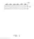
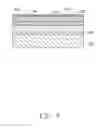
Referring to FIG. 1, a sapphire substrate 110 is provided, and then a SiO2 pattern layer 120 is formed on the sapphire substrate 110. Further referring to FIG. 2, the SiO2 pattern layer 120 includes a number of SiO2 strips paralleled to each other. Referring also to FIG. 3, a cross section of the SiO2 strips is trapezoid-shaped. In an alternative embodiment, the cross section of the SiO2 strips can be semicircle-shaped.
Referring to FIG. 3, a light emitting structure 130 is formed on an outer surface of the sapphire substrate 110 with the SiO2 pattern layer 120, by metal organic chemical vapor deposition (MOCVD) or molecular beam epitaxy (MBE). The light emitting structure 130 includes a n-type GaN layer 131, a multiple quantum well (MQW) layer 132 and a p-type GaN layer 133 formed subsequently in a direction away from the sapphire substrate 110.
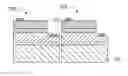
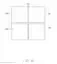
Referring to FIG. 4, grooves 140 are formed on the lighting structure 130 by dry etching to divide the lighting structure 130 into a number of light emitting regions 150. The grooves 140 extend from an upper surface of the lighting structure 130 to the sapphire substrate 110 and reveal part of the SiO2 pattern layer 120. In this embodiment, two grooves 140 intersect each other and divide the lighting structure 130 into four light emitting regions 150, as shown in FIG. 5.
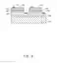
Referring to FIG. 6, the SiO2 pattern layer 120 is removed by using a buffered oxide etch (BOE) solution. The BOE solution is a mixture of hydrofluoric acid (HF) and ammonium fluoride (NH4F). The BOE solution can effectively etch the SiO2 pattern layer 120 when permeating into the grooves 140. After the SiO2 pattern layer 120 is removed, through holes 160 are formed between the lighting structure 130 and the sapphire substrate 110.
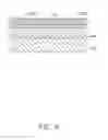
Referring to FIG. 7, after the etching of the SiO2 pattern layer 120 is finished, an indium-tin oxide (ITO) transparent conductive layer 134 is formed on a surface of the light emitting regions 150. The ITO transparent conductive layer 134 can improve the current diffusion on the surface of the light emitting regions 150.
Referring to FIG. 8, part of the light emitting regions 150 are etched to expose part surface of the n-type GaN layer 131 as an electrode supporting platform 170. A p-type electrode 171 and an n-type electrode 172 are then formed on the p-type GaN layer 133 and the electrode supporting platform 170 (i.e. the exposed surface of the n-type GaN layer 131), respectively. The p-type electrode 171 and the n-type electrode 172 can be formed by vacuum evaporation or sputtering. Materials of the p-type electrode 171 and the n-type electrode 172 can be selected from a group consisting of Ti, Al, Ag, Ni, W, Cu, Pd, Cr, Au and alloy thereof.
Referring to FIG. 9, the sapphire substrate 110 is cut along the grooves 140 by laser cutting or mechanical cutting and a number of LED chips 110 are obtained.
When a voltage is applied between the p-type electrode 171 and the n-type electrode 172, hole-electron capture will happen at the MQW layer 132, and energy is released in the form of light. When the light from the MQW layer 132 travels to the sapphire substrate 110, the light will be totally reflected back by inclined sidewalls of the through holes 160 and successively travels to outer environment through the p-type GaN layer 133. That is, the through holes 160 between the lighting structure 130 and the sapphire substrate 110 can reduce light being absorbed by the sapphire substrate 110, and improve the lighting efficiency of the LED chip 100.
The SiO2 pattern layer is not limited to the SiO2 strips parallel to each other. Referring to FIG. 10, a SiO2 pattern layer 220 in accordance with a second embodiment is formed on a surface of a sapphire substrate 210. The SiO2 pattern layer 220 includes SiO2 blocks arranged as a grid structure. The sapphire substrate 210 and the SiO2 pattern layer 220 can replace the sapphire substrate 110 and the SiO2 pattern layer 120 in the first embodiment.
It is believed that the present embodiments and their advantages will be understood from the foregoing description, and it will be apparent that various changes may be made thereto without departing from the spirit and scope of the disclosure or sacrificing all of its material advantages, the examples hereinbefore described merely being preferred or exemplary embodiments of the disclosure.
Claims
What is claimed is:1. A method for fabricating an LED chip, comprising:
providing a sapphire substrate with a SiO2 pattern layer formed on the substrate;
forming a lighting structure on the sapphire substrate with the SiO2 pattern layer;
forming grooves in the lighting structure to divide the lighting structure into a number of light emitting regions, the grooves extending to the sapphire substrate and revealing the SiO2 pattern layer;
removing the SiO2 pattern layer and forming spaces between the lighting structure and the substrate;
etching part of the light emitting regions, and then forming electrodes on the light emitting regions; and
cutting the sapphire substrate along the grooves to obtain a plurality of LED chips.
2. The method for fabricating an LED chip of claim 1, wherein the SiO2 pattern layer comprises a plurality of SiO2 strips paralleled to each other.
3. The method for fabricating an LED chip of claim 1, wherein the SiO2 pattern layer comprises a plurality of SiO2 blocks arranged as a grid structure.
4. The method for fabricating an LED chip of claim 2, wherein the cross sections of the SiO2 strips along the length direction of the strips are trapezoid-shaped.
5. The method for fabricating an LED chip of claim 1, wherein the SiO2 pattern layer is removed by BOE solution.
6. The method for fabricating an LED chip of claim 5, wherein the BOE solution is a mixture of hydrofluoric acid (HF) and ammonium fluoride (NH4F).
7. The method for fabricating an LED chip of claim 1, wherein the light emitting structure comprises an n-type GaN layer, a MQW layer and a p-type GaN layer formed subsequently in a direction away from the sapphire substrate.
8. The method for fabricating an LED chip of claim 7, wherein an ITO transparent conductive layer is further formed on the p-type GaN layer before etching part of the light emitting regions.
9. The method for fabricating an LED chip of claim 7, wherein part of the lighting regions are etched to expose part of the n-type GaN layer as an electrode supporting platform, and then a p-type GaN electrode and an n-type GaN electrode are formed on the p-type GaN layer and the exposed n-type GaN layer respectively.
10. The method for fabricating an LED chip of claim 1, wherein material of the electrode is selected from a group consisting of Ti, Al, Ag, Ni, W, Cu, Pd, Cr, Au and alloy thereof.
11. The method for fabricating an LED chip of claim 1, wherein the grooves are formed in the lighting structure by dry etching.
Images & Drawings included:


Sources:
- United States Patent and Trademark Office - verify current appl. status at the USPTO↗
Similar patent applications:
- » 20140151633
Light emitting diode chip having wavelength converting layer and method of fabricating the same, and package having the light emitting diode chip and method of fabricating the same - » 20110284822
Light emitting diode chip having wavelength converting layer and method of fabricating the same, and package having the light emitting diode chip and method of fabricating the same - » 20180006198
Light emitting diode chip having wavelength converting layer and method of fabricating the same, and package having the light emitting diode chip and method of fabricating the same - » 20160351759
Light emitting diode chip having wavelength converting layer and method of fabricating the same, and package having the light emitting diode chip and method of fabricating the same - » 20100167434
Method for fabricating light emitting diode chip - » 20110318855
Method for fabricating light emitting diode chip - » 20100041173
Method of fabricating light emitting diode chip - » 20050017259
Chip light emitting diode and fabrication method thereof - » 20110045622
Fabricating method of light emitting diode chip - » 20100252845
White-light light emitting diode chips and fabrication methods thereof
Recent applications in this class:
- » 20250015224 2025-01-09
Process for manufacturing an electroluminescent device - » 20240429343 2024-12-26
Method for monolithic integration preparation of full-color nitride semiconductor micro light-emitting diode array - » 20240421246 2024-12-19
LIGHT EMITTING DIODE CONTAINING PINHOLE MASKING LAYER AND METHOD OF MAKING THEREOF - » 20240313148 2024-09-19
METHOD FOR PRODUCING A RADIATION-EMITTING SEMICONDUCTOR CHIP AND RADIATION-EMITTING SEMICONDUCTOR CHIP - » 20240297266 2024-09-05
METHOD OF MANUFACTURING ALUMINUM NITRIDE LAYER - » 20240282883 2024-08-22
METHOD FOR MANUFACTUING NON-EMITTING III-NITRIDE SEMICONDUCTOR STACKED STRUCTURE - » 20240266462 2024-08-08
LASER ETCHING FOR LIGHT-EMITTING DIODE DEVICES AND RELATED METHODS - » 20240243219 2024-07-18
AIN Layer, Its Fabrication Process and Epitaxial Wafer - » 20240222546 2024-07-04
MANUFACTURING METHOD FOR HIGH-VOLTAGE LED CHIP - » 20240194822 2024-06-13
FABRICATION METHOD FOR SMALL SIZE LIGHT EMITING DIODES ON HIGH-QUALITY EPITAXIAL CRYSTAL LAYERS
Recent applications for this Assignee:
- » 20220252938 2022-08-11
Light emitting diode device, backlight module, and liquid crystal display device having same - » 20220077345 2022-03-10
Back plate and method for fluid-assisted assembly of micro-LEDs thereon - » 20210359153 2021-11-18
Back plate and method for fluid-assisted assembly of micro-LEDs thereon - » 20200326594 2020-10-15
Optical lens, backlight module and display device using same - » 20190326489 2019-10-24
Light emitting diode package - » 20190319173 2019-10-17
Side-view light emitting diode package structure - » 20190140136 2019-05-09
Manufacturing method for light emitting diode crystal grains using adhesive layer on auxiliary substrate to fill gaps between light emitting diode crystal grains - » 20190103512 2019-04-04
Light emitting diode structure - » 20190033659 2019-01-31
Liquid crystal display device - » 20180212105 2018-07-26
Flip chip light emitting diode and method of manufacturing the same