Fixed dead time PFC controller
US20120299570A1
2012-11-29
13/118,208
2011-05-27
✅ Patent granted
US 8,390,357 B2
2013-03-05
-
-
An Luu
Shimokaji & Associates P.C.
2031-10-20
Abstract:
A fixed dead time PFC controller, comprising: an amplitude normalization circuit, used to generate a normalized signal according to a full-wave rectified input voltage; a comparator circuit, used to compare the normalized signal with a threshold voltage to generate a select signal, wherein the select signal exhibits a first state when the normalized signal is higher than the threshold voltage, and a second state when the normalized signal is lower than the threshold voltage; and a driving signal selection circuit, having a first input end coupled to a first driving signal, a second input end coupled to a second driving signal, a control end coupled to the select signal, and an output end for outputting a gate driving signal.
Inventors:
- Yen-Hui Wang 3 🇹🇼 Taipei City, Taiwan
- Chia-Chieh Hung 2 🇹🇼 Taipei City, Taiwan
- Chia-Chieh HUNG 5 🇹🇼 Taipei, Taiwan
- Yen-Hui WANG 7 🇹🇼 Taipei, Taiwan
Assignee:
- Immense Advance Technology Corp. 4 🇹🇼 Neihu District, Taipei, Taiwan
Applicant:
Interested in similar patents?
Get notified when new applications in this technology area are published.
Classification:
H02M1/4208 » CPC main
Details of apparatus for conversion; Circuits or arrangements for compensating for or adjusting power factor in converters or inverters Arrangements for improving power factor of AC input
Y02B70/10 » CPC further
Technologies for an efficient end-user side electric power management and consumption Technologies improving the efficiency by using switched-mode power supplies [SMPS], i.e. efficient power electronics conversion e.g. power factor correction or reduction of losses in power supplies or efficient standby modes
Y02P80/10 » CPC further
Climate change mitigation technologies for sector-wide applications Efficient use of energy, e.g. using compressed air or pressurized fluid as energy carrier
Y02P80/10 » CPC further
Climate change mitigation technologies for sector-wide applications Efficient use of energy, e.g. using compressed air or pressurized fluid as energy carrier
G05F1/618 IPC
Automatic systems in which deviations of an electric quantity from one or more predetermined values are detected at the output of the system and fed back to a device within the system to restore the detected quantity to its predetermined value or values, i.e. retroactive systems; Regulating voltage or current wherein the variable actually regulated by the final control device is dc using semiconductor devices in series and in parallel with the load as final control devices
G06F1/04 IPC
Details not covered by groups - and Generating or distributing clock signals or signals derived directly therefrom
Description
BACKGROUND OF THE INVENTION
1. Field of the Invention
The present invention relates to a power conversion controller, and more particularly to a power conversion controller capable of providing PFC (Power Factor Correction) for power conversion applications.
2. Description of the Related Art
FIG. 1 illustrates a power conversion application, in which a prior art PWM/PFC circuit capable of providing a PWM (Pulse Width Modulation) function and a power factor correction function is used to control a BUCK conversion such that the waveform of an input current of the BUCK power conversion application is analog to that of a full-wave rectified input voltage VFull—Wave, and a regulated DC output voltage VO (or output current IO) is generated. As can be seen in FIG. 1, the power conversion application includes a PWM/PFC circuit 100, a power switch 101, a diode 102, an inductor 103, and a load 104.
The PWM/PFC circuit 100 is used to generate a driving signal VG according to a feedback signal VFB and the full-wave rectified input voltage VFull—Wave, so that the output voltage VO or output current IO is regulated at a DC value with the input current IIN following the full-wave rectified input voltage VFull—Wave, wherein the feedback signal VFB is generally derived from the output voltage VO or from the input current IIN.
The power switch 101, typically a MOSFET, is used to control the power conversion from the full-wave rectified input voltage VFull—Wave to the output voltage VO.
The diode 102 is used as a unilateral switch to release the energy stored in the inductor 103 when the power switch 101 is turned off.
The inductor 103 is used to store energy in the form of current when the power switch is turned on, and release the stored energy to the load 104 when the power switch 101 is turned off.
The load 104 can be a resistive load or a non-resistive load composed of LEDs.
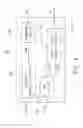
When in operation, due to the full-wave rectified waveform, the voltage level of VFull—Wave falls below the output voltage VO during part of a period, and no energy is transformed from VFull—Wave to VO during that part of a period. As a result, the energy delivered to the load 104 in a period is dependent on the amplitude of VFull—Wave, the higher the amplitude, the more energy delivered in a period. Please refer to FIG. 2, which illustrates the waveforms of a high amplitude full-wave rectified input voltage VFull—Wave.High and a low amplitude full-wave rectified input voltage VFull—Wave.Low compared with a DC output voltage VO. As seen in FIG. 2, VFull—Wave.High has a dead time TdH during when VFull—Wave.High is lower than VO, and an active time TaH during when VFull—Wave.High is higher than VO, and VFull—Wave.Low has a dead time TdL during when VFull—Wave.Low is lower than VO, and an active time TaL during when VFull—Wave.Low is higher than VO, wherein TdH is shorter than TdL and TaH is longer than TaL. Therefore, the energy delivered in a period by VFull—Wave.High is more than that by VFull—Wave.Low, and it causes inconsistency in many aspects—such as power factor, average output current, etc.—of the power conversion application. For example, if the output current IO is to be regulated at a DC value ICONST, then the resulted average of the output current IO will be equal to ICONST×TaH/(TaH+TdH) for the high amplitude full-wave rectified input voltage VFull—Wave.High, and equal to ICONST×TaL/(TaL+TdL) for the low amplitude full-wave rectified input voltage VFull—Wave.Low, and it can be shown that TaH/(TaH+TdH) is larger than TaL/(TaL+TdL).
In view of this inconsistency problem, the present invention proposes a PFC power conversion controller capable of fixing the dead time for power conversion applications.
SUMMARY OF THE INVENTION
The major objective of the present invention is to propose a PFC power conversion controller capable of fixing the dead time for a power conversion application.
Another objective of the present invention is to propose a PFC power conversion controller capable of offering constant average output current irrespective of the amplitude of the full-wave rectified input voltage.
Still another objective of the present invention is to propose a PFC power conversion controller capable of offering constant average output voltage irrespective of the amplitude of the full-wave rectified input voltage.
Still another objective of the present invention is to propose a PFC power conversion controller capable of offering constant power factor irrespective of the amplitude of the full-wave rectified input voltage.
To achieve the foregoing objectives of the present invention, a fixed dead time PFC controller is proposed, the fixed dead time PFC controller including:
-
- an amplitude normalization circuit, used to generate a normalized signal according to a full-wave rectified input voltage, wherein the normalized signal has a constant amplitude;
- a comparator circuit, used to compare the normalized signal with a threshold voltage to generate a select signal, wherein the select signal exhibits a first state when the normalized signal is higher than the threshold voltage, and a second state when the normalized signal is lower than the threshold voltage;
- a PWM/PFC circuit, used to generate a first driving signal to keep an output voltage or an output current of a power conversion application regulated at a DC value with the input current of the power conversion application following the full-wave rectified input voltage; and
- a driving signal selection circuit, having a first input end coupled to the first driving signal, a second input end coupled to a second driving signal, a control end coupled to the select signal, and an output end for outputting a gate driving signal, wherein the gate driving signal is provided by the first driving signal when the select signal exhibits the first state, and provided by the second driving signal when the select signal exhibits the second state.
Preferably, the amplitude normalization circuit includes a variable gain amplifier, a peak detector, and an amplifier.
Preferably, the variable gain amplifier is used to amplify the full-wave rectified input voltage with a gain, which is controlled by a gain control signal, to generate the normalized signal.
Preferably, the peak detector is used to generate a peak signal representing the peak voltage of the normalized signal.
Preferably, the amplifier is used to generate the gain control signal by amplifying the difference of the peak signal and a DC voltage.
To make it easier for our examiner to understand the objective of the invention, its structure. innovative features, and performance, we use preferred embodiments together with the accompanying drawings for the detailed description of the invention.
BRIEF DESCRIPTION OF THE DRAWINGS
FIG. 1 illustrates a power conversion application including a prior art PWM/PFC circuit capable of providing a pulse width modulation function and a power factor correction function.
FIG. 2 illustrates the waveforms of a high amplitude full-wave rectified input voltage VFull—Wave.High and a low amplitude full-wave rectified input voltage VFull—Wave.Low compared with a DC output voltage VO.
FIG. 3a illustrates the concept of amplitude normalization on the full-wave rectified input voltage of the present invention.
FIG. 3b illustrates the waveform of a normalized signal compared with a DC threshold voltage to generate a fixed dead time.
FIG. 4 illustrates the block diagram of a fixed dead time PFC controller according to a preferred embodiment of the present invention.
FIG. 5 illustrates the block diagram of an amplitude normalization circuit in FIG. 4 according to a preferred embodiment of the present invention.
DETAILED DESCRIPTION OF THE PREFERRED EMBODIMENTS
The present invention will be described in more detail hereinafter with reference to the accompanying drawings that show the preferred embodiment of the invention.
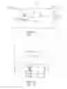
To fix the dead time inconsistency problem, the present invention proposes an amplitude normalization circuit, and the concept of which is illustrated in FIG. 3a. As illustrated in FIG. 3a, both a high amplitude full-wave rectified input voltage VFull—Wave.High and a low amplitude full-wave rectified input voltage VFull—Wave.Low are processed to generate a same normalized signal VNORM with a constant amplitude VCONST, and the same normalized signal VNORM can be used to generate a fixed dead time. Please refer to FIG. 3b, which illustrates the waveform of a normalized signal compared with a DC threshold voltage to generate a fixed dead time. As illustrated in FIG. 3b, a normalized signal VNORM is compared with a DC threshold voltage VTH to generate a normalized dead time TdN and a normalized active time TaN.
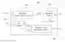
Based on the specified concept above, the present invention proposes a fixed dead time PFC controller. Please refer to FIG. 4, which illustrates the block diagram of a fixed dead time PFC controller according to a preferred embodiment of the present invention. As illustrated in FIG. 4, a fixed dead time PFC controller 400 includes an amplitude normalization circuit 401, a comparator circuit 402, a PWM/PFC circuit 403. and a driving signal selection circuit 404.
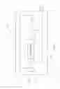
The amplitude normalization circuit 401 is used to generate a normalized signal VNORM according to a full-wave rectified input voltage VFull—Wave, wherein the amplitude of the normalized signal VNORM is constant irrespective of the amplitude of the full-wave rectified input voltage VFull—Wave. To implement the amplitude normalization circuit 401, please refer to FIG. 5. which illustrates the block diagram of the amplitude normalization circuit 401 according to a preferred embodiment of the present invention. As illustrated in FIG. 5, the amplitude normalization circuit 401, used to generate the normalized signal VNORM according to the full-wave rectified input voltage VFull—Wave, includes a variable gain amplifier 501, a peak detector 502, and an amplifier 503.
The variable gain amplifier 501 is used to amplify the full-wave rectified input voltage VFull—Wave with a gain, which is controlled by a gain control signal VGC, to generate the normalized signal VNORM.
The peak detector 502 is used to generate a peak signal VP representing the peak voltage of VNORM.
The amplifier 503 is used to generate the gain control signal VGC by amplifying the difference of VP and a DC voltage VCONST.
Due to the virtual short of the input ends of the amplifier 503 in negative feedback configuration, VP is to approach VCONST, and the amplitude of VNORM is then a constant irrespective of the amplitude of the full-wave rectified input voltage VFull—Wave.
The comparator circuit 402 is used to compare the normalized signal VNORM with a threshold voltage VTH to generate a select signal VSEL, wherein the select signal VSEL exhibits a first state (for example but not limited to a high level) when the normalized signal VNORM is higher than the threshold voltage VTH, and a second state (for example but not limited to a low level) when the normalized signal VNORM is lower than the threshold voltage VTH. The threshold voltage VTH is preferably set at a level such that the normalized dead time TdN is equal to the time the VFull—Wave of possible lowest amplitude falls below the output voltage of a power conversion application.
The PWM/PFC circuit 403 is used to generate a first driving signal VGactive. The first driving signal VGactive, when applied to a power switch, can keep the output voltage or output current of the power conversion application regulated at a DC value with the input current of the power conversion application following the hall-wave rectified input voltage VFull—Wave.
The driving signal selection circuit 404 has a first input end coupled to the first driving signal VGactive, a second input end coupled to a second driving signal VGdead, a control end coupled to the select signal VSEL, and an output end for outputting a gate driving signal VG, wherein the gate driving signal VG is provided by the first driving signal VGactive when the select signal VSEL exhibits the first state, and provided by the second driving signal VGdead when the select signal VSEL exhibits the second state. The second driving signal VGdead is preferably set at a low level.
When the fixed dead time PFC controller 400 is used in a power conversion application, a fixed dead time TdN and a fixed active time TaN (as illustrated in FIG. 3b) will be generated irrespective of the amplitude of VFull—Wave, so that the energy delivered in a period by VFull—Wave will be fixed to offer consistency in many aspects—such as power factor, average output current, etc.—of the power conversion application. For example, if the output current IO is to be regulated at a DC value ICONST, then the resulted average of the output current IO will be fixed to ICONST×TaN/(TaN+TdN) irrespective of the amplitude of VFull—Wave.
As can be seen from the specification above, by using the fixed dead time PFC controller of the present invention, a consistent performance for a power conversion application can be achieved when the power conversion application is powered by different full-wave rectified voltages of different amplitudes. Therefore, the present invention does improve the prior art controllers and is worthy of being granted a patent.
While the invention has been described by way of example and in terms of a preferred embodiment, it is to be understood that the invention is not limited thereto. To the contrary, it is intended to cover various modifications and similar arrangements and procedures, and the scope of the appended claims therefore should be accorded the broadest interpretation so as to encompass all such modifications and similar arrangements and procedures.
In summation of the above description, the present invention herein enhances the performance than the conventional structure and further complies with the patent application requirements and is submitted to the Patent and Trademark Office for review and granting of the commensurate patent rights.
Claims
What is claimed is:1. A fixed dead time PFC controller. comprising:
an amplitude normalization circuit, used to generate a normalized signal according to a full-wave rectified input voltage, wherein said normalized signal has a constant amplitude;
a comparator circuit, used to compare said normalized signal with a threshold voltage to generate a select signal, wherein said select signal exhibits a first state when said normalized signal is higher than said threshold voltage, and a second state when said normalized signal is lower than said threshold voltage; and
a driving signal selection circuit, having a first input end coupled to a first driving signal, a second input end coupled to a second driving signal, a control end coupled to said select signal, and an output end for outputting a gate driving signal, wherein said gate driving signal is provided by said first driving signal when said select signal exhibits said first state, and provided by said second driving signal when said select signal exhibits said second state.
2. The fixed dead time PFC controller as claim I, further comprising a PWM/PFC circuit to generate said first driving signal.
3. The fixed dead time PFC controller as claim 2, wherein said second driving signal is set at a low level.
4. The fixed dead time PFC controller as claim 3, wherein said amplitude normalization circuit comprises:
a variable gain amplifier, used to amplify said full-wave rectified input voltage with a gain, which is controlled by a gain control signal, to generate said normalized signal;
a peak detector, used to generate a peak signal representing the peak voltage of said normalized signal; and
an amplifier, used to generate said gain control signal by amplifying the difference of said peak signal and a DC voltage.
5. A fixed dead time PFC controller, comprising:
a variable gain amplifier, used to amplify a full-wave rectified input voltage with a gain, which is controlled by a gain control signal, to generate a normalized signal;
a peak detector, used to generate a peak signal representing the peak voltage of said normalized signal;
an amplifier, used to generate said gain control signal by amplifying the difference of said peak signal and a DC voltage;
a comparator circuit, used to compare said normalized signal with a threshold voltage to generate a select signal, wherein said select signal exhibits a first state when said normalized signal is higher than said threshold voltage, and a second state when said normalized signal is lower than said threshold voltage; and
a driving signal selection circuit, having a first input end coupled to a first driving signal, a second input end coupled to a second driving signal, a control end coupled to said select signal, and an output end for outputting a gate driving signal, wherein said gate driving signal is provided by said first driving signal when said select signal exhibits said first state, and provided by said second driving signal when said select signal exhibits said second state.
6. The fixed dead time PFC controller as claim 5, further comprising a PWM/PFC circuit to generate said first driving signal.
7. The fixed dead time PFC controller as claim 6, wherein said second driving signal is set at a low level.
8. A fixed dead time PFC controller, comprising:
a variable gain amplifier, used to amplify a full-wave rectified input voltage with a gain, which is controlled by a gain control signal, to generate a normalized signal:
a peak detector, used to generate a peak signal representing the peak voltage of said normalized signal;
an amplifier, used to generate said gain control signal by amplifying the difference of said peak signal and a DC voltage;
a comparator circuit, used to compare said normalized signal with a threshold voltage to generate a select signal, wherein said select signal exhibits a first state when said normalized signal is higher than said threshold voltage, and a second state when said normalized signal is lower than said threshold voltage;
a PWM/PFC circuit, used to generate a first driving signal; and
a driving signal selection circuit, having a first input end coupled to said first driving signal, a second input end coupled to a second driving signal, a control end coupled to said select signal, and an output end for outputting a gate driving signal, wherein said gate driving signal is provided by said first driving signal when said select signal exhibits said first state, and provided by said second driving signal when said select signal exhibits said second state.
9. The fixed dead time PFC controller as claim 8, wherein said second driving signal is set at a low level.
Images & Drawings included:

Sources:
- United States Patent and Trademark Office - verify current appl. status at the USPTO↗
Recent applications in this class:
- » 20250293593 2025-09-18
BOOST POWER SUPPLY CIRCUIT - » 20250293592 2025-09-18
BOOST POWER SUPPLY CIRCUIT - » 20250293591 2025-09-18
POWER SUPPLY CIRCUIT - » 20250293590 2025-09-18
POWER SUPPLY CIRCUIT - » 20250279718 2025-09-04
CURRENT SAMPLING METHOD AND DEVICE FOR PFC CIRCUIT, AIR CONDITIONER, AND COMPUTER-READABLE STORAGE MEDIUM - » 20250279717 2025-09-04
CONVERSION CONTROL CIRCUIT FOR ADJUSTING PFC OUTPUT VOLTAGE AND CONTROL METHOD THEREOF - » 20250253764 2025-08-07
POWER SUPPLY SYSTEM WITH POWER FACTOR CORRECTION(PFC) AND CONTROL METHOD THEREOF - » 20250202346 2025-06-19
POWER FACTOR CORRECTION CIRCUIT SWITCHING METHOD FOR REDUCING LEAKAGE CURRENT - » 20250192669 2025-06-12
POWER CONVERTER - » 20250183793 2025-06-05
METHOD FOR PWM SWITCHING OF ALTERNATING CURRENT VOLTAGE, AND HOUSEHOLD APPLIANCE IN WHICH METHOD IS EMPLOYED
Recent applications for this Assignee:
- » 20120043908 2012-02-23
LED driver controller - » 20110298390 2011-12-08
Power conversion controller having an adaptive peak current reference - » 20110285678 2011-11-24
LED driver circuit having a bias current drawn from a load current