Semiconductor module including a switching element formed of a wide bandgap semiconductor
US20130161644A1
2013-06-27
13/600,910
2012-08-31
✅ Patent granted
US 8,823,018 B2
2014-09-02
-
-
Anthony Ho
Oblon, Spivak, McClelland, Maier & Neustadt, L.L.P.
2032-08-31
Abstract:
Provided is a semiconductor module having high inrush-current tolerance. A semiconductor module includes a switching element formed of a wide bandgap semiconductor, and a free wheel diode connected in antiparallel with the switching element, wherein the free wheel diode is made of silicon and has negative temperature characteristics.
Inventors:
- Rei YONEYAMA 29 🇯🇵 Tokyo, Japan
- Hiroyuki OKABE 11 🇯🇵 Tokyo, Japan
- Takahiro INOUE 39 🇯🇵 Tokyo, Japan
- Shinji SAKAI 23 🇯🇵 Tokyo, Japan
Assignee:
- MITSUBISHI ELECTRIC CORPORATION 16,560 🇯🇵 TOKYO, Japan
Applicant:
Interested in similar patents?
Get notified when new applications in this technology area are published.
Classification:
H01L29/1608 » CPC main
Semiconductor devices adapted for rectifying, amplifying, oscillating or switching, or capacitors or resistors with at least one potential-jump barrier or surface barrier, e.g. PN junction depletion layer or carrier concentration layer; Details of semiconductor bodies or of electrodes thereof; Multistep manufacturing processes therefor; Semiconductor bodies ; Multistep manufacturing processes therefor characterised by the materials of which they are formed including, apart from doping materials or other impurities, only elements of Group IV of the Periodic System Silicon carbide
H01L25/18 » CPC further
Assemblies consisting of a plurality of individual semiconductor or other solid state devices ; Multistep manufacturing processes thereof the devices being of types provided for in two or more different subgroups of the same main group of groups -
H03K17/08142 » CPC further
Electronic switching or gating, i.e. not by contact-making and –breaking; Modifications for protecting switching circuit against overcurrent or overvoltage without feedback from the output circuit to the control circuit by measures taken in the output circuit in field-effect transistor switches
H01L2924/10254 » CPC further
Indexing scheme for arrangements or methods for connecting or disconnecting semiconductor or solid-state bodies as covered by; Details of semiconductor or other solid state devices to be connected; Material of the semiconductor or solid state bodies; Semiconducting materials; Elemental semiconductors, i.e. Group IV Diamond [C]
H01L2924/10272 » CPC further
Indexing scheme for arrangements or methods for connecting or disconnecting semiconductor or solid-state bodies as covered by; Details of semiconductor or other solid state devices to be connected; Material of the semiconductor or solid state bodies; Semiconducting materials; Compound semiconductors; IV Silicon Carbide [SiC]
H01L2924/1033 » CPC further
Indexing scheme for arrangements or methods for connecting or disconnecting semiconductor or solid-state bodies as covered by; Details of semiconductor or other solid state devices to be connected; Material of the semiconductor or solid state bodies; Semiconducting materials; Compound semiconductors; III-V Gallium nitride [GaN]
H01L2924/12031 » CPC further
Indexing scheme for arrangements or methods for connecting or disconnecting semiconductor or solid-state bodies as covered by; Details of semiconductor or other solid state devices to be connected; Device type; Passive devices, e.g. 2 terminal devices; Rectifying Diode PIN diode
H01L2924/12036 » CPC further
Indexing scheme for arrangements or methods for connecting or disconnecting semiconductor or solid-state bodies as covered by; Details of semiconductor or other solid state devices to be connected; Device type; Passive devices, e.g. 2 terminal devices; Rectifying Diode PN diode
H01L2924/13091 » CPC further
Indexing scheme for arrangements or methods for connecting or disconnecting semiconductor or solid-state bodies as covered by; Details of semiconductor or other solid state devices to be connected; Device type; Discrete devices, e.g. 3 terminal devices; Transistor; Field-effect transistor [FET] Metal-Oxide-Semiconductor Field-Effect Transistor [MOSFET]
H01L2924/0002 » CPC further
Indexing scheme for arrangements or methods for connecting or disconnecting semiconductor or solid-state bodies as covered by; Technical content checked by a classifier Not covered by any one of groups , and
H01L2924/00 » CPC further
Indexing scheme for arrangements or methods for connecting or disconnecting semiconductor or solid-state bodies as covered by
H01L29/24 IPC
Semiconductor devices adapted for rectifying, amplifying, oscillating or switching, or capacitors or resistors with at least one potential-jump barrier or surface barrier, e.g. PN junction depletion layer or carrier concentration layer; Details of semiconductor bodies or of electrodes thereof; Multistep manufacturing processes therefor; Semiconductor bodies ; Multistep manufacturing processes therefor characterised by the materials of which they are formed including, apart from doping materials or other impurities, only semiconductor materials not provided for in groups
H01L29/66068 » CPC further
Semiconductor devices adapted for rectifying, amplifying, oscillating or switching, or capacitors or resistors with at least one potential-jump barrier or surface barrier, e.g. PN junction depletion layer or carrier concentration layer; Details of semiconductor bodies or of electrodes thereof; Multistep manufacturing processes therefor; Types of semiconductor device ; Multistep manufacturing processes therefor; Multistep manufacturing processes of devices having a semiconductor body comprising crystalline silicon carbide the devices being controllable only by the electric current supplied or the electric potential applied, to an electrode which does not carry the current to be rectified, amplified or switched, e.g. three-terminal devices
H01L29/1602 » CPC further
Semiconductor devices adapted for rectifying, amplifying, oscillating or switching, or capacitors or resistors with at least one potential-jump barrier or surface barrier, e.g. PN junction depletion layer or carrier concentration layer; Details of semiconductor bodies or of electrodes thereof; Multistep manufacturing processes therefor; Semiconductor bodies ; Multistep manufacturing processes therefor characterised by the materials of which they are formed including, apart from doping materials or other impurities, only elements of Group IV of the Periodic System Diamond
H01L29/15 IPC
Semiconductor devices adapted for rectifying, amplifying, oscillating or switching, or capacitors or resistors with at least one potential-jump barrier or surface barrier, e.g. PN junction depletion layer or carrier concentration layer; Details of semiconductor bodies or of electrodes thereof; Multistep manufacturing processes therefor; Semiconductor bodies ; Multistep manufacturing processes therefor characterised by the materials of which they are formed Structures with periodic or quasi periodic potential variation, e.g. multiple quantum wells, superlattices
H01L29/6606 » CPC further
Semiconductor devices adapted for rectifying, amplifying, oscillating or switching, or capacitors or resistors with at least one potential-jump barrier or surface barrier, e.g. PN junction depletion layer or carrier concentration layer; Details of semiconductor bodies or of electrodes thereof; Multistep manufacturing processes therefor; Types of semiconductor device ; Multistep manufacturing processes therefor; Multistep manufacturing processes of devices having a semiconductor body comprising crystalline silicon carbide the devices being controllable only by variation of the electric current supplied or the electric potential applied, to one or more of the electrodes carrying the current to be rectified, amplified, oscillated or switched, e.g. two-terminal devices
H01L31/0312 IPC
Semiconductor devices sensitive to infra-red radiation, light, electromagnetic radiation of shorter wavelength or corpuscular radiation and specially adapted either for the conversion of the energy of such radiation into electrical energy or for the control of electrical energy by such radiation; Processes or apparatus specially adapted for the manufacture or treatment thereof or of parts thereof; Details thereof characterised by their semiconductor bodies characterised by the material; Inorganic materials including, apart from doping materials or other impurities, only AB compounds, e.g. SiC
H01L29/16 IPC
Semiconductor devices adapted for rectifying, amplifying, oscillating or switching, or capacitors or resistors with at least one potential-jump barrier or surface barrier, e.g. PN junction depletion layer or carrier concentration layer; Details of semiconductor bodies or of electrodes thereof; Multistep manufacturing processes therefor; Semiconductor bodies ; Multistep manufacturing processes therefor characterised by the materials of which they are formed including, apart from doping materials or other impurities, only elements of Group IV of the Periodic System
H01L29/66 IPC
Semiconductor devices adapted for rectifying, amplifying, oscillating or switching, or capacitors or resistors with at least one potential-jump barrier or surface barrier, e.g. PN junction depletion layer or carrier concentration layer; Details of semiconductor bodies or of electrodes thereof; Multistep manufacturing processes therefor Types of semiconductor device ; Multistep manufacturing processes therefor
H01L29/78 IPC
Semiconductor devices adapted for rectifying, amplifying, oscillating or switching, or capacitors or resistors with at least one potential-jump barrier or surface barrier, e.g. PN junction depletion layer or carrier concentration layer; Details of semiconductor bodies or of electrodes thereof; Multistep manufacturing processes therefor; Types of semiconductor device ; Multistep manufacturing processes therefor controllable by only the electric current supplied, or only the electric potential applied, to an electrode which does not carry the current to be rectified, amplified or switched; Unipolar devices, e.g. field effect transistors; Field effect transistors with field effect produced by an insulated gate
Description
BACKGROUND OF THE INVENTION
1. Field of the Invention
The present invention relates to a semiconductor module including a switching element formed of a wide bandgap semiconductor.
2. Description of the Background Art
As a next-generation switching element capable of realizing high withstand voltage, a low loss, and high heat resistance, a semiconductor device using silicon carbide (SiC) has been considered promising and expected to be applied to a power semiconductor module such as an inverter.
For example, Japanese Patent Application Laid-Open No. 2008-61404 proposes a current converter using a switching element formed of a wide bandgap semiconductor such as SiC.
Each switching element is connected in antiparallel with a free wheel diode in order to prevent destruction due to a surge current. In Japanese Patent Application Laid-Open No. 2010-252568, a Schottky barrier diode as a free wheel diode is formed of a wide bandgap semiconductor such as SiC, to reduce a recovery current of the free wheel diode, thus seeking reduction in switching loss.
SUMMARY OF THE INVENTION
However, when the SiC Schottky barrier diode (SiC-SBD) is used as the free wheel diode of the SiC switching element as in Japanese Patent Application Laid-Open No. 2010-252568, there has been a problem that a generated loss with respect to an inrush current is large. Since the SiC-SBD has positive temperature characteristics, when a large current flows and its temperature gets high, a forward voltage VF increases. This leads to an increase in generated loss (IF×VF) with respect to the inrush current. When the temperature of the device rises due to the increase in generated loss, the voltage VF increases, and the generated loss further increases due to the increase in VF. The device thus enters the state of such a positive feedback.
Thus, with the semiconductor module fully made of SiC which uses the free wheel diode being the SiC-SBD for the SiC switching element, there has been a problem in that the module needs to be actually used with a loss not higher than an allowable loss, and hence an operation temperature range and an inrush current value are restricted in practical use.
SUMMARY
It is an object of the present invention to provide a semiconductor module having high inrush-current tolerance.
A semiconductor module of the present invention includes a switching element and a free wheel diode. The switching element is formed of a wide bandgap semiconductor. The free wheel diode is connected in antiparallel with the switching element and made of silicon, and has negative temperature characteristics.
In the semiconductor module of the present invention, since the free wheel diode is made of silicon and has negative temperature characteristics, the diode does not enter the state of a positive feedback versus an inrush current, and thereby has high resistance.
These and other objects, features, aspects and advantages of the present invention will become more apparent from the following detailed description of the present invention when taken in conjunction with the accompanying drawings.
BRIEF DESCRIPTION OF THE DRAWINGS
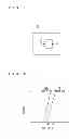
FIG. 1 is a circuit diagram of a semiconductor module according to a first preferred embodiment;
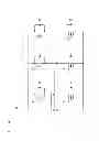
FIG. 2 is a diagram showing temperature characteristics of a free wheel diode in the semiconductor module according to the first preferred embodiment;
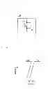
FIG. 3 is a circuit diagram of a semiconductor module according to a second preferred embodiment;
FIG. 4 is a circuit diagram of a semiconductor module according to an underlying technique;
FIG. 5 is a diagram showing temperature characteristics of a SiC Schottky barrier diode; and
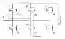
FIG. 6 is a circuit diagram of a semiconductor module according to an underlying technique.
DESCRIPTION OF THE PREFERRED EMBODIMENTS
A. Underlying Technique
FIG. 4 is a circuit diagram of a semiconductor module 100 according to an underlying technique. The semiconductor module 100 includes a SiC MOSFET 101, and a SiC Schottky barrier diode (SiC-SBD) 102 connected as a free wheel diode in antiparallel with MOSFET 101.
FIG. 5 shows a change in V-I characteristics of the SiC-SBD 102 associated with a temperature. FIG. 5 shows a V-I characteristic at the time of low temperature and a V-I characteristic at the time of high temperature. A forward voltage VF versus an inrush current IF increases to VF2 at the time of high temperature with respect to VF1 at the time of low temperature (VF1<VF2). As described above, the SiC-SBD 102 has positive temperature characteristics.
FIG. 6 shows a circuit of a converter using a plurality of semiconductor modules 100. The plurality of semiconductor modules 100 are connected in parallel with a capacitor 103. In the transient state of the capacitor 103 being charged at the time of turning on the power, an inrush current flows in a direction indicated by an arrow in FIG. 6, for example. The larger the capacity of the capacitor 103 is, the larger the value of the inrush current becomes. When a temperature of the SiC-SBD 102 rises due to the flow of the large inrush current, VF increases, and the generated loss IF×VF increases as shown in FIG. 5. When the generated loss increases, the temperature further rises, to cause an increase in VF, and when VF increases, the generated loss increases again. The diode thus enters the state of such a positive feedback.
In order to solve the above problems, a semiconductor module of the present invention has a configuration to use a device having positive temperature characteristics as a free wheel diode.
B. First Preferred Embodiment
<B-1. Configuration, Operation>
FIG. 1 is a circuit diagram of a semiconductor module 10 of a first preferred embodiment. The semiconductor module 10 includes a SiC MOSFET 11, and a Si PN diode 12 connected as a free wheel diode in antiparallel with MOSFET 11.
FIG. 2 shows a change in V-I characteristics of the PN diode 12 associated with a temperature. FIG. 2 shows a V-I characteristic at the time of low temperature and a V-I characteristic at the time of high temperature. A forward voltage VF versus a predetermined current IF decreases to VF2 at the time of high temperature with respect to VF1 at the time of low temperature (VF1>VF2). As described above, since the Si PN diode 12 has negative temperature characteristics, it has a characteristic of VF decreasing with rise in temperature. For this reason, when a large current such as an inrush current flows, a temperature of the PN diode 12 rises while its VF decreases, thereby suppressing a generated loss (IF×VF).
It is therefore possible to improve inrush-current tolerance of the semiconductor module 10 as compared with the case of using a SiC diode having positive temperature characteristics as the free wheel diode of the SiC
MOSFET 11.
<B-2. Modified Example>
It is to be noted that, although the Si PN diode 12 has been used as the free wheel diode, another diode may be used as the free wheel diode so long as it has negative temperature characteristics and, for example, a Si PiN diode may be used. In the PiN diode, providing a carrier accumulation layer in a PN junction causes occurrence of conductivity modulation, to allow a further decrease in VF than in the PN diode. It is thus possible to further improve the inrush-current tolerance of the semiconductor module than in the case of using the PN diode. Moreover, it is possible to suppress a generated loss at the time of operation, to realize a low loss.
Furthermore, a material for the MOSFET 11 as the switching element is not limited to SiC, but may be another wide bandgap semiconductor such as a gallium nitride-based material or diamond.
<B-3. Effect>
According to the semiconductor module of the present invention, the following effect is obtained. That is, the semiconductor module 10 according to the present invention includes the MOSFET 11 (switching element) formed of a wide bandgap semiconductor, and the PN diode 12 (free wheel diode) connected in antiparallel with the switching element. Since the free wheel diode is made of silicon and has negative temperature characteristics, the diode does not enter the state of the positive feedback versus the inrush current, and thereby has high resistance.
Further, since the PN diode or the PiN diode made of silicon having negative temperature characteristics is used as the free wheel diode, the diode does not enter the state of the positive feedback versus the inrush current, and thereby has high resistance.
Moreover, since the wide bandgap semiconductor constituting the MOSFET 11 contains a gallium nitride-based material or diamond other than SiC, it is possible to improve resistance to the inrush current in the semiconductor module including the switching element formed of these wide bandgap semiconductors.
C. Second Preferred Embodiment
<C-1. Configuration, Operation>
FIG. 3 is a circuit diagram of a semiconductor module 20 according to the second preferred embodiment. In the semiconductor module 20, two semiconductor modules 10 are connected in series between power connection terminals, and the two semiconductor modules 10 are further connected in three-parallel form corresponding to three-phase loads. By putting together a plurality of semiconductor modules 10 of the first preferred embodiment in one package as described above, reduction in size of the semiconductor module can be achieved.
<C-2. Effect>
The semiconductor module of the present preferred embodiment includes in one package a plurality of pairs of the switching element 11 and the free wheel diode 12 of the first preferred embodiment, whereby reduction in size of the semiconductor module can be achieved.
While the invention has been shown and described in detail, the foregoing description is in all aspects illustrative and not restrictive. It is therefore understood that numerous modifications and variations can be devised without departing from the scope of the invention.
Claims
What is claimed is:1. A semiconductor module comprising:
a switching element formed of a wide bandgap semiconductor; and
a free wheel diode connected in antiparallel with said switching element, wherein
said free wheel diode is made of silicon and has negative temperature characteristics.
2. The semiconductor module according to claim 1, wherein said free wheel diode is a PN diode or a PiN diode.
3. The semiconductor module according to claim 1, wherein said wide bandgap semiconductor contains silicon carbide, a gallium nitride-based material, or diamond.
4. The semiconductor module according to claim 1, comprising a plurality of pairs of said switching element and said free wheel diode in one package.
Images & Drawings included:

Sources:
- United States Patent and Trademark Office - verify current appl. status at the USPTO↗
Recent applications in this class:
- » 20130171403 2013-07-04
Production method for an SiC volume monocrystal with a non-homogeneous lattice plane course and a monocrystalline SiC substrate with a non-homogeneous lattice plane course - » 20130056752 2013-03-07
SILICON CARBIDE SUBSTRATE, SILICON CARBIDE SUBSTRATE MANUFACTURING METHOD, AND SEMICONDUCTOR DEVICE MANUFACTURING METHOD - » 20130049013 2013-02-28
Semiconductor device, electro-optic device, power conversion device, and electronic apparatus - » 20130032809 2013-02-07
Semiconductor devices with non-implanted barrier regions and methods of fabricating same - » 20130020611 2013-01-24
Bipolar junction transistor with stair profile - » 20130020586 2013-01-24
Semiconductor device
Recent applications for this Assignee:
- » 20250294680 2025-09-18
POWER MODULE - » 20250293740 2025-09-18
WIRELESS COMMUNICATION SYSTEM - » 20250293196 2025-09-18
SEMICONDUCTOR DEVICE AND MANUFACTURING METHOD THEREOF - » 20250291113 2025-09-18
OPTICAL TERMINATOR, OPTICAL WAVELENGTH FILTER, AND EXTERNAL CAVITY LASER LIGHT SOURCE - » 20250290867 2025-09-18
SEMICONDUCTOR INSPECTION APPARATUS AND METHOD OF MANUFACTURING SEMICONDUCTOR DEVICE - » 20250290765 2025-09-18
INFORMATION PROCESSING DEVICE, INFORMATION PROCESSING METHOD, AND IMAGE PROJECTING SYSTEM - » 20250289592 2025-09-18
SPACE SITUATIONAL AWARENESS BUSINESS DEVICE AND SPACE TRAFFIC BUSINESS DEVICE - » 20250287683 2025-09-11
SEMICONDUCTOR DEVICE - » 20250287624 2025-09-11
POWER SEMICONDUCTOR DEVICE - » 20250287098 2025-09-11
DETECTION DEVICE, CAMERA SYSTEM, DETECTION METHOD, AND STORAGE MEDIUM STORING DETECTION PROGRAM