Circuit for filtering narrow pulse and compensating wide pulse, and motor controller comprising the circuit
US20130214715A1
2013-08-22
13/845,058
2013-03-17
✅ Patent granted
US 9,018,874 B2
2015-04-28
-
-
Paul Ip
Matthias Scholl P.C. | Matthias Scholl
2033-08-15
Abstract:
A circuit for filtering narrow pulse and compensating wide pulse, including a signal shaping circuit, a filter circuit, and a pulse width compensating circuit. The signal shaping circuit processes an input signal and transmits the input signal to the filter circuit. The filter circuit filters off narrow pulses of the input signal. The pulse width compensating circuit compensates the wide pulses of the input signal and outputs an output signal.
Inventors:
- Yuefei GUO 1 🇨🇳 Beijing, China
- Zhouping LIN 1 🇨🇳 Beijing, China
- Chong YU 1 🇨🇳 Beijing, China
- Jun KANG 1 🇨🇳 Beijing, China
- Kun CHENG 4 🇨🇳 Beijing, China
- BROAD-OCEAN MOTOR EV CO., LTD. 1 🇺🇸 , United States
Assignee:
- BROAD-OCEAN MOTOR EV CO., LTD. 4 🇨🇳 Beijing, China
Applicant:
Interested in similar patents?
Get notified when new applications in this technology area are published.
Classification:
H02P27/08 » CPC further
Arrangements or methods for the control of AC motors characterised by the kind of supply voltage using variable-frequency supply voltage, e.g. inverter or converter supply voltage using dc to ac converters or inverters with pulse width modulation
H03K3/017 » CPC main
Circuits for generating electric pulses; Monostable, bistable or multistable circuits; Details Adjustment of width or dutycycle of pulses
H02P6/14 IPC
Arrangements for controlling synchronous motors or other dynamo-electric motors using electronic commutation dependent on the rotor position; Electronic commutators therefor Electronic commutators
H02M1/32 » CPC further
Details of apparatus for conversion Means for protecting converters other than automatic disconnection
H02M7/5387 IPC
Conversion of ac power input into dc power output; Conversion of dc power input into ac power output; Conversion of dc power input into ac power output without possibility of reversal by static converters using discharge tubes with control electrode or semiconductor devices with control electrode using devices of a triode or transistor type requiring continuous application of a control signal using semiconductor devices only, e.g. single switched pulse inverters in a bridge configuration
H02M7/5395 » CPC further
Conversion of ac power input into dc power output; Conversion of dc power input into ac power output; Conversion of dc power input into ac power output without possibility of reversal by static converters using discharge tubes with control electrode or semiconductor devices with control electrode using devices of a triode or transistor type requiring continuous application of a control signal using semiconductor devices only, e.g. single switched pulse inverters with automatic control of output wave form or frequency by pulse-width modulation
Description
CROSS-REFERENCE TO RELATED APPLICATIONS
This application is a continuation-in-part of International Patent Application No. PCT/CN2011/085119 with an international filing date of Dec. 31, 2011, designating the United States, now pending, the contents of which are incorporated herein by reference. Inquiries from the public to applicants or assignees concerning this document or the related applications should be directed to: Matthias Scholl P.C., Attn.: Dr. Matthias Scholl Esq., 14781 Memorial Drive, Suite 1319, Houston, Tex. 77079.
BACKGROUND OF THE INVENTION
1. Field of the Invention
The invention relates to a circuit for filtering narrow pulse and compensating wide pulse.
2. Description of the Related Art
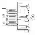
As shown in FIG. 1, a typical permanent magnet synchronous motor controller includes a PWM signal generator, an inverter unit, and a motor body (M). The motor body (M) includes a permanent magnet rotor, a stator, and windings (U, V, and W). The PWM signal generator can adopt a micro controller unit (MCU) or a special integrated circuit chip IC, and generate pulse signals of a certain width, so that the insulated gate bipolar transistors IGBT (Q1, Q2, Q3, Q4, Q5, and Q6) of the inverter unit are conducted by turns, and the windings (U, V, and W) are powered on by turns.
During the treatment process of the conventional motor controller, driving signals used for controlling the IGBT and calculated through the PWM signal generator (i.e., micro controller unit (MCU)) under the action of modulation and demodulation from software include narrow pulses. The narrow pulses have negative effects on the IGBT (Insulated Gate Bipolar Transistor). As shown in FIG. 2, before the PWM signal generator generates normal drive pulses B, a plurality of narrow pulses will be generated. These narrow pulses A will be closed immediately before the complete opening of the IGBT, the IGBT will be overheated, thus the service life will be affected, the IGBT will be destroyed after a long time of use, even the IGBT will be burned out, and the negative impact to motor control will be caused. Therefore, the modulated pulses are required to be treated.
SUMMARY OF THE INVENTION
In view of the above-described problems, it is one objective of the invention to provide a circuit for filtering narrow pulse and compensating wide pulse. The circuit can filter off narrow pulses of an input signal and allow normal pulses to pass completely.
To achieve the above objective, in accordance with one embodiment of the invention, there is provided a circuit for filtering narrow pulse and compensating wide pulse, comprising a signal shaping circuit, a filter circuit, and a pulse width compensating circuit. The signal shaping circuit processes an input signal and transmits the input signal to the filter circuit. The filter circuit filters off narrow pulses of the input signal, and wide pulses of the input signal are compensated from the pulse width compensating circuit and output.
In a class of this embodiment, the filter circuit is an RC filter circuit.
In a class of this embodiment, the signal shaping circuit comprises a first Schmitt trigger.
In a class of this embodiment, the pulse width compensating circuit comprises a second Schmitt trigger, a triode, a first resistor, a second resistor, and a capacitor. The input signal processed through the filter circuit is connected with the second Schmitt trigger. The signal is output from an output end of the second Schmitt trigger. The capacitor and the second resistor are connected in series and connected to the output end and a grounded end of the second Schmitt trigger respectively. A node between the capacitor and the second resistor is connected with a base electrode of the triode after being connected with the first resistor. An emitting electrode of the triode is grounded, and a collecting electrode of the triode is connected with an input end of the Second Schmitt trigger.
Advantages of the circuit for filtering narrow pulse and compensating wide pulse are summarized as follows:
-
- (1) the narrow pulses of the input signal can be filtered off, the normal pulses can completely pass, the control is more accurate, and the electronic components for a downstream circuit are protected effectively;
- (2) the filter circuit is an RC filter circuit, the signal shaping circuit is a Schmitt trigger, and the two circuits are matched with each other, thus the circuit structure is simple and reasonable, and the narrow pulses can be filtered off effectively; and
- (3) the pulse width compensating circuit comprises a Schmitt trigger, a triode, a resistor and a capacitor; the circuit structure is simple and reliable, and the manufacturing cost is low.
Another objective of the invention is to provide a motor controller. A circuit for filtering narrow pulse and compensating wide pulse is accessed between the PWM (Pulse-Width Modulation) signal generator and the inverter unit, and can filter off the narrow pulses in a signal input from the PWM signal generator and allow the normal pulses to completely pass. The pulses input into the inverter unit all become normal pulses. Thus, the power element IGBT is protected effectively, and the control is more accurate.
In accordance with another embodiment of the invention, there provided is a motor controller, comprising a PWM signal generator and an inverter unit. The PWM signal generator comprises a plurality of signal output ends, each of the signal output ends being provided with a circuit for filtering narrow pulse and compensating wide pulse, an output end of the circuit for filtering narrow pulse and compensating wide pulse being connected with an input end of the inverter unit. The circuit for filtering narrow pulse and compensating wide pulse comprises a signal shaping circuit, a filter circuit, and a pulse width compensating circuit. The signal shaping circuit processes an input signal and transmits the input signal to the filter circuit. The filter circuit filters off narrow pulses of the input signal, and wide pulses of the input signal are compensated from the pulse width compensating circuit and output.
In a class of this embodiment, the filter circuit is an RC filter circuit.
In a class of this embodiment, the signal shaping circuit comprises a first Schmitt trigger.
In a class of this embodiment, the pulse width compensating circuit comprises a second Schmitt trigger, a triode, a first resistor, a second resistor, and a capacitor. The input signal processed through the filter circuit is connected with the second Schmitt trigger. The signal is output from an output end of the second Schmitt trigger. The capacitor and the second resistor are connected in series and connected to the output end and a grounded end of the second Schmitt trigger respectively. A node between the capacitor and the second resistor is connected with a base electrode of the triode after being connected with the first resistor. An emitting electrode of the triode is grounded, and a collecting electrode of the triode is connected with an input end of the Second Schmitt trigger.
Advantages of the motor controller are summarized as follows:
-
- (1) the circuit for filtering narrow pulse and compensating wide pulse is accessed between the PWM signal generator and the inverter unit, and can filter off the narrow pulses in a signal input from the PWM signal generator and allow the normal pulses to completely pass, and the pulses input into the inverter unit all become normal pulses, thus the power element IGBT is protected effectively, and the control is more accurate;
- (2) the filter circuit is an RC filter circuit, the signal shaping circuit is a Schmitt trigger, and the two circuits are matched with each other, thus the circuit structure is simple and reasonable, and the narrow pulses can be filtered off effectively; and
- (3) the pulse width compensating circuit comprises a Schmitt trigger, a triode, a resistor and a capacitor, the circuit structure is simple and reliable, and the manufacturing cost is low.
BRIEF DESCRIPTION OF THE DRAWINGS
FIG. 1 is a partial functional block diagram of a traditional motor controller;
FIG. 2 is a diagram for signals generated from a traditional PWM signal generator;
FIG. 3 is a functional block diagram of a circuit for filtering narrow pulse and compensating wide pulse of the invention;
FIG. 4 is a corresponding circuit diagram of FIG. 3; and
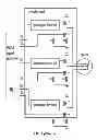
FIG. 5 is a principle diagram of a motor controller of the invention.
DETAILED DESCRIPTION OF THE EMBODIMENTS
The following specific embodiments and drawings aim to serve as the further description for the invention.
As shown in FIG. 3 and FIG. 4, a circuit for filtering narrow pulse and compensating wide pulse comprises a signal shaping circuit 1, a filter circuit 2, and a pulse width compensating circuit 3. An input signal processed through the signal shaping circuit 1 is transmitted to the filter circuit 2. The filter circuit 2 filters off the narrow pulses of the input signal, and the wide pulses of the input signal are output after compensation from the pulse width compensating circuit 3. The signal shaping circuit 1 comprises a first Schmitt trigger IC1A and a resistor R1. The resistor R1 is connected between the input end of the first Schmitt trigger IC1A and the ground respectively, and the input signal is connected at the input end of the first Schmitt trigger IC1A. The filter circuit 2 is an RC filter circuit and comprises a resistor R2 and a capacitor C1. The pulse width compensating circuit 3 comprises a second Schmitt trigger IC1B, a triode Q1, a first resistor R3, a second resistor R4 and a capacitor C2. The input signal processed through the filter circuit 2 is connected with the second Schmitt trigger IC1B. The signal is output from the output end of the second Schmitt trigger IC1B, after the capacitor C2 is connected with the second resistor R4 in series, two ends of the capacitor C2 are connected at the output end and the grounded end of the second Schmitt trigger IC1B respectively. A node between the capacitor C2 and the second resistor R4 is connected with a base electrode of the triode Q1 after being connected with the first resistor R3. An emitting electrode of the triode Q1 is grounded, and a collecting electrode of the triode Q1 is connected with the input end of the second Schmitt trigger IC1B. The resistor R2 is connected between the output end of the first Schmitt trigger IC1A and the input end of the second Schmitt trigger IC1B, one end of the capacitor C1 is connected between the resistor R2 and the input end of the second Schmitt trigger IC1B, and the other end of the capacitor C1 is grounded.
The principle of the invention is as follows: as shown in FIG. 3 and FIG. 4, the input signal is driven to enter into the signal shaping circuit 1 from an IN end, and then reaches the filter circuit 2 after shaping and anti jamming processing from the resistor R1 and the first Schmitt trigger IC1A, and it is assumed that the pulse width of the driven input signal at the moment is Ti. The resistor R2 and the capacitor C1 constitute a narrow pulse filter circuit, and the width of pulses filtered through the filter circuit is T1, thus the pulse width of the driven input signal to reach the pulse width compensating circuit 3 is Ti−T1. When Ti−T1≦0, narrow pulses are totally absorbed, and the second Schmitt trigger IC1B outputs low level, that is, the position 4 is in low level. When Ti−T1>0, pulses are not totally absorbed, and the second Schmitt trigger IC1B outputs high level, that is, the position 4 is in high level. A triode Q1 in an inverter is conducted. A compensating circuit comprising a triode Q1, a capacitor C2, a first resistor R3 and a second resistor R4 is used for compensating pulses. The width of pulses compensated through the compensating circuit is set as T2. The overall width of the compensated pulses is Ti−T1+T2. When the relationship that the pulse width of the signal at the output end OUT is T0=Ti is met, T1=T2, and it's realized through setting the values of the resistor R2, the capacitor C1, the capacitor C2, the first resistor R3 and the second resistor R4, thus T0=Ti under the application of the compensating circuit, that is, after the pulse width exceeds the minimum pulse width, the pulses are output in an intact state; the harmless pulses with driving capability are reserved but not the harmful pulses with narrower width, thus the purposes of preventing the IGBT from being overheated and protecting the IGBT are achieved ultimately. For example, when the width of the narrow pulses is smaller than the minimum pulse width T1, it's assumed as 3 microseconds, the assumed width of the narrow pulses of the input signal is only 2 microseconds, then the narrow pulses will be filtered off; if the pulses with width of 3.5 microseconds are contained in the input signal, they will be reversed and output.
As shown in FIG. 3, FIG. 4, and FIG. 5, a motor controller comprises a PWM signal generator and an inverter unit. A circuit for filtering narrow pulse and compensating wide pulse is installed at a plurality of signal output ends of the PWM signal generator, and the output end of the circuit for filtering narrow pulse and compensating wide pulse is connected with the input end of the inverter unit. The circuit for filtering narrow pulse and compensating wide pulse comprises a signal shaping circuit 1, a filter circuit 2 and a pulse width compensating circuit 3. The input signal processed through the signal shaping circuit 1 is transmitted to the filter circuit 2. The filter circuit 2 filters off the narrow pulses of the input signal, and the wide pulses of the input signal are output after compensation from the pulse width compensating circuit 3. The signal shaping circuit 1 comprises a first Schmitt trigger IC1A and a resistor R1. The resistor R1 is connected between the input end of the first Schmitt trigger IC1A and the ground respectively, and the input signal is connected at the input end of the first Schmitt trigger IC1A. The filter circuit 2 is an RC filter circuit and comprises a resistor R2 and a capacitor C1. The pulse width compensating circuit 3 comprises a second Schmitt trigger IC1B, a triode Q1, a first resistor R3, a second resistor R4 and a capacitor C2. The input signal processed through the filter circuit 2 is connected with the second Schmitt trigger IC1B, the signal is output from the output end of the second Schmitt trigger IC1B, after the capacitor C2 is connected with the second resistor R4 in series, two ends of the capacitor C2 are connected at the output end and the grounded end of the second Schmitt trigger IC1B respectively. A node between the capacitor C2 and the second resistor R4 is connected with a base electrode of a triode Q1 after being connected with the first resistor R3. An emitting electrode of the triode Q1 is grounded. A collecting electrode of the triode Q1 is connected with the input end of the second Schmitt trigger IC1B. The resistor R2 is connected between the output end of the first Schmitt trigger IC1A and the input end of the second Schmitt trigger IC1B. One end of the capacitor C1 is connected between the resistor R2 and the input end of the second Schmitt trigger IC1B, and the other end of the capacitor C1 is grounded.
The a circuit for filtering narrow pulse and compensating wide pulse is accessed between the PWM signal generator and the inverter unit, and can filter off the narrow pulses in the signal output from the PWM signal generator and allow the normal pulses to pass completely, and the pulses input to the inverter unit all become normal pulses. Thus, the power element IGBT is protected effectively, and the control is more accurate.
Claims
The invention claimed is:1. A circuit for filtering narrow-pulse and compensating wide pulse, the circuit comprising:
a) a signal shaping circuit (1);
b) a filter circuit (2); and
c) a pulse width compensating circuit (3);
wherein
the signal shaping circuit (1) processes an input signal and transmits the input signal to the filter circuit (2);
the filter circuit (2) filters off narrow pulses of the input signal; and
the pulse width compensating circuit (3) compensates wide pulses of the input signal and outputs an output signal.
2. The circuit of claim 1, wherein the filter circuit (2) is an RC filter circuit.
3. The circuit of claim 1, wherein the signal shaping circuit (1) comprises a first Schmitt trigger (IC1A).
4. The circuit of claim 2, wherein the signal shaping circuit (1) comprises a first Schmitt trigger (IC1A).
5. The circuit of claim 3, wherein
the pulse width compensating circuit (3) comprises a second Schmitt trigger (IC1B), a triode (Q1), a first resistor (R3), a second resistor (R4), and a capacitor (C2);
the input signal processed through the filter circuit (2) is connected with the second Schmitt trigger (IC1B);
the signal is output from an output end of the second Schmitt trigger (IC1B);
the capacitor (C2) and the second resistor (R4) are connected in series and connected to the output end and a grounded end of the Second Schmitt trigger (IC1B), respectively;
a node between the capacitor (C2) and the second resistor R4 is connected with a base electrode of the triode (Q1) after being connected with the first resistor (R3);
an emitting electrode of the triode (Q1) is grounded; and
a collecting electrode of the triode (Q1) is connected with an input end of the Second Schmitt trigger (IC1B).
6. The circuit of claim 4, wherein
the pulse width compensating circuit (3) comprises a second Schmitt trigger (IC1B), a triode (Q1), a first resistor (R3), a second resistor (R4), and a capacitor (C2);
the input signal processed through the filter circuit (2) is connected with the second Schmitt trigger (IC1B);
the signal is output from an output end of the second Schmitt trigger (IC1B);
the capacitor (C2) and the second resistor (R4) are connected in series and connected to the output end and a grounded end of the Second Schmitt trigger (IC1B), respectively;
a node between the capacitor (C2) and the second resistor R4 is connected with a base electrode of the triode (Q1) after being connected with the first resistor (R3);
an emitting electrode of the triode (Q1) is grounded; and
a collecting electrode of the triode (Q1) is connected with an input end of the Second Schmitt trigger (IC1B).
7. A motor controller, comprising a PWM signal generator and an inverter unit, the PWM signal generator comprising a plurality of signal output ends, each of the signal output ends being provided with a circuit for filtering narrow-pulse and compensating wide pulse, an output end of the circuit for filtering narrow-pulse and compensating wide pulse being connected with an input end of the inverter unit, wherein
the circuit for filtering narrow-pulse and compensating wide pulse comprises a signal shaping circuit (1), a filter circuit (2), and a pulse width compensating circuit (3);
the signal shaping circuit (1) processes an input signal and transmits the input signal to the filter circuit (2);
the filter circuit (2) filters off narrow pulses of the input signal; and
the pulse width compensating circuit (3) compensates the wide pulses of the input signal and outputs an output signal.
8. The motor controller of claim 7, wherein the filter circuit (2) is an RC filter circuit.
9. The motor controller of claim 7, wherein the signal shaping circuit (1) comprises a first Schmitt trigger (IC1A).
10. The motor controller of claim 8, wherein the signal shaping circuit (1) comprises a first Schmitt trigger (IC1A).
11. The motor controller of claim 9, wherein
the pulse width compensating circuit (3) comprises a second Schmitt trigger (IC1B), a triode (Q1), a first resistor (R3), a second resistor (R4), and a capacitor (C2);
the input signal processed through the filter circuit (2) is connected with the second Schmitt trigger (IC1B);
the signal is output from an output end of the second Schmitt trigger (IC1B);
the capacitor (C2) and the second resistor (R4) are connected in series and connected to the output end and a grounded end of the Second Schmitt trigger (IC1B), respectively;
a node between the capacitor (C2) and the second resistor R4 is connected with a base electrode of the triode (Q1) after being connected with the first resistor (R3);
an emitting electrode of the triode (Q1) is grounded; and
a collecting electrode of the triode (Q1) is connected with an input end of the Second Schmitt trigger (IC1B).
12. The motor controller of claim 10, wherein
the pulse width compensating circuit (3) comprises a second Schmitt trigger (IC1B), a triode (Q1), a first resistor (R3), a second resistor (R4), and a capacitor (C2);
the input signal processed through the filter circuit (2) is connected with the second Schmitt trigger (IC1B);
the signal is output from an output end of the second Schmitt trigger (IC1B);
the capacitor (C2) and the second resistor (R4) are connected in series and connected to the output end and a grounded end of the Second Schmitt trigger (IC1B), respectively;
a node between the capacitor (C2) and the second resistor R4 is connected with a base electrode of the triode (Q1) after being connected with the first resistor (R3);
an emitting electrode of the triode (Q1) is grounded; and
a collecting electrode of the triode (Q1) is connected with an input end of the Second Schmitt trigger (IC1B).
Images & Drawings included:


Sources:
- United States Patent and Trademark Office - verify current appl. status at the USPTO↗
Recent applications in this class:
- » 20250293671 2025-09-18
ELECTRONIC CIRCUITRY, DRIVE CIRCUIT, AND CONTROL SYSTEM - » 20250286539 2025-09-11
Pulse Width Control Apparatus and Method - » 20250286538 2025-09-11
CONTROL DEVICE, ELECTRONIC DEVICE, AND CONTROL METHOD CAPABLE OF REDUCING NUMBER OF OUTPUT TERMINALS OF PROCESSOR EXECUTING DATA COMMUNICATION WITH INTEGRATED CIRCUIT - » 20250274107 2025-08-28
ADAPTIVE VARIABLE CYCLE ELECTROLYSIS CONTROL DEVICE - » 20250226816 2025-07-10
Multi-Axis Drive Control Circuit - » 20250211209 2025-06-26
DUTY CYCLE CALIBRATION CIRCUIT AND METHOD, CHIP, AND ELECTRONIC DEVICE - » 20250167771 2025-05-22
DUTY CYCLE SIGNAL PROCESSING CIRCUIT AND METHOD, AND AUDIO SIGNAL PROCESSING DEVICE - » 20250167770 2025-05-22
CIRCUIT AND METHOD FOR DUTY CYCLE ADJUSTMENT - » 20250132754 2025-04-24
SEMICONDUCTOR BURN-IN MACHINE POWER REGULATOR HAVING MULTIPLE POWER MODES - » 20250088178 2025-03-13
VOLTAGE REGULATOR
Recent applications for this Assignee:
- » 20230043468 2023-02-09
Method for controlling fuel cell - » 20210013528 2021-01-14
Fuel cell - » 20170033622 2017-02-02
Punching sheet used for manufacturing rotor and permanent magnet motor comprising rotor