METHOD FOR MANUFACTURING LIGHT EMITTING DIODE
US20130288409A1
2013-10-31
13/726,193
2012-12-23
Abstract:
An exemplary method for manufacturing an LED includes steps: providing a substrate with a first electrode and a second electrode; providing an isosceles trapezoidal LED chip and making the LED chip electrically connecting the first electrode and the second electrode; providing a mold with a cavity and setting the mold on the substrate to make the LED chip received in the cavity, an outer periphery of the LED chip spaced from confronting edges of the mold defining the cavity to define a channel therebetween, and a width of the channel being uniform; providing phosphor glue and filling the phosphor glue in the channel to make the phosphor glue enclose the LED chip therein; solidifying the phosphor glue to form a phosphor layer covering the LED chip and removing the mold.
Inventors:
- PIN-CHUAN CHEN 62 🇹🇼 Hsinchu, Taiwan
- HSIN-CHIANG LIN 29 🇹🇼 Hsinchu, Taiwan
- Advanced Optoelectronic Technology, Inc. 16 🇺🇸 , United States
Assignee:
- ADVANCED OPTOELECTRONIC TECHNOLOGY, INC. 420 🇹🇼 Hsinchu Hsien, Taiwan
Interested in similar patents?
Get notified when new applications in this technology area are published.
Classification:
H01L33/44 » CPC main
Semiconductor devices with at least one potential-jump barrier or surface barrier specially adapted for light emission; Processes or apparatus specially adapted for the manufacture or treatment thereof or of parts thereof; Details thereof characterised by the coatings, e.g. passivation layer or anti-reflective coating
Description
BACKGROUND
1. Technical Field
The present disclosure relates to semiconductor devices and, more particularly, to a method for manufacturing a light emitting diode (LED).
2. Description of Related Art
LEDs have many beneficial characteristics, including low electrical power consumption, low heat generation, long lifetime, small volume, good impact resistance, fast response and excellent stability. These characteristics have enabled the LEDs to be widely used as a light source in electrical appliances and electronic devices.
A conventional method for manufacturing an LED includes following steps: providing a substrate with an LED chip mounted thereon, and dispensing phosphor glue mixed by glue and phosphor on the substrate and enclosing the LED chip therein. Light emitted from the LED chip excites the phosphor in the phosphor glue to emit a light of a different wavelength, which mixes the light from the LED chip obtain a light having a desired color. The phosphor glue is prone to be accumulated on a bottom end at lateral sides of the LED chip due to gravity before solidified. Therefore, a thickness of the phosphor glue at a top end of LED chip is less than that at the lateral sides of the LED chip, which results in an unevenly light output at the top end and the lateral sides of the LED chip during operation of the LED.
What is needed is a method for manufacturing an LED which can overcome the problem of the prior art.
BRIEF DESCRIPTION OF THE DRAWINGS
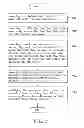
FIG. 1 is a flowchart of a method for manufacturing an LED in accordance with an exemplary embodiment of the present disclosure.
FIGS. 2-7 are schematic views showing steps of the method for manufacturing the LED of FIG. 1.
FIG. 8 is an enlarged view of a circled portion VIII of FIG. 7.
DETAILED DESCRIPTION
Referring to FIG. 1, a method for manufacturing an LED (shown in FIGS. 7 & 8) in accordance with an exemplary embodiment of the present disclosure includes the following steps.
Referring also to FIG. 2, a step S11 is providing a substrate 10 and forming a first electrode 11 and a second electrode 13 on the substrate 10. The substrate 10 includes a top surface 101a and a bottom surface 101b opposite to the top surface 101a. The first electrode 11 is formed on a left side of the top surface 101a and extends to a left side of the bottom surface 101b from a left end of the substrate 10. The second electrode 13 is formed on a right side of the top surface 101a and extends to a right side of the bottom surface 101b from a right end of the substrate 10. The first electrode 11 and the second electrode 13 are spaced from each other. A receiving hole 20 is defined by inner ends of the first electrode 11, the second electrode 13 and the top surface 101a of the substrate 10. The substrate 10 is electrically insulating and made of ceramic or silicon.
Referring to FIG. 3, a step S12 is providing an LED chip 30 and mounting the LED chip 30 on the substrate 10 to make the LED chip 30 electrically connect the first electrode 11 and the second electrode 13. The LED chip 30 includes a top surface 301, a bottom surface 303 and a side wall 302 connecting the top surface 301 and the bottom surface 303. The top surface 301 is parallel to the bottom surface 303. The LED chip 30 has an isosceles trapezoidal cross section along a height direction thereof. A transverse width of the LED chip 30 increases from the top surface 301 to the bottom surface 303 along the height direction of the LED chip 30. A first electrical connecter 305 and a second electrical connecter 307 are protruded from the bottom surface 303 of the LED chip 30. The first electrical connecter 305 and the second electrical connecter 307 are spaced from each other and respectively electrically contact the first electrode 11 and the second electrode 13. The first and second electrical connectors 305, 307 are solder balls. The LED chip 30 is located at a top side of the receiving hole 20. The bottom surface 303 is spaced from the first electrode 11 and the second electrode 13.
Referring to FIG. 4, a step S13 is providing a mold 40 with a cavity 41 therein, and setting the mold 40 on top surfaces of the first electrode 11 and the second electrode 13 to make the LED chip 30 received in a center of a bottom of the cavity 41. The cavity 41 has an isosceles trapezoidal cross section along a height direction thereof. A transverse width of the cavity 41 of the mold 40 increases from top to bottom. When the LED chip 30 is received in the center of the bottom of the cavity 41, a channel 43 is defined between an outer periphery of the LED chip 30 and confronting edges of the mold 40 defining the cavity 41. A distance between a top of the mold 40 and the top surface 301 (i.e., a depth of the channel 43 above the top surface 301) is equal to a distance between each of the confronting edges of the mold defining the cavity 41 to the correspondingly adjacent side wall 303.
Referring to FIGS. 5-6, a step S14 is providing phosphor glue 60 and filling the phosphor glue 60 in the channel 43. The phosphor glue 60 is formed by transparent glue and phosphor. The phosphor and the transparent glue are evenly mixed. A scraper 70 is provided to slide along a top surface of the mold 40 to scrape a part of the phosphor glue 60 which is higher beyond the top surface of the mold 40. The phosphor glue 60 also fills in the receiving hole 20 to increase a contact area between the phosphor glue 60 LED chip 30 and to increase the binding force between the LED chip 30 and the substrate 10.
Referring to FIGS. 7-8, a step S15 is solidifying the phosphor glue 60 rapidly to form a phosphor layer 61 covering the LED chip 30 and removing the mold 40 from the phosphor glue 60 and the substrate 10. Thus, the LED is manufactured completely. Because the distance between the top of the mold 40 and the top surface 301 of the LED chip 30 is equal to the distance between the confronting edges of the mold 40 defining the cavity 41 and the side walls 303 of the LED chip 30, a thickness of the phosphor layer 61 on the top surface 301 and the side walls 303 of the LED chip 30 is uniform.
It is understood that, in this embodiment, the thickness of the phosphor layer 61 is uniform, so a light intensity of light from a top side and lateral sides f the LED is uniform.
It is to be further understood that even though numerous characteristics and advantages of the present embodiments have been set forth in the foregoing description, together with details of the structures and functions of the embodiments, the disclosure is illustrative only, and changes may be made in detail, especially in matters of shape, size, and arrangement of parts within the principles of the disclosure to the full extent indicated by the broad general meaning of the terms in which the appended claims are expressed.
Claims
What is claimed is:1. A method for manufacturing an LED (light emitting diodes) comprising following steps:
providing a substrate with a first electrode and a second electrode thereon;
providing an isosceles trapezoidal LED chip on the substrate and electrically connecting the LED chip to the first electrode and the second electrode;
providing a mold with a cavity and setting the mold on the substrate to make the LED chip received in a center of a bottom of the cavity, a channel being defined between confronting edges of the mold defining the cavity and a side wall and a top surface of the LED chip;
providing phosphor glue and filling the phosphor glue in the cavity to make the phosphor glue fill in the channel and enclose the LED chip therein;
solidifying the phosphor glue to form a phosphor layer covering the LED chip; and
removing the mold, a thickness of the phosphor layer on the top surface of the LED chip and on the side wall of the LED chip being uniform.
2. The method as claimed in claim 1, wherein a scraper is provided before the phosphor glue is solidified to scrape a part of the phosphor glue higher beyond a top surface of the mold.
3. The method as claimed in claim 1, wherein the phosphor glue is mixed by transparent glue and phosphor.
4. The method as claimed in claim 3, wherein the phosphor powder and the transparent glue are evenly mixed.
5. The method as claimed in claim 1, wherein a first electrical connecter and a second electrical connecter are protruded from a bottom surface of the LED chip and respectively electrically connect the first electrode and the second electrode.
6. The method as claimed in claim 5, wherein the first electrode is formed on a left side of the top surface and extends to a left side of the bottom surface from a left end of the substrate, the second electrode is formed on a right side of the top surface and extends to a right side of the bottom surface from a right end of the substrate.
7. The method as claimed in claim 6, wherein the bottom surface of the LED chip is located at a top of the first and second electrodes, a receiving hole is defined between the first and second electrodes and the bottom surface of the LED chip, and when the phosphor glue is filled in the cavity, the phosphor glue also fills in the receiving hole.
8. A method for manufacturing an LED (light emitting diode) comprising following steps:
providing a first electrode and a second electrode electrically insulating from the first electrode;
providing an isosceles trapezoidal LED chip and electrically connecting the LED chip with the first electrode and the second electrode;
providing a mold with a cavity and setting the mold on the first and second electrodes to make the LED chip received in the cavity, an outer periphery of the LED chip being spaced from confronting edges of the mold defining the cavity to define a channel therebetween, and a width of the channel being uniform;
providing phosphor glue and filling the phosphor glue in the channel to make the phosphor glue enclose the LED chip therein; and
solidifying the phosphor glue to form a phosphor layer covering the LED chip and removing the mold.
9. The method as claimed in claim 8, wherein a scraper is provided before the phosphor glue is solidified to scrape a part of the phosphor glue overflowed from the cavity of the mold.
10. The method as claimed in claim 8, wherein the phosphor glue is mixed by transparent glue and phosphor.
12. The method as claimed in claim 8, wherein a first electrical connecter and a second electrical connecter are protruded from the LED chip and respectively electrically connect the first electrode and the second electrode.
Images & Drawings included:


Sources:
- United States Patent and Trademark Office - verify current appl. status at the USPTO↗
Similar patent applications:
- » 20080210957
Light emitting diode, method for manufacturing light emitting diode, integrated light emitting diode, method for manufacturing integrated light emitting diode, light emitting diode backlight, light emitting diode illumination device, light emitting diode display, electronic apparatus, electronic device, and method for manufacturing electronic device - » 20190035979
Light emitting diode, method for manufacturing light emitting diode, light emitting diode display device, and method for manufacturing light emitting diode display device - » 20120241797
Light emitting diode, manufacturing method thereof, light emitting diode module, and manufacturing method thereof - » 20140299906
Light emitting diode, manufacturing method thereof, light emitting diode module, and manufacturing method thereof - » 20200327844
Light emitting diode, manufacturing method of light emitting diode and display device including light emitting diode - » 20140009726
METHOD OF MANUFACTURING NANOPHOSPHORS, LIGHT EMITTING DIODE AND METHOD OF MANUFACTURING LIGHT EMITTING DIODE - » 20220223772
LIGHT EMITTING DIODE, MANUFACTURING METHOD FOR THE SAME, DISPLAY DEVICE INCLUDING LIGHT EMITTING DIODE, AND MANUFACTURING METHOD FOR THE SAME - » 20140167017
Organic light-emitting diode manufacturing method, organic light-emitting diode, image display device, illumination device, and substrate - » 20170018740
ORGANIC LIGHT EMITTING DIODE, MANUFACTURING METHOD FOR ORGANIC LIGHT EMITTING DIODE, IMAGE DISPLAY DEVICE AND ILLUMINATION DEVICE - » 20060278886
Light emitting diode, method of manufacturing light emitting diode, light emitting diode backlight, light emitting diode illuminating device, light emitting diode display, and electronic apparatus
Recent applications in this class:
- » 20250048799 2025-02-06
LIGHT EMITTING ELEMENT AND DISPLAY DEVICE - » 20250040309 2025-01-30
DISPLAY APPARATUS - » 20250040308 2025-01-30
LIGHT EMITTING DIODE AND LIGHT EMITTING DEVICE - » 20250031492 2025-01-23
WINDOW AND DISPLAY DEVICE INCLUDING THE SAME - » 20250022986 2025-01-16
LIGHT EMITTING UNIT AND DISPLAY DEVICE - » 20250015234 2025-01-09
OPTOELECTRONIC COMPONENT AND METHOD FOR PRODUCING AN OPTOELECTRONIC COMPONENT - » 20250006868 2025-01-02
DISPLAY DEVICE AND METHOD OF MANUFACTURING THE SAME - » 20250006867 2025-01-02
ANTIOXIDANTS, BACKLIGHT MODULES AND MANUFACTURING METHOD THEREOF - » 20240421259 2024-12-19
LIGHT EMITTING DEVICE - » 20240405164 2024-12-05
ELECTRONIC DEVICE AND METHOD OF PROVIDING THE SAME
Recent applications for this Assignee:
- » 20220252938 2022-08-11
Light emitting diode device, backlight module, and liquid crystal display device having same - » 20220077345 2022-03-10
Back plate and method for fluid-assisted assembly of micro-LEDs thereon - » 20210359153 2021-11-18
Back plate and method for fluid-assisted assembly of micro-LEDs thereon - » 20200326594 2020-10-15
Optical lens, backlight module and display device using same - » 20190326489 2019-10-24
Light emitting diode package - » 20190319173 2019-10-17
Side-view light emitting diode package structure - » 20190140136 2019-05-09
Manufacturing method for light emitting diode crystal grains using adhesive layer on auxiliary substrate to fill gaps between light emitting diode crystal grains - » 20190103512 2019-04-04
Light emitting diode structure - » 20190033659 2019-01-31
Liquid crystal display device - » 20180212105 2018-07-26
Flip chip light emitting diode and method of manufacturing the same