Method for reducing morphological difference between N-doped and undoped polysilicon gates after etching
US20130316539A1
2013-11-28
13/721,073
2012-12-20
✅ Patent granted
US 8,658,502 B2
2014-02-25
-
-
Kevin M Picardat
Anova Law Group, PLLC
2032-12-20
Abstract:
The present invention discloses a method for reducing the morphological difference between N-doped and undoped poly-silicon gates after etching, comprising the following sequential steps: depositing a hard mask layer on a substrate template having N-doped poly-silicon and undoped poly-silicon to form an N-doped poly-silicon hard mask layer and an undoped poly-silicon hard mask layer respectively, and etching the undoped poly-silicon hard mask layer to make a thickness difference between the N-doped poly-silicon hard mask layer and the undoped poly-silicon hard mask layer; depositing an anti-reflection layer, and etching according to a predetermined pattern until exposing the N-doped poly-silicon, wherein when the N-doped poly-silicon is exposed, the undoped poly-silicon is etched to a certain degree; and removing residuals on the surface of the above formed structure, and etching to form an N-doped poly-silicon gate and an undoped poly-silicon gate, respectively.
Inventors:
- Hsusheng CHANG 12 🇨🇳 Shanghai, China
- Zaifeng TANG 9 🇨🇳 Shanghai, China
- Yukun LV 9 🇨🇳 Shanghai, China
- Chao FANG 21 🇨🇳 Shanghai, China
Assignee:
- SHANGHAI HUALI MICROELECTRONICS CORPORATION 193 🇨🇳 Shanghai, China
- Shanghai Huali Microelectronics Corporation 1 🇨🇭 Shanghai, Switzerland
Applicant:
Interested in similar patents?
Get notified when new applications in this technology area are published.
Classification:
H01L21/28 » CPC main
Processes or apparatus adapted for the manufacture or treatment of semiconductor or solid state devices or of parts thereof; Manufacture or treatment of semiconductor devices or of parts thereof the devices having at least one potential-jump barrier or surface barrier, e.g. PN junction, depletion layer or carrier concentration layer the devices having semiconductor bodies comprising elements of Group IV of the Periodic System or AB compounds with or without impurities, e.g. doping materials Manufacture of electrodes on semiconductor bodies using processes or apparatus not provided for in groups -
Description
CROSS-REFERENCE TO RELATED APPLICATION
This application claims the priority benefit of China application serial no. 201210163138.4, filed May 22, 2012. All disclosure of the China application is incorporated herein by reference.
FIELD OF THE INVENTION
The present invention relates to the field of microelectronic technology, and particularly to a method for improving the morphological difference between N-doped and undoped poly-silicon gates after etching.
BACKGROUND OF THE INVENTION
In the technology with a critical dimension of 65 nm or less, it is generally required that a poly-silicon gate in the device should be composed of N-doped poly-silicon and undoped poly-silicon. Due to the effect of N-type ion doping, the etching rate of the N-doped poly-silicon is larger than that of the undoped poly-silicon.
In an automatic end point detection system, the basis for determining the termination of the poly-silicon gate etching is that both the N-doped and undoped poly-silicon gates are completely etched. In case that the etching of the N-doped poly-silicon gate is completed in advance due to its relatively larger etching rate, and the plasma bombardment is still performed in order to etch the undoped poly-silicon gate, the bottom of the N-doped poly-silicon gate will be damaged, thus developing an under-cut. In this process condition, there will be a difference between the N-type and P-type semiconductor devices, which may influence the overall performance of the final product.
The etching process for the 65 nm and 55 nm scale poly-silicon gate commonly comprises the following steps. Step 1: after growing poly-silicon composed of N-doped poly-silicon and undoped poly-silicon, forming a hard mask layer on the poly-silicon serving as an etching blocking layer and depositing an anti-reflection layer subsequently. Step 2: coating a photoresist and applying photolithography to form a patterned photoresist layer for the poly-silicon gate etching. Step 3: starting the etching process by etching the anti-reflection layer firstly using the patterned photoresist layer as a mask. Step 4: etching the hard mask layer. Step 5: removing the patterned photoresist layer in the etching machine. Step 6: etching the poly-silicon to from a poly-silicon gate. During the etching process for forming the poly-silicon gate, since the etching rate of the N-doped poly-silicon is larger than that of the undoped poly-silicon, a morphological difference will develop between them.
SUMMARY OF THE INVENTION
The present invention provides a method for improving morphological difference between the N-doped and undoped poly-silicon gates after etching, namely, a method which eliminates the morphological difference between the N-doped poly-silicon gate and the undoped poly-silicon gate after etching due to the larger etching rate of the N-doped poly-silicon than that of the undoped poly-silicon, by forming a relatively thick hard mask layer on the N-doped poly-silicon.
In order to achieve the above object, the present invention provides a method for reducing the morphological difference between the N-doped and undoped poly-silicon gates after etching comprising the following sequential steps:
Step 1: depositing a hard mask layer on a substrate template having N-doped poly-silicon and undoped poly-silicon to form an N-doped poly-silicon hard mask layer and an undoped poly-silicon hard mask layer respectively, and etching the undoped poly-silicon hard mask layer to make a thickness difference between the N-doped poly-silicon hard mask layer and the undoped poly-silicon hard mask layer; the thickness of the undoped poly-silicon hard mask layer is etched to be less than that of the N-doped poly-silicon hard mask layer;
Step 2: depositing an anti-reflection layer on the N-doped poly-silicon hard mask layer and the undoped poly-silicon hard mask layer with different thicknesses, and etching according to a predetermined pattern until exposing the N-doped poly-silicon, wherein when the N-doped poly-silicon is exposed, the undoped poly-silicon is etched to a certain degree;
Step 3: removing residuals formed during etching on the surface of the above structure formed by Step 2, and etching the N-doped poly-silicon and undoped poly-silicon to form an N-doped poly-silicon gate and an undoped poly-silicon gate, respectively.
In a preferred embodiment of the present invention, wherein the thickness difference between the undoped poly-silicon hard mask layer and the N-doped poly-silicon hard mask layer in the Step 1 is related to the etching rate ratio of the hard mask layer and the undoped poly-silicon in the Step 2, as well as the etching rate ratio of the undoped poly-silicon and N-doped poly-silicon in the Step 3.
In a preferred embodiment of the present invention, wherein the thickness difference between the undoped poly-silicon hard mask layer and the N-doped poly-silicon hard mask layer in the Step 1 is calculated according to the following equation:
T HM _ P poly = ER HM _ HM ER Ppoly _ HM × T Ppoly _ etch
where THM—Ppoly is the thickness difference between the undoped poly-silicon hard mask layer and the N-doped poly-silicon hard mask layer in the Step 1, ERHM—HM is the etching rate of the hard mask layer in the Step 2, ERPpoly—HM is the etching rate of the undoped poly-silicon in the Step 2, TPpoly—etch is the etching thickness of the undoped poly-silicon when the N-doped poly-silicon is exposed in the Step 2, and TPpoly—etch is calculated according to the following equation:
TPpoly—etch=TPpoly—remain
where TPpoly—remain is the remaining thickness of the undoped poly-silicon when the etching of the N-doped poly-silicon gate is complete in the conventional technology, and TPpoly—remain is calculated according to the following equation:
T Ppoly _ remain = T poly - ER Ppoly _ poly ER Npoly _ poly × T poly
where Tpoly is the total thickness of the N-doped and undoped poly-silicon, ERPpoly—poly is the etching rate of the undoped poly-silicon, and ERNpoly—poly is the etching rate of the N-doped poly-silicon.
In a preferred embodiment of the present invention, the etching time for etching the undoped poly-silicon hard mask layer is calculated according to the following equation:
Time HM _ etch = T HM _ Ppoly ER HM _ HM ,
where TimeHM—etch is the etching time for etching the undoped poly-silicon hard mask layer in the Step 1, ERHM—HM is the etching rate of the hard mask layer in the Step 1, THM—Ppoly is the thickness difference between the undoped poly-silicon hard mask layer and the N-doped poly-silicon hard mask layer in the Step 1, and THM—Ppoly is calculated according to the following equation:
T HM _ P poly = ER HM _ HM ER Ppoly _ HM × T Ppoly _ etch ,
where THM—Ppoly is the thickness difference between the undoped poly-silicon hard mask layer and the N-doped poly-silicon hard mask layer in the Step 1, ERHM—HM is the etching rate of the hard mask layer in the Step 2, ERPpoly—HM is the etching rate of the undoped poly-silicon in the Step 2, TPpoly—etch is the etching thickness of the undoped poly-silicon when the N-doped poly-silicon is exposed in the Step 2, and TPpoly—etch is calculated according to the following equation:
TPpoly—etch=TPpoly—remain,
where TPpoly—remain is the remaining thickness of the undoped poly-silicon when the etching of the N-doped poly-silicon gate is complete in the conventional technology, and TPpoly—remain is calculated according to the following equation:
T Ppoly _ remain = T poly - ER Ppoly _ poly ER Npoly _ poly × T poly
where Tpoly is the total thickness of the N-doped and undoped poly-silicon, ERPpoly—poly is the etching rate of the undoped poly-silicon, and ERNpoly—poly is the etching rate of the N-doped poly-silicon.
The method of the present invention can effectively improve the morphological difference between the N-doped and undoped poly-silicon gates after etching.
BRIEF DESCRIPTION OF THE DRAWINGS
FIG. 1 is a structural diagram illustrating etching of an undoped poly-silicon hard mask layer in an embodiment of the present invention.
FIG. 2 is a diagram illustrating the structure in which silicon hard mask layers with different thicknesses have been formed in an embodiment of the present invention.
FIG. 3 is a diagram illustrating the structure in which an anti-reflection layer has been deposited in an embodiment of the present invention.
FIG. 4 is a diagram illustrating the structure in which the etching of the hard mask layer is complete in an embodiment of the present invention.
FIG. 5 is a diagram illustrating the structure in which an N-doped poly-silicon gate and an undoped poly-silicon gate have been formed in an embodiment of the present invention.
DETAILED DESCRIPTION OF THE EMBODIMENTS
The present invention provides a method for improving morphological difference between the N-doped and undoped poly-silicon gates after etching, namely, a method which eliminates the morphological difference between the N-doped and undoped poly-silicon gates after etching due to the larger etching rate of N-doped poly-silicon than that of undoped poly-silicon, by forming a relatively thick hard mask layer on the N-doped poly-silicon gate.
The present invention will be described in further details hereinafter by referring to embodiments thereof, so as to provide a better understanding of the present invention. However, these embodiments do no intend to limit the scope of the present invention.
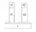
As shown in FIG. 1, a hard mask layer is deposited on a substrate template 1 comprising N-doped poly-silicon 31 and undoped poly-silicon 32 to form an N-doped poly-silicon hard mask layer 41 and an undoped poly-silicon hard mask layer 42, respectively, and the undoped poly-silicon hard mask layer 42 is etched so as to have a thickness less than that of the N-doped poly-silicon hard mask layer 41. The etching of the undoped poly-silicon hard mask layer 42 can be performed by using a patterned photoresist PR as a mask. The resulting structure is shown in FIG. 2.
As shown in FIG. 3, an anti-reflection layer 5 is deposited on the N-doped poly-silicon hard mask layer 41 and the undoped poly-silicon hard mask layer 42 which have different thicknesses. The formed device is etched according to a predetermined pattern until the N-doped poly-silicon 31 is exposed. As shown in FIG. 4, when the N-doped poly-silicon 31 is exposed, the undoped poly-silicon 32 is etched to a certain degree.
Afterwards, the residuals on the device surface during etching are removed. Then the device is etched to form an N-doped poly-silicon gate 41 and an undoped poly-silicon gate 42, as shown in FIG. 5.
In the step of etching to form the poly-silicon gates, there is a difference in etching rate between the N-doped poly-silicon 31 and the undoped poly-silicon 32. Therefore, it is necessary to determine the remaining thickness of the undoped poly-silicon to be etched when the etching of the N-doped poly-silicon gate is complete. The remaining thickness is determined according to the etching rate ratio of the undoped poly-silicon and N-doped poly-silicon. In an embodiment, the remaining thickness is calculated according to the following equation:
T Ppoly _ remain = T Poly - ER Ppoly _ poly ER Npoly _ poly × T poly ( 1 )
where TPpoly—remain is the remaining thickness of the undoped poly-silicon when the etching of the N-doped poly-silicon gate is complete in the conventional technology, Tpoly is the total thickness of the poly-silicon composed of the N-doped and undoped poly-silicon, ERPpoly—poly is the etching rate of the undoped poly-silicon, ERNpoly—poly is the etching rate of the N-doped poly-silicon.
Since the remaining thickness of the undoped poly-silicon equals to the thickness of the undoped poly-silicon TPpoly—etch which is required to be etched during the etching of the hard mask layers, then
TPpoly—etch=TPpoly—remain (2)
During the step of etching the hard mask layers, the etching thickness of the hard mask layer on the undoped poly-silicon, i.e., the thickness difference between the undoped poly-silicon hard mask layer and the N-doped poly-silicon hard mask layer THM—Ppoly, is determined according to the etching rate ratio of the hard mask layer and the undoped poly-silicon. In an embodiment, the thickness difference THM—Ppoly is calculated according to the following equation:
T HM _ P poly = ER HM _ HM ER Ppoly _ HM × T Ppoly _ etch ( 3 )
where ERHM—HM is the etching rate of the hard mask layer, and ERPpoly—HM is the etching rate of the undoped poly-silicon.
From the calculated thickness difference THM—Ppoly and the etching rate of the hard mask layer ERHM—HM, it is possible to calculate the etching time TimeHM—etch for the hard mask layer located on the undoped poly-silicon. The etching time TimeHM—etch is calculated according to the following equation:
Time HM _ etch = T HM _ Ppoly ER HM _ HM ( 4 )
The specific embodiments of the present invention have been described as above, but the present invention is not limited to the embodiments described above, since these embodiments are only exemplary in nature. It is apparent for the skilled in the art that any equivalent modification and substitution fall within the scope of the present invention. Therefore, all equivalent modifications and substitutions without departing from the spirit and scope of the present invention should be covered by the present invention.
Claims
1. A method for reducing the morphological difference between the N-doped and undoped poly-silicon gates after etching comprising the following sequential steps:
Step 1: depositing a hard mask layer on a substrate template having N-doped poly-silicon and undoped poly-silicon to form an N-doped poly-silicon hard mask layer and an undoped poly-silicon hard mask layer respectively, and etching the undoped poly-silicon hard mask layer to make a thickness difference between the N-doped poly-silicon hard mask layer and the undoped poly-silicon hard mask layer; the thickness of the undoped poly-silicon hard mask layer is etched to be less than that of the N-doped poly-silicon hard mask layer;
Step 2: depositing an anti-reflection layer on the N-doped poly-silicon hard mask layer and the undoped poly-silicon hard mask layer with different thicknesses, and etching according to a predetermined pattern until exposing the N-doped poly-silicon, wherein when the N-doped poly-silicon is exposed, the undoped poly-silicon is etched to a certain degree;
Step 3: removing residuals formed during etching on the surface of the above structure formed by Step 2, and etching the N-doped poly-silicon and undoped poly-silicon to form an N-doped poly-silicon gate and an undoped poly-silicon gate, respectively.
2. The method of claim 1, wherein the thickness difference between the undoped poly-silicon hard mask layer and the N-doped poly-silicon hard mask layer in the Step 1 is related to the etching rate ratio of the hard mask layer and the undoped poly-silicon in the Step 2, as well as the etching rate ratio of the undoped poly-silicon and N-doped poly-silicon in the Step 3.
3. The method of claim 2, wherein the thickness difference between the undoped poly-silicon hard mask layer and the N-doped poly-silicon hard mask layer in the Step 1 is calculated according to the following equation:
T HM _ P poly = ER HM _ HM ER Ppoly _ HM × T Ppoly _ etch
where THM—Ppoly is the thickness difference between the undoped poly-silicon hard mask layer and the N-doped poly-silicon hard mask layer in the Step 1,
ERHM—HM is the etching rate of the hard mask layer in the Step 2,
ERPpoly—HM is the etching rate of the undoped poly-silicon in the Step 2,
TPpoly—etch is the etching thickness of the undoped poly-silicon when the N-doped poly-silicon is exposed in the Step 2, and TPpoly—etch is calculated according to the following equation:
TPpoly—etch=TPpoly—remain
where TPpoly—remain is the remaining thickness of the undoped poly-silicon when the etching of the N-doped poly-silicon gate is complete in the conventional technology, and TPpoly—remain is calculated according to the following equation:
T Ppoly _ remain = T poly - ER Ppoly _ poly ER Npoly _ poly × T poly
where Tpoly is the total thickness of the N-doped and undoped poly-silicon,
ERPpoly—poly is the etching rate of the undoped poly-silicon,
ERNpoly—poly is the etching rate of the N-doped poly-silicon.
4. The method of claim 1, wherein the etching time for etching the undoped poly-silicon hard mask layer is calculated according to the following equation:
Time HM _ etch = T HM _ Ppoly ER HM _ HM
where TimeHM—etch is the etching time for etching the undoped poly-silicon hard mask layer in the Step 1,
ERHM—HM is the etching rate of the hard mask layer in the Step 1,
THM—Ppoly is the thickness difference between the undoped poly-silicon hard mask layer and the N-doped poly-silicon hard mask layer in the Step 1, and THM—Ppoly is calculated according to the following equation:
T HM _ P poly = ER HM _ HM ER Ppoly _ HM × T Ppoly _ etch
Where THM—Ppoly is the thickness difference between the undoped poly-silicon hard mask layer and the N-doped poly-silicon hard mask layer in the Step 1,
ERHM—HM is the etching rate of the hard mask layer in the Step 2,
ERPpoly—HM is the etching rate of the undoped poly-silicon in the Step 2,
TPpoly—etch is the etching thickness of the undoped poly-silicon when the N-doped poly-silicon is exposed in the Step 2, and TPpoly—etch is calculated according to the following equation:
TPpoly—etch=TPpoly—remain
where TPpoly—remain is the remaining thickness of the undoped poly-silicon when the etching of the N-doped poly-silicon gate is complete in the conventional technology, and TPpoly—remain is calculated according to the following equation:
T Ppoly _ remain = T poly - ER Ppoly _ poly ER Npoly _ poly × T poly
where Tpoly is the total thickness of the N-doped and undoped poly-silicon,
ERPpoly—poly is the etching rate of the undoped poly-silicon,
ERNpoly—poly is the etching rate of the N-doped poly-silicon.
Images & Drawings included:


Sources:
- United States Patent and Trademark Office - verify current appl. status at the USPTO↗
Recent applications in this class:
- » 20230360917 2023-11-09
SEMICONDUCTOR DEVICE AND METHOD FOR FABRICATING THE SAME - » 20190311904 2019-10-10
Array substrate, fabricating method thereof, and display device - » 20190057873 2019-02-21
Semiconductor device and power converter including a copper film with a small grain size stress relaxtion layer - » 20190006181 2019-01-03
Semiconductor device - » 20180240673 2018-08-23
Transistor, protection circuit, and method of manufacturing transistor - » 20180218910 2018-08-02
Semiconductor device with p-type AlxInyGal-x-yN and ohmic electrode thereof - » 20180190495 2018-07-05
Organic thin film transistor and method for manufacturing organic thin film transistor - » 20180061643 2018-03-01
METHOD FOR PRODUCING THIN FILM TRANSISTOR AND THIN FILM TRANSISTOR - » 20180040482 2018-02-08
Method of forming low height split gate memory cells - » 20180033629 2018-02-01
Integrated circuit element and fabricating method thereof, circuit board, display panel and display device
Recent applications for this Assignee:
- » 20250107251 2025-03-27
METHOD FOR MAKING IMAGE SENSOR - » 20250098338 2025-03-20
SILICON PHOTOMULTIPLIER TUBE - » 20250089259 2025-03-13
NON-VOLATILE MEMORY - » 20250080106 2025-03-06
System for turning off power consumption of auxiliary startup circuit - » 20250076195 2025-03-06
Method for Monitoring Ghost Image of Illumination Unit of Lithography Machine - » 20250075979 2025-03-06
FIXING APPARATUS FOR FURNACE WIRE OF FURNACE BODY HEATER - » 20250075976 2025-03-06
INJECTOR MOUNTING APPARATUS OF FURNACE - » 20250069955 2025-02-27
Method and System for Analyzing Wafer Angle in Semiconductor Integrated Circuit Manufacturing - » 20250069666 2025-02-27
One Time Programmable Memory Cell - » 20240186140 2024-06-06
Method for Forming Mixed Substrate