Adjustable avalanche diode in an integrated circuit
US20130328150A1
2013-12-12
13/895,715
2013-05-16
✅ Patent granted
US 9,018,729 B2
2015-04-28
-
-
Hoang-Quan Ho
Allen, Dyer, Doppelt, Milbrath & Gilchrist, P.A.
2033-05-16
Abstract:
An avalance diode including, between two heavily-doped regions of opposite conductivity types arranged at the surface of a semiconductor region, a lightly-doped region, with length L of the lightly-doped region between the heavily-doped regions approximately ranging between 50 and 200 nm.
Assignee:
- STMICROELECTRONICS SA 1,955 🇫🇷 Montrouge, France
- STMicroelectronics (CROLLES 2) SAS 863 🇫🇷 Crolles, France
- STMicroelectronics International NV 1 🇫🇷 Crolles, France
Applicant:
Interested in similar patents?
Get notified when new applications in this technology area are published.
Classification:
H01L31/1892 » CPC further
Semiconductor devices sensitive to infra-red radiation, light, electromagnetic radiation of shorter wavelength or corpuscular radiation and specially adapted either for the conversion of the energy of such radiation into electrical energy or for the control of electrical energy by such radiation; Processes or apparatus specially adapted for the manufacture or treatment thereof or of parts thereof; Details thereof; Processes or apparatus specially adapted for the manufacture or treatment of these devices or of parts thereof methods involving the use of temporary, removable substrates
H01L31/0256 » CPC main
Semiconductor devices sensitive to infra-red radiation, light, electromagnetic radiation of shorter wavelength or corpuscular radiation and specially adapted either for the conversion of the energy of such radiation into electrical energy or for the control of electrical energy by such radiation; Processes or apparatus specially adapted for the manufacture or treatment thereof or of parts thereof; Details thereof characterised by their semiconductor bodies characterised by the material
H01L29/866 » CPC further
Semiconductor devices adapted for rectifying, amplifying, oscillating or switching, or capacitors or resistors with at least one potential-jump barrier or surface barrier, e.g. PN junction depletion layer or carrier concentration layer; Details of semiconductor bodies or of electrodes thereof; Multistep manufacturing processes therefor; Types of semiconductor device ; Multistep manufacturing processes therefor controllable only by variation of the electric current supplied, or only the electric potential applied, to one or more of the electrodes carrying the current to be rectified, amplified, oscillated or switched; Diodes Zener diodes
H01L23/58 IPC
Details of semiconductor or other solid state devices Structural electrical arrangements for semiconductor devices not otherwise provided for, e.g. in combination with batteries
H01L29/66 IPC
Semiconductor devices adapted for rectifying, amplifying, oscillating or switching, or capacitors or resistors with at least one potential-jump barrier or surface barrier, e.g. PN junction depletion layer or carrier concentration layer; Details of semiconductor bodies or of electrodes thereof; Multistep manufacturing processes therefor Types of semiconductor device ; Multistep manufacturing processes therefor
H01L29/06 IPC
Semiconductor devices adapted for rectifying, amplifying, oscillating or switching, or capacitors or resistors with at least one potential-jump barrier or surface barrier, e.g. PN junction depletion layer or carrier concentration layer; Details of semiconductor bodies or of electrodes thereof; Multistep manufacturing processes therefor; Semiconductor bodies ; Multistep manufacturing processes therefor characterised by their shape; characterised by the shapes, relative sizes, or dispositions of the semiconductor regions ; characterised by the concentration or distribution of impurities within semiconductor regions
H01L29/0684 » CPC further
Semiconductor devices adapted for rectifying, amplifying, oscillating or switching, or capacitors or resistors with at least one potential-jump barrier or surface barrier, e.g. PN junction depletion layer or carrier concentration layer; Details of semiconductor bodies or of electrodes thereof; Multistep manufacturing processes therefor; Semiconductor bodies ; Multistep manufacturing processes therefor characterised by their shape; characterised by the shapes, relative sizes, or dispositions of the semiconductor regions ; characterised by the concentration or distribution of impurities within semiconductor regions characterised by the shape, relative sizes or dispositions of the semiconductor regions or junctions between the regions
H01L27/144 » CPC further
Devices consisting of a plurality of semiconductor or other solid-state components formed in or on a common substrate including semiconductor components sensitive to infra-red radiation, light, electromagnetic radiation of shorter wavelength or corpuscular radiation and specially adapted either for the conversion of the energy of such radiation into electrical energy or for the control of electrical energy by such radiation Devices controlled by radiation
H01L31/18 IPC
Semiconductor devices sensitive to infra-red radiation, light, electromagnetic radiation of shorter wavelength or corpuscular radiation and specially adapted either for the conversion of the energy of such radiation into electrical energy or for the control of electrical energy by such radiation; Processes or apparatus specially adapted for the manufacture or treatment thereof or of parts thereof; Details thereof Processes or apparatus specially adapted for the manufacture or treatment of these devices or of parts thereof
Description
CROSS REFERENCE TO RELATED APPLICATION
This application is a translation of and claims the priority benefit of French patent application number 12/55433, filed on Jun. 11, 2012, entitled: “ADJUSTABLE AVALANCHE DIODE IN AN INTEGRATED CIRCUIT,” which is hereby incorporated by reference to the maximum extent allowable by law.
BACKGROUND
1. Technical Field
The present disclosure relates to the field of avalanche diodes, which are especially used as protection diodes in integrated circuits.
2. Discussion of the Art
One of the current ways of obtaining a determined reference voltage or breakdown voltage in an integrated circuit consists in using a reverse-biased PN junction. The breakdown voltage or avalanche voltage is then essentially set by the doping level of the less heavily doped region. For the PR junction, and especially for the less heavily doped region, it is desired to use a region having a doing level existing in the manufacturing technology of the integrated circuit where this PN junction is to be inserted, to avoid having to use a specific technological step to manufacture the avalanche diode. It is thus not always possible to directly obtain the desired breakdown voltage.
The same issue arises all the more when several avalanche diodes are desired to be formed in an integrated circuit, such avalanche diodes having different determined breakdown voltages. The number of breakdown voltages which can be obtained is rather limited and such voltages are predetermined by the doping levels existing in the various integrated circuit manufacturing blocks.
There thus is a need, especially in the field of integrated circuits, for avalanche diodes having adjustable avalanche voltages without requiring the use of specific doping levels or of complex structures.
BRIEF SUMMARY
Thus, an embodiment provides an avalanche diode comprising, between two heavily-doped regions of opposite conductivity types arranged at the surface of a semiconductor region, a lightly-doped region, with length L of the lightly-doped region between the heavily-doped regions approximately ranging between 50 and 200 nm.
According to an embodiment, the lightly-doped region has a doping level ranging between 1014 and 1016 atoms/cm3.
An embodiment provides an integrated circuit comprising several avalanche diodes such as hereabove, having different lengths L.
An embodiment provides a method for adjusting the breakdown voltage of an avalanche diode of the above type, comprising selecting by masking the distance between the two heavily-doped regions.
The foregoing and other features and benefits will be discussed in detail in the following non-limiting description of specific embodiments in connection with the accompanying drawings.
BRIEF DESCRIPTION OF THE DRAWINGS
FIG. 1 is a simplified cross-section view of an embodiment of an adjustable avalanche diode; and
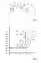
FIG. 2 shows various avalanche characteristics obtained with diodes of the type shown in FIG. 1.
As usual in the representation of integrated circuits, FIG. 1 is not to scale.
DETAILED DESCRIPTION
FIG. 1 shows an avalanche diode comprising, in a region of a semiconductor substrate 1 preferably delimited by an insulating ring 3, respective heavily doped N-type regions and P-type regions 5 and 6 separated by a portion 7 of the substrate . Cathode contact K and anode contact A on regions 5 and 6 of the diode are taken in any conventional manner, for example, via metal suicide regions 8 and 9.
Call L the length of lightly-doped region 7 between the opposite limits of heavily-doped regions 5 and 6.
The inventors have noted that, when length L becomes smaller than approximately 250 nm, the diode has a breakdown voltage which essentially depends on length L and no longer essentially on the doping level of the less heavily doped region (the substrate).
Curves 11 to 15 of FIG. 2 show current versus reverse voltage characteristics for such a diode in the case where the substrate doping is on the order of 1015 at./cm3. For respective values of length L of 0.12, 0.14, 0.16, 0.18, and 0.20 μm, the breakdown voltage varies between approximately 6 and approximately 9 volts. It should be noted that the avalanche knee point is strongly marked and the current-vs.-voltage characteristics become substantially vertical as soon as the current in the diode exceeds a value ranging between 10−7 and 10−9 amperes. In other words, the avalanche diode has a very small reverse-mode current leakage below the avalanche threshold.
However, if the substrate is more heavily doped, for example, if P substrate 1 is formed by a well such as currently used in integrated circuits, with a doping level approximately ranging between 1017 and 1018 at./cm3, the same type of characteristics will be obtained with, however, a much more rounded knee point, as indicated by curve 21 for a 0.16-μm length L.
Thus, if an avalanche diode with little reverse-mode leakage is desired to be formed, it is desirable to use a lightly-doped substrate, preferably, having a doping level ranging between 1014 and 1016 at./cm3.
It should be noted that the adjustment of the breakdown voltage of a diode such as described hereabove is particularly easy to obtain. Instead of resulting from technological diffusion and implantation operations aiming at obtaining specific doping levels, this adjustment only results from the shape of the mask(s) used to form the various regions, and especially regions 5 and 6 of FIG. 1 at a selected distance L from each other. According to this distance L, different breakdown voltages will be obtained.
Although N+ and P+ regions separated by a lightly-doped P-type substrate region have been described herein, this substrate region may be lightly N-type doped.
Such alterations, modifications, and improvements are intended to be part of this disclosure, and are intended to be within the spirit and the scope of the present invention. Accordingly, the foregoing description is by way of example only and is not intended to be limiting. The present invention is limited only as defined in the following claims and the equivalents thereto.
Claims
What is claimed is:1. An avalanche diode comprising, between two heavily-doped regions of opposite conductivity types arranged at the surface of a semiconductor region, a lightly-doped region, with length L of the lightly-doped region between the heavily-doped regions approximately ranging between 50 and 200 nm. said lightly-doped region not being covered by a gate.
2. The avalanche diode of claim 1, wherein the lightly-doped region has a doping level ranging between 1014 and 1016 atoms/cm3.
3. An integrated circuit comprising several avalanche diodes of claim 1 of different lengths L.
4. A method for adjusting the breakdown voltage of the avalanche diode of claim 1, comprising selecting by masking the distance between the two heavily-doped regions.
Images & Drawings included:

Sources:
- United States Patent and Trademark Office - verify current appl. status at the USPTO↗
Recent applications in this class:
- » 20240178331 2024-05-30
Light Receiving Device - » 20220320354 2022-10-06
Graphene-containing membrane, process for producing the same, graphene-containing membrane laminate and photoelectric conversion device - » 20220085221 2022-03-17
Evaluation method on anion permeability of graphene-containing membrane and photoelectric conversion device - » 20200395491 2020-12-17
Graphene-containing membrane, process for producing the same, graphene-containing membrane laminate and photoelectric conversion device - » 20200212231 2020-07-02
Evaluation method on anion permeability of graphene-containing membrane and photoelectric conversion device - » 20200119206 2020-04-16
Perovskite solar cell - » 20190393364 2019-12-26
ORGANIC SOLAR CELL - » 20180212074 2018-07-26
Polymer containing 1,2,5-benzoselenadiazole-N-R1-5,6-dicarboxylic acid imide and preparation method and use thereof - » 20180175219 2018-06-21
Organic solar cell and manufacturing method therefor - » 20180138326 2018-05-17
ORGANIC THIN FILM SOLAR CELL MODULE, ELECTRONIC DEVICE AND METHOD FOR MANUFACTURING ORGANIC THIN FILM SOLAR CELL MODULE
Recent applications for this Assignee:
- » 20250275172 2025-08-28
SEMICONDUCTOR INTEGRATED CIRCUIT COMPONENT - » 20250210550 2025-06-26
ELECTRONIC CIRCUIT COMPRISING A RF SWITCHES HAVING REDUCED PARASITIC CAPACITANCES - » 20250204075 2025-06-19
PIXEL OF A LIGHT SENSOR AND METHOD FOR MANUFACTURING SAME - » 20250185390 2025-06-05
LIGHT SENSOR PIXEL AND METHOD OF MANUFACTURING THE SAME - » 20250174489 2025-05-29
FORMING OF TRENCHES IN A SUBSTRATE - » 20250164680 2025-05-22
OPTICAL DEVICE - » 20250160032 2025-05-15
IMAGE SENSOR PIXELS HAVING REDUCED PITCH - » 20250126877 2025-04-17
SEMICONDUCTOR CHIP MANUFACTURING METHOD - » 20250039577 2025-01-30
PIXEL WITH GLOBAL SHUTTER - » 20240405146 2024-12-05
SPAD PHOTODIODE