Structure and method for bump to landing trace ratio
US20140131865A1
2014-05-15
14/168,800
2014-01-30
✅ Patent granted
US 8,981,576 B2
2015-03-17
-
-
S. V. Clark
Haynes and Boone, LLP
2034-01-30
Abstract:
The present disclosure provides an integrated circuit. The integrated circuit includes an interconnect structure formed on a substrate; a landing metal trace formed on the interconnect structure and coupled to the interconnect structure, wherein the landing metal trace includes a first width T defined in a first direction; and a metal bump post formed on and aligned with the landing metal trace, wherein the metal bump post includes a second width U defined in the first direction, and the second width U is greater than the first width T.
Inventors:
- Tin-Hao KUO 108 🇹🇼 Hsinchu City, Taiwan
- Chen-Shien Chen 319 🇹🇼 Zhubei City, Taiwan
- Mirng-Ji Lii 177 🇹🇼 Sinpu Township, Taiwan
- Chen-Hua Yu 522 🇹🇼 Hsinchu City, Taiwan
- Sheng-Yu Wu 16 🇹🇼 Hsinchu City, Taiwan
- Yen-Liang Lin 71 🇹🇼 Taichung City, Taiwan
- Chen-Hua YU 1,372 🇹🇼 Hsinchu, Taiwan
- Yen-Liang Lin 66 🇹🇼 Taichung, Taiwan
- Chen-Shien Chen 311 🇹🇼 Zhubei, Taiwan
- Tin-Hao Kuo 189 🇹🇼 Hsinchu, Taiwan
- Sheng-Yu Wu 28 🇹🇼 Hsinchu, Taiwan
Assignee:
- TAIWAN SEMICONDUCTOR MANUFACTURING COMPANY, LTD. 8,890 🇹🇼 Hsin-Chu, Taiwan
Applicant:
Interested in similar patents?
Get notified when new applications in this technology area are published.
Classification:
H01L23/49811 » CPC main
Details of semiconductor or other solid state devices; Arrangements for conducting electric current to or from the solid state body in operation, e.g. leads, terminal arrangements ; Selection of materials therefor consisting of soldered constructions; Leads, on insulating substrates, Additional leads joined to the metallisation on the insulating substrate, e.g. pins, bumps, wires, flat leads
H01L24/13 » CPC further
Arrangements for connecting or disconnecting semiconductor or solid-state bodies; Methods or apparatus related thereto; Means for bonding being attached to, or being formed on, the surface to be connected, e.g. chip-to-package, die-attach, "first-level" interconnects; Manufacturing methods related thereto; Bump connectors ; Manufacturing methods related thereto; Structure, shape, material or disposition of the bump connectors prior to the connecting process of an individual bump connector
H01L24/16 » CPC further
Arrangements for connecting or disconnecting semiconductor or solid-state bodies; Methods or apparatus related thereto; Means for bonding being attached to, or being formed on, the surface to be connected, e.g. chip-to-package, die-attach, "first-level" interconnects; Manufacturing methods related thereto; Bump connectors ; Manufacturing methods related thereto; Structure, shape, material or disposition of the bump connectors after the connecting process of an individual bump connector
H01L2224/13005 » CPC further
Indexing scheme for arrangements for connecting or disconnecting semiconductor or solid-state bodies and methods related thereto as covered by; Means for bonding being attached to, or being formed on, the surface to be connected, e.g. chip-to-package, die-attach, "first-level" interconnects; Manufacturing methods related thereto; Bump connectors; Manufacturing methods related thereto; Structure, shape, material or disposition of the bump connectors prior to the connecting process of an individual bump connector; Core members of the bump connector Structure
H01L23/49816 » CPC further
Details of semiconductor or other solid state devices; Arrangements for conducting electric current to or from the solid state body in operation, e.g. leads, terminal arrangements ; Selection of materials therefor consisting of soldered constructions; Leads, on insulating substrates,; Additional leads joined to the metallisation on the insulating substrate, e.g. pins, bumps, wires, flat leads Spherical bumps on the substrate for external connection, e.g. ball grid arrays [BGA]
H01L23/498 IPC
Details of semiconductor or other solid state devices; Arrangements for conducting electric current to or from the solid state body in operation, e.g. leads, terminal arrangements ; Selection of materials therefor consisting of soldered constructions Leads, on insulating substrates,
H01L2224/1145 » CPC further
Indexing scheme for arrangements for connecting or disconnecting semiconductor or solid-state bodies and methods related thereto as covered by; Means for bonding being attached to, or being formed on, the surface to be connected, e.g. chip-to-package, die-attach, "first-level" interconnects; Manufacturing methods related thereto; Bump connectors; Manufacturing methods related thereto; Manufacturing methods by blanket deposition of the material of the bump connector in gaseous form Physical vapour deposition [PVD], e.g. evaporation, or sputtering
H01L2224/1146 » CPC further
Indexing scheme for arrangements for connecting or disconnecting semiconductor or solid-state bodies and methods related thereto as covered by; Means for bonding being attached to, or being formed on, the surface to be connected, e.g. chip-to-package, die-attach, "first-level" interconnects; Manufacturing methods related thereto; Bump connectors; Manufacturing methods related thereto; Manufacturing methods by blanket deposition of the material of the bump connector Plating
H01L21/76885 » CPC further
Processes or apparatus adapted for the manufacture or treatment of semiconductor or solid state devices or of parts thereof; Manufacture or treatment of devices consisting of a plurality of solid state components formed in or on a common substrate or of parts thereof; Manufacture of integrated circuit devices or of parts thereof; Manufacture of specific parts of devices defined in group; Applying interconnections to be used for carrying current between separate components within a device comprising conductors and dielectrics characterised by the formation and the after-treatment of the conductors By forming conductive members before deposition of protective insulating material, e.g. pillars, studs
H01L2924/1306 » CPC further
Indexing scheme for arrangements or methods for connecting or disconnecting semiconductor or solid-state bodies as covered by; Details of semiconductor or other solid state devices to be connected; Device type; Discrete devices, e.g. 3 terminal devices; Transistor Field-effect transistor [FET]
H01L23/48 IPC
Details of semiconductor or other solid state devices Arrangements for conducting electric current to or from the solid state body in operation, e.g. leads, terminal arrangements ; Selection of materials therefor
H01L23/52 IPC
Details of semiconductor or other solid state devices Arrangements for conducting electric current within the device in operation from one component to another, i.e. interconnections, e.g. wires, lead frames
H01L29/40 IPC
Semiconductor devices adapted for rectifying, amplifying, oscillating or switching, or capacitors or resistors with at least one potential-jump barrier or surface barrier, e.g. PN junction depletion layer or carrier concentration layer; Details of semiconductor bodies or of electrodes thereof; Multistep manufacturing processes therefor Electrodes ; Multistep manufacturing processes therefor
H01L23/00 IPC
Details of semiconductor or other solid state devices
H01L21/768 IPC
Processes or apparatus adapted for the manufacture or treatment of semiconductor or solid state devices or of parts thereof; Manufacture or treatment of devices consisting of a plurality of solid state components formed in or on a common substrate or of parts thereof; Manufacture of integrated circuit devices or of parts thereof; Manufacture of specific parts of devices defined in group Applying interconnections to be used for carrying current between separate components within a device comprising conductors and dielectrics
Description
This application is a continuation application of U.S. patent application Ser. No. 13/426,386, filed Mar. 21, 2012, which claims the benefit of U.S. Provisional Patent Application Ser. No. 61/512,283 entitled “Structure and Method For Bump To Landing Trace Ratio,” filed Jul. 27, 2011, each of which is hereby incorporated by reference in its entirety.
BACKGROUND
In advanced integrated circuit technology, device dimensions are scaled down. Various factors degrade the performance of the integrated circuit. The electro-migration (EM) issue is impacted by the structure and dimensions of under bump metal (UBM) in the backend of line. On the other side, changing the structure and dimensions of the UBM intended to improve EM performance may cause other issue, such as bump to bride bridging. The bump fatigue performance is degraded. Therefore, a structure of an UBM and the method making the same are needed to address the above issue.
BRIEF DESCRIPTION OF THE DRAWINGS
Aspects of the present disclosure are best understood from the following detailed description when read with the accompanying figures. It is emphasized that, in accordance with the standard practice in the industry, various features are not drawn to scale. In fact, the dimensions of the various features may be arbitrarily increased or reduced for clarity of discussion.
FIG. 1 illustrates a sectional view of a bonding structure of an integrated circuit constructed according to various aspects of the present disclosure in one or more embodiments.
FIG. 2 illustrates a perspective view of the integrated circuit of FIG. 1 according one or more embodiments.
FIG. 3 illustrates a sectional view of a bonding structure of an integrated circuit constructed according to various aspects of the present disclosure in one or more embodiments.
FIG. 4 illustrates a top view of the integrated circuit of FIG. 3 according one or more embodiments.
FIG. 5 illustrates perspective views of the metal bump post according to various embodiments.
FIG. 6 illustrates top views of the metal bump post according to various embodiments.
DETAILED DESCRIPTION
It is to be understood that the following disclosure provides many different embodiments, or examples, for implementing different features of various embodiments. Specific examples of components and arrangements are described below to simplify the present disclosure. These are, of course, merely examples and are not intended to be limiting. In addition, the present disclosure may repeat reference numerals and/or letters in the various examples. This repetition is for the purpose of simplicity and clarity and does not in itself dictate a relationship between the various embodiments and/or configurations discussed. Moreover, the formation of a first feature over or on a second feature in the description that follows may include embodiments in which the first and second features are formed in direct contact, and may also include embodiments in which additional features may be formed interposing the first and second features, such that the first and second features may not be in direct contact.
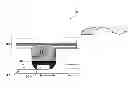
FIG. 1 illustrates a sectional view of a bonding structure of an integrated circuit 10 constructed according to various aspects of the present disclosure in one or more embodiments. FIG. 2 illustrates a perspective view of the integrated circuit 10 according one or more embodiments. The integrated circuit 10 and the method of making the same are collectively described with reference to FIGS. 1 and 2.
The integrated circuit 10 is formed on a semiconductor substrate (not shown), such as a silicon substrate. Alternatively or additionally, the substrate includes germanium, silicon germanium or other proper semiconductor materials. The semiconductor substrate may also include various isolation features, such as shallow trench isolation (STI), formed in the substrate to separate various devices. The semiconductor substrate also includes various doped regions such as n-well and p-wells.
The integrate circuit 10 further include various devices, such as transistors, diodes, resistors, capacitors, sensors, memory cells or other suitable IC devices. In one example, the integrated circuit 10 includes field effect transistor having source and drain features formed in the semiconductor substrate and further includes a gate stack formed on the semiconductor substrate and disposed between the source and drain features configured to form a functional transistor.
The integrated circuit 10 also include an interconnect structure having various metal layers. The interconnect structure includes metal lines formed in the metal layers and contact features and via features. The contact features connect the doped features and/or gate electrodes to respective metal lines and the via features connect metal lines in neighboring metal layers. The interconnect structure is configured to couple the various doped features and conductive features to form various devices, resulting in one or more functional circuits integrated on the semiconductor substrate.
Particularly, the integrated circuit 10 includes various bonding structures to couple the various IC devices to the packaging (or packaging substrate) and further to the input/output signals and power sources. In one example, features 45 is a portion of the substrate with devices and the interconnect structure and the features 42 is a portion of the packaging substrate.
FIG. 1 only shows one bonding structure for simplicity. The bonding structure includes a landing metal trace 20 properly coupled to the interconnect structure and further includes a metal bump post (or metal post) 40 aligned with and overlying the landing metal trace 20. In one embodiment, various conductive features may be disposed between the landing metal trace 20 and the metal bump post 40. In this embodiment, a ratio T/U is below 0.6.
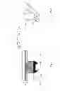
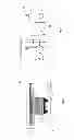
FIG. 3 illustrates a sectional view of a bonding structure of an integrated circuit 50 constructed according to various aspects of the present disclosure in one or more embodiments. FIG. 4 illustrates a top view of the integrated circuit 50 according one or more embodiments. The integrated circuit 50 and the method of making the same are collectively described with reference to FIGS. 3 and 4. The integrated circuit 50 is also formed on a substrate, such as a semiconductor substrate. The integrated circuit 50 also includes various devices and an interconnect structure.
The integrated circuit 50 includes various bonding structures to couple the various IC devices to the packaging and further to the input/output signals and power sources. FIG. 3 only illustrates one bonding structure for simplicity. The bonding structure includes a landing metal trace 20 properly coupled to the interconnect structure and further includes a metal bump post 40 aligned with, overlying and coupled with the landing metal trace 20. In one example, the metal bump post 40 includes copper formed by sputtering, plating or combination.
The landing metal trace 20 defines a width labeled as “T” in FIG. 4. The width T is defined and spanned in a direction perpendicular to the direction of an electrical current through the landing metal trace 20. The metal bump post 40 defines a width labeled as “U” and a length labeled as “L” in FIG. 4. The width U is defined as a dimension perpendicular to the landing metal trace routing direction. A space “S” is defined between a metal bump post and a proximate landing metal trace, as illustrated in FIGS. 3 and 4. The length L is defined to be spanned in a first direction of the electrical current. The widths U and T are defined to be spanned in a second direction perpendicular to the first direction. Particularly, according to the present embodiment, the width U of the metal bump post 20 is greater than the width T of the landing metal trace 20.
In furtherance of the embodiment, the ratio L/U is less than 2 as L/U<2. The ratio T/U ranges as 0.5=<T/U<1. Alternatively, the ratio T/U ranges as 0.7=<T/U<0.9, or 0.75=<T/U<0.85. The ratio S/T ranges as S/T<0.6. Alternatively, the ratio S/T ranges as S/T<0.5, or S/T<0.4. The ratio U/S ranges as 2<U/S<4. Alternatively, the ratio U/S ranges as 2.5<U/S<3.5.
The design consideration to the disclosure structure is based on the issues identified in the present disclosure. One issue the bridge risk that may occur at the interface between the landing metal trace 20 and the metal bump post 40. Another issue the electro-migration (EM). In the design consideration, the mean time between failures (MTTF) is determined by an equation formulated as MTTF=A(1/fn)×exp(Q/kT). The integrated circuit 50 effectively eliminates or reduces the bridge risk. The integrated circuit 50 further reduces the EM issue and enhances the circuit performance.
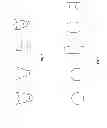
FIG. 5 illustrates perspective views of metal bump post 40 that may be incorporated in the integrated circuit 50 of FIGS. 3 and 4 according to various embodiments. The metal bump post 40 may have column shape, conical shape or other suitable shape, such as those shapes illustrated in FIG. 5.
FIG. 6 illustrates top views of the metal bump post 40 that may be incorporated in the integrated circuit 50 of FIGS. 3 and 4 according to various embodiments. The metal bump post 40 may have different geometries, such as round, polygon, elongated shape, oval shape or other suitable shape illustrated in FIG. 6.
Although embodiments of the present disclosure have been described in detail, those skilled in the art should understand that they may make various changes, substitutions and alterations herein without departing from the spirit and scope of the present disclosure. For example, the present disclosure is not limited to a particular application. In one example, the integrated circuit 50 may include various IC structure, such as a field effect transistor, a dynamic random access second (DRAM) cell, field programmable gate-array (FPGA) and/or other microelectronic devices. Of course, aspects of the present disclosure may be employed in many different applications, including sensor cells, logic cells, and others.
Thus, the present disclosure provides one embodiment of an integrated circuit. The integrated circuit includes an interconnect structure formed on a substrate; a landing metal trace formed on the interconnect structure and coupled to the interconnect structure, wherein the landing metal trace includes a first width T defined in a first direction; and a metal bump post formed on and aligned with the landing metal trace, wherein the metal bump post includes a second width U defined in the first direction, and the second width U is greater than the first width T.
In one embodiment of the integrated circuit, the first width T and the second width U define a first ratio T/U greater or equal to 0.5 and less than 1. In another embodiment, the first ratio T/U is greater or equal to 0.7 and less than 0.9. In yet another embodiment, the first ratio T/U is greater or equal to 0.75 and less than 0.85.
In another embodiment, the metal bump post includes a length defined in a second direction perpendicular to the first direction, a second ratio L/U is less than 2.
In yet another embodiment, the integrated circuit further includes a neighboring landing metal trace approximate to the landing metal trace, wherein a space S is defined as a distance between the metal bump post and the neighboring landing metal trace, and a third ratio S/T is less than 0.6.
In yet another embodiment, the third ratio S/T is less than 0.5. In yet another embodiment, the third ratio S/T is less than 0.4. In yet another embodiment, a fourth ratio U/S is greater than 2 and less than 4. In yet another embodiment, the fourth ratio U/S is greater than 2.5 and less than 3.5.
In yet another embodiment, the metal bump post includes copper. In yet another embodiment, the first direction is perpendicular to a direction of electrical current through the landing metal trace.
In yet another embodiment, the metal bump post includes a shape from one of column shape and conical shape.
In yet another embodiment, the metal bump post includes a shape, in top view, selected from the group consisting of round, polygon, elongated shape and oval shape.
The present disclosure also provides one embodiment of a method. The method includes forming an interconnect structure on a substrate; forming a landing metal trace on the interconnect structure, wherein the landing metal trace includes a first width T defined in a first direction; and forming a metal bump post on the landing metal trace, wherein the metal bump post includes a second width U defined in the first direction, and the second width U is greater than the first width T.
In one embodiment of the method, the forming of the metal bump post includes forming a copper post by at least one of deposition and plating.
In another embodiment, the method further includes forming various integrated circuit devices on the substrate.
In yet another embodiment, the forming of the metal bump post includes forming the metal bump post with a first ratio T/U greater or equal to 0.5 and less than 1.
In yet another embodiment, the forming of metal bump post includes forming the metal bump post with a shape selected from one of column shape and conical shape.
In yet another embodiment, the forming of the metal bump post includes forming the metal bump post with a shape, in top view, selected from the group consisting of round, polygon, elongated shape and oval shape.
The foregoing has outlined features of several embodiments. Those skilled in the art should appreciate that they may readily use the present disclosure as a basis for designing or modifying other processes and structures for carrying out the same purposes and/or achieving the same advantages of the embodiments introduced herein. Those skilled in the art should also realize that such equivalent constructions do not depart from the spirit and scope of the present disclosure, and that they may make various changes, substitutions and alterations herein without departing from the spirit and scope of the present disclosure.
Claims
1-20. (canceled)
21. A device comprising:
a landing metal trace formed on a substrate, wherein the landing metal trace includes a first width T defined in a first direction;
an interconnect structure disposed over the landing metal trace; and
a metal bump post disposed on the landing metal trace and coupled to the interconnect structure, wherein the metal bump post includes a second width U defined in the first direction, wherein the first width T and the second width U define a ratio T/U greater or equal to 0.5 and less than 1.
22. The device of claim 21, wherein the metal bump post includes a length defined in a second direction perpendicular to the first direction, and a ratio L/U is less than 2.
23. The device of claim 21, wherein the ratio T/U is greater or equal to 0.7 and less than 0.9.
24. The device of claim of claim 21, further comprising another landing metal trace approximate to the landing metal trace, wherein a space S is defined as a distance between the metal bump post and the another landing metal trace, and wherein a ratio S/T is less than 0.6.
25. The device of claim 24, wherein the ratio S/T is less than 0.5.
26. The device of claim 24, wherein the ratio S/T is less than 0.4.
27. The device of claim 24, wherein a ratio U/S is greater than 2 and less than 4.
28. The device of claim 24, wherein a ratio U/S is greater than 2.5 and less than 3.5.
29. A device comprising:
a landing conductive trace disposed on a substrate and coupled to an interconnect structure, wherein the landing conductive trace includes a first width T defined in a first direction; and
a conductive bump post disposed over and coupled to the landing conductive trace, wherein the conductive bump post includes a second width U defined in the first direction, and the second width U is greater than the first width T, wherein the conductive bump post includes a length defined in a second direction perpendicular to the first direction, and a ratio L/U is less than 2.
30. The device of claim 32, wherein the first width T and the second width U define a ratio T/U greater or equal to 0.5 and less than 1.
31. The device of claim 33, wherein the ratio T/U is greater or equal to 0.75 and less than 0.85.
32. The device of claim 33, further comprising another landing conductive trace approximate to the landing conductive trace, wherein a space S is defined as a distance between the conductive bump post and the another landing conductive trace, and wherein a ratio S/T is less than 0.6.
33. The device of claim 21, wherein the landing conductive trace is a landing metal trace.
34. The device of claim 21, wherein the conductive bump post includes copper.
35. A method comprising:
forming a landing metal trace on a substrate, wherein the landing metal trace includes a first width T defined in a first direction;
coupling a metal bump post to the landing metal trace, wherein the metal bump post includes a second width U defined in the first direction, and the second width U is greater than the first width T, wherein the first width T and the second width U define a ratio T/U greater or equal to 0.5 and less than 1.
36. The method of claim 35, further comprising forming the metal bump post on an interconnect structure, wherein after the coupling of the metal bump post to the landing metal trace the interconnect structure is coupled to the landing metal trace via the metal bump post.
37. The method of claim 36, wherein forming the metal bump post on the interconnect structure includes performing a copper deposition process.
38. The method of claim 35, wherein the metal bump post includes a length defined in a second direction perpendicular to the first direction, and a ratio L/U is less than 2.
39. The method of claim 35, further comprising forming another landing metal trace on the substrate approximate to the landing metal trace, wherein a space S is defined as a distance between the metal bump post and the another landing metal trace, and wherein a ratio S/T is less than 0.6.
40. The method of claim 39, wherein a ratio U/S is greater than 2 and less than 4.
Images & Drawings included:
Sources:
- United States Patent and Trademark Office - verify current appl. status at the USPTO↗
Similar patent applications:
- » 20130026614
Structure and method for bump to landing trace ratio
Recent applications in this class:
- » 20250293129 2025-09-18
SUBSTRATE UNIT - » 20250285950 2025-09-11
SEMICONDUCTOR DEVICE PACKAGE - » 20250273548 2025-08-28
PACKAGE COMPRISING A BRIDGE WITH SPRING PADS - » 20250253220 2025-08-07
POWER SEMICONDUCTOR MODULE ARRANGEMENT - » 20250253219 2025-08-07
PRESS-FIT TERMINAL AND SEMICONDUCTOR DEVICE - » 20250253218 2025-08-07
SEMICONDUCTOR PACKAGE AND MANUFACTURING METHOD OF SEMICONDUCTOR PACKAGE - » 20250253217 2025-08-07
PACKAGE COMPRISING SUBSTRATES WITH POST INTERCONNECTS - » 20250246526 2025-07-31
SEMICONDUCTOR MODULE - » 20250226299 2025-07-10
SEMICONDUCTOR PACKAGE AND METHOD FOR FABRICATING THE SAME - » 20250218912 2025-07-03
POLYMER HYBRID BONDING FOR COMPOSITE PACKAGES AND METHODS OF FORMING THE SAME
Recent applications for this Assignee:
- » 20240266341 2024-08-08
HYBRID BONDING WITH UNIFORM PATTERN DENSITY - » 20240224489 2024-07-04
SEMICONDUCTOR DEVICE - » 20240170063 2024-05-23
CONTENT ADDRESSABLE MEMORY ARRAY DEVICE STRUCTURE - » 20240161819 2024-05-16
MEMORY DEVICE AND MANUFACTURING THEREOF - » 20240153896 2024-05-09
SEMICONDUCTOR PACKAGE SYSTEM AND METHOD - » 20240120409 2024-04-11
Method for non-resist nanolithography - » 20240113080 2024-04-04
Semiconductor Device with Discrete Blocks - » 20240105632 2024-03-28
Method for forming a semiconductor device including forming a first interconnect structure on one side of a substrate having first metal feature closer the substrate than second metal feature and forming first and second tsv on other side of substrate connecting to the metal features - » 20240096816 2024-03-21
Method of manufacture overlay mark using laser marking process for semiconductor device - » 20240096383 2024-03-21
MEMORY DEVICE