Gridded antenna and method for manufacturing the same
US20140159962A1
2014-06-12
13/921,338
2013-06-19
✅ Patent granted
US 9,362,623 B2
2016-06-07
-
-
Trinh Dinh
Anova Law Group, PLLC
2034-04-29
Abstract:
An antenna is disclosed. The antenna includes a substrate and an antenna layer disposed on a top surface of the substrate. The antenna layer includes a patch and a feed line electrically connected to the patch. The patch includes a number of slots disposed at a center portion thereof for forming a gridding part and an edge part surrounding the gridding part. A ratio of the width of the edge part and the width of the patch is at least 0.32.
Inventors:
- Ng Guan Hong 11 🇸🇬 Singapore, Singapore
- Roger Tay 4 🇸🇬 Singapore, Singapore
- Yew Choon Tan 1 🇸🇬 Singapore, Singapore
Assignee:
- AAC TECHNOLOGIES PTE. LTD 958 🇸🇬 Singapore, Singapore
Applicant:
Interested in similar patents?
Get notified when new applications in this technology area are published.
Classification:
H01Q1/38 » CPC main
Details of, or arrangements associated with, antennas; Structural form of radiating elements, e.g. cone, spiral, umbrella; Particular materials used therewith formed by a conductive layer on an insulating support
H01Q9/0407 » CPC main
Electrically-short antennas having dimensions not more than twice the operating wavelength and consisting of conductive active radiating elements; Resonant antennas Substantially flat resonant element parallel to ground plane, e.g. patch antenna
H01Q1/2225 » CPC further
Details of, or arrangements associated with, antennas; Supports; Mounting means by structural association with other equipment or articles associated with components used in interrogation type services, i.e. in systems for information exchange between an interrogator/reader and a tag/transponder, e.g. in Radio Frequency Identification [RFID] systems used in active tags, i.e. provided with its own power source or in passive tags, i.e. deriving power from RF signal
H01Q9/0421 » CPC further
Electrically-short antennas having dimensions not more than twice the operating wavelength and consisting of conductive active radiating elements; Resonant antennas; Substantially flat resonant element parallel to ground plane, e.g. patch antenna with a shorting wall or a shorting pin at one end of the element
Y10T29/49016 » CPC further
Metal working; Method of mechanical manufacture; Electrical device making Antenna or wave energy "plumbing" making
H01Q1/24 IPC
Details of, or arrangements associated with, antennas; Supports; Mounting means by structural association with other equipment or articles with receiving set
H01Q9/04 IPC
Electrically-short antennas having dimensions not more than twice the operating wavelength and consisting of conductive active radiating elements Resonant antennas
H01Q1/22 IPC
Details of, or arrangements associated with, antennas; Supports; Mounting means by structural association with other equipment or articles
Description
FIELD OF THE INVENTION
The present disclosure relates to antennas for portable devices, and more specifically to a gridded antenna and a method for manufacturing the same.
DESCRIPTION OF RELATED ART
With the rapidly development of radio frequency identification technologies, radio frequency identification (RFID) tags are widely used in various fields such as distribution, logistic, material handling industries, and non-contact integrated circuits. A related radio frequency identification tag generally includes an antenna.
With the demands for low cost, reliable and flexible antenna for wireless communication, there is a growth in using conductive ink printed antenna. Conductive ink, being able to print on a variety of substrate materials such as polyester provides a promising alternative for printing antenna. However, the conductive ink, such as silver, is relatively expensive.
Therefore, it is desirable to provide a new antenna and a new method which can overcome the above-mentioned problems.
BRIEF DESCRIPTION OF THE DRAWINGS
Many aspects of the embodiments can be better understood with reference to the following drawings. The components in the drawings are not necessarily drawn to scale, the emphasis instead being placed upon clearly illustrating the principles of the present disclosure. Moreover, in the drawings, like reference numerals designate corresponding parts throughout the several views.
FIG. 1 shows a first conventional antenna related to the present disclosure;
FIG. 2 shows a gridded antenna in accordance with a first embodiment of the present disclosure;
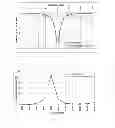
FIG. 3 illustrates a comparison of the return loss between the first conventional antenna and the gridded antenna;
FIG. 4 illustrates a comparison of the antenna efficiency between the first conventional antenna and the gridded antenna;
FIG. 5 shows a second conventional antenna related to the present disclosure;
FIG. 6 shows a gridded antenna in accordance with a second embodiment of the present disclosure;
FIG. 7 illustrates a comparison of the return loss between the second conventional antenna and the gridded antenna;
FIG. 8 illustrates a comparison of the antenna efficiency between the second conventional antenna and the gridded antenna;
DETAILED DESCRIPTION OF THE EMBODIMENTS
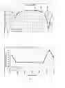
Referring to FIG. 1, a first conventional antenna 1′ comprises a substrate 10′ and an antenna layer 11′ disposed on a top surface of the substrate 10′. The antenna layer 11′ is printed on the substrate 10′ by using conductive ink and comprises a patch 111′ and a feed line 112′. The patch 111′ is a whole without gaps.
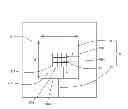
Referring to FIG. 2, a gridded antenna 1 in accordance with a first embodiment of the present disclosure is a revised antenna according to the first conventional antenna 1′. The gridded antenna 1 comprises a substrate 10 and an antenna layer 11 disposed on a top surface of the substrate 10. The antenna layer 11 includes a patch 111 defining a width L, and a feed line 112 extending from the patch 111. The patch 111 includes a number of slots 1110 forming a gridding part 113, and an edge part 114 surrounding the gridding part 113. The feed line 112 is electrically connected to the edge part 114. The gridding part 113 is disposed at a center portion of the patch 111. In this embodiment, the the slots are arranged in a 3 by 3 matrix. The arrangement of the slots, however, is variable according to actual requirements, and the slots may be arranged in matrixes ranging from 3 by 3 to 20 by 20.
The substrate 10 is made from FR-4. The antenna layer 11 is manufactured by printing conductive ink on the substrate 10.
The edge part 114 has a first width a, which is measured from an first side 1131 of the gridding part 113 to a first edge 1111 of the patch 111 opposite to the first side 1131. The edge part 114 has a second width b, which is measured from a second side 1132 of the gridding part 113 to a second edge 1112 of the patch 111 opposite to the second side 1132. A parameter of width_ratio is defined as follows for defining the width of the edge part 114:
Width_ratio=a/L, or Width_ratio=b/W
By simulation, different values of the width_ratio ranging from 0.1 has been studied and it is found that width_ratio has to be at least 0.32 in order to produce almost identical performance characteristics as the first conventional antenna without slots. These can be seen from the simulation results of return Loss and total efficiency shown in FIG. 3 and FIG. 4.
Separate simulations were conducted for the gridded antenna 1 with different number of slots arranged in matrixes from 3 by 3, to 20 by 20. The simulation results suggested that with increasing number of slots in the gridded antenna, its antenna performance characteristics get closer to that of the first conventional antenna. Therefore, the gridded antenna 1 has a reduced conductive area while retaining substantial identical performance characteristics to the conventional antenna. In the embodiment, the patch 111 could be square and rectangular.
A method for manufacturing the gridded antenna comprises steps of: providing a substrate 10;
- forming an antenna layer 11 on the substrate 10 by printing conductive ink, the antenna layer 11 including a patch 111 and a feed line 112, the patch 111 including a plurality of slots 1110 forming a gridding part 113 and an edge part 114 surrounding around the gridding part 113, a ratio of a width of the edge part and that of the gridding part being at least 0.32.
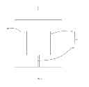
Referring to FIG. 5, an second conventional antenna 2 is a dual-band Planar Inverted-F Antenna (PIFA) working at GSM-850 and PCS-1900 bands, which is made by cutting a thin copper sheet.
Referring to FIG. 6, a gridded antenna 3 in accordance to a second embodiment of the present disclosure is a revised PIFA antenna according to the second conventional antenna 2. The antenna 3 is a metallic sheet. The antenna 3 includes a plurality of slots 30 forming a gridding part 31 and an edge part 32 surrounding around the gridding part 31. The edge part 32 has a width a, and the antenna 3 has a width L. The width a of the edge part 32 satisfies the requirement for width_ratio=a/L=0.32. The total conductive surface area of the second conventional antenna 2 is 696 mm2 and that of the antenna 3 is 485 mm2, hence 30.3% of the conductive area is reduced.
Referring to FIGS. 7 and 8, a comparison of the measured antenna performance characteristics between the second conventional antenna 2 and the revised antenna 3 is shown. It can be observed that the revised antenna 3 is able to generate a return loss and antenna efficiency that matches well to that of the second conventional antenna 2. Hence the gridded antenna 3 has a reduction conductive area while retaining its original performance characteristics.
It will be understood that the above-mentioned particular embodiments is shown and described by way of illustration only. The principles and the features of the present disclosure may be employed in various and numerous embodiments thereof without departing from the scope of the disclosure as claimed. The above-described embodiments illustrate the scope of the disclosure but do not restrict the scope of the disclosure.
Claims
What is claimed is:1. An antenna comprising:
a substrate;
an antenna layer disposed on a top surface of the substrate, including a patch and a feed line electrically connected to the patch, the patch including a plurality of slots disposed at a center portion thereof for forming a gridding part and an edge part surrounding the gridding part; wherein
a ratio of the width of the edge part and the width of the patch is at least 0.32.
2. The antenna as claimed in claim 1, wherein the antenna layer is printed on the substrate with conductive ink.
3. The antenna as claimed in claim 2, wherein the substrate is made of FR-4 substrate.
4. The antenna as claimed in claim 1, wherein the patch is square or rectangular.
5. The antenna as claimed in claim 1, wherein the number of the slots is arranged in matrixes ranging from 3 by 3 to 20 by 20.
6. An antenna comprising:
a metallic sheet including a plurality of slots disposed at a center portion thereof for forming a gridding part and an edge part surrounding the gridding part; wherein
a ratio of the width of the edge part and the width of the patch is at least 0.32.
7. The antenna as claimed in claim 6, wherein the antenna is a PIFA antenna working at GSM-850 and PCS-1900 bands.
8. The antenna as claimed in claim 6, wherein a conductive area of the antenna layer is reduced at least 30% by the slots.
9. A method for manufacturing an antenna, comprising the steps of:
forming an antenna layer, the antenna layer including a plurality of slots forming a gridding part and an edge part surrounding around the gridding part, wherein
a ratio of the width of the edge part and the width of the antenna layer is at least 0.32.
10. The method for manufacturing an antenna as claimed in claim 9, wherein a substrate is provided, and the antenna layer is printed on the substrate with conductive ink.
11. The method for manufacturing an antenna as claimed in claim 10, wherein the antenna layer is made by cutting a copper sheet.
Images & Drawings included:


Sources:
- United States Patent and Trademark Office - verify current appl. status at the USPTO↗
Recent applications in this class:
- » 20250253523 2025-08-07
METAL MESH, THIN FILM SENSOR AND MASK - » 20250239759 2025-07-24
DISPLAY APPARATUS AND HUMAN-COMPUTER INTERACTION APPARATUS - » 20250233302 2025-07-17
ANTENNA DEVICE AND IC CARD PROVIDED THEREWITH - » 20250226575 2025-07-10
LASER DIRECT STRUCTURING ANTENNA ASSEMBLY FOR IN-VIVO DEVICES - » 20250210854 2025-06-26
TERAHERTZ ELEMENT AND SEMICONDUCTOR DEVICE - » 20250118890 2025-04-10
TRANSMISSION DEVICE AND PREPARATION METHOD THEREFOR, AND QUANTUM DEVICE INTEGRATION COMPONENT AND QUANTUM COMPUTER - » 20250105498 2025-03-27
ANTENNA DEVICE AND IC CARD - » 20250079695 2025-03-06
ANTENNA MODULE HAVING PLURALITY OF PRINTED CIRCUIT BOARDS LAMINATED THEREIN, AND ELECTRONIC DEVICE COMPRISING SAME - » 20250055182 2025-02-13
UWB ANTENNA - » 20250046988 2025-02-06
ANTENNA STRUCTURE AND ELECTRONIC DEVICE
Recent applications for this Assignee:
- » 20250106561 2025-03-27
MICROELECTROMECHANICAL SYSTEM MEMBRANE - » 20250042724 2025-02-06
CAPACITIVE SENSING CIRCUIT AND CAPACITIVE SENSING METHOD - » 20240284120 2024-08-22
Acoustic transducer and method for manufacturing acoustic transducer - » 20240284119 2024-08-22
Acoustic transducer and method for manufacturing acoustic transducer - » 20240236551 2024-07-11
LOUDSPEAKER ASSEMBLY AND HAND-HELD DEVICE - » 20240236550 2024-07-11
Sound reproducing apparatus and method - » 20240223942 2024-07-04
Speaker module - » 20240223941 2024-07-04
Speaker module - » 20240223937 2024-07-04
Speaker module - » 20240214749 2024-06-27
MEMS OPTICAL MICROPHONE