DETERMINING A CHARACTERISTIC OF A SIGNAL IN RESPONSE TO A CHARGE ON A CAPACITOR
US20140239933A1
2014-08-28
14/191,078
2014-02-26
Abstract:
In an embodiment, an apparatus includes a charging circuit and a determining circuit. The charging circuit is configured to generate a charge on a capacitor with a first current that is related to a signal having a characteristic, and the determining circuit is configured to determine the characteristic of the signal in response to the charge on the capacitor. For example, such an apparatus can determine an average of an input current to a power supply, or an average of an output current from a power source for the power supply, by mirroring the input current, charging a capacitor with the mirroring current, and determining the voltage across the charged capacitor.
Assignee:
- INTERSIL AMERICAS LLC 235 🇺🇸 Milpitas, CA, United States
Interested in similar patents?
Get notified when new applications in this technology area are published.
Classification:
H02M3/156 » CPC main
Conversion of dc power input into dc power output without intermediate conversion into ac by static converters using discharge tubes with control electrode or semiconductor devices with control electrode using devices of a triode or transistor type requiring continuous application of a control signal using semiconductor devices only with automatic control of output voltage or current, e.g. switching regulators
Description
PRIORITY CLAIM
The present application is a Continuation in Part of copending U.S. patent application Ser. No. 13,829,555, filed 14 Mar. 2013; which application claims priority from copending U.S. Provisional Patent Application No. 61/769,404 filed 26 Feb. 2013; all of the foregoing applications are incorporated herein by reference in their entireties.
SUMMARY
In an embodiment, an apparatus, such as a power-supply controller, includes a charging circuit and a determining circuit. The charging circuit is configured to generate a charge on a capacitor with a first current that is related to a signal having a characteristic, and the determining circuit is configured to determine the characteristic of the signal in response to the charge on the capacitor.
For example, an embodiment of such an apparatus may be able to determine an average of an input current to a power supply, or an average of an output current from a power source for the power supply, by mirroring the input current and charging a capacitor with the mirroring current. To determine the average of the input current, the capacitor effectively integrates the input current over the power-supply switching period, and the current mirror and the capacitor may be designed such that the magnitude of a voltage across the capacitor approximately equals the magnitude of the average input current. To determine the average of the power-source output current, the power-supply controller effectively filters the voltage across the capacitor with an impedance that approximately equals the impedance between the power source and the input node of the power supply.
BRIEF DESCRIPTION OF THE DRAWINGS
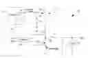
FIG. 1 is a diagram of a power system that includes a power source, a power supply that receives power form the power source, and a load that receives power form the power supply, according to an embodiment.
FIG. 2 is a time plot of the input current to the power supply of FIG. 1, according to an embodiment.
FIG. 3 is a diagram of a power system that includes a power source, a power supply that receives power form the power source, and a load that receives power form the power supply, according to another embodiment.
FIG. 4 is a diagram of the current-mirror circuit of FIG. 3, according to an embodiment.
FIG. 5 is a diagram of the stage of FIG. 3 that generates a representation of the average current output by the power source of FIG. 3, according to an embodiment.
FIG. 6 is a time plot of the voltage across the integrating capacitor of FIG. 3, where the voltage represents the average input current to the power supply of FIG. 3, according to an embodiment.
FIG. 7A is a time plot of the input current to the power supply of FIG. 3, according to an embodiment.
FIG. 7B is a time plot of the average of the input current to the power supply of FIG. 3, and of the average output current from the power source of FIG. 3, according to an embodiment.
FIG. 8A is a time plot of the average output current from a power source to a power supply while the power supply is operating in a current-limiting mode using a conventional technique for determining the average input current to the power supply, according to an embodiment.
FIG. 8B is a time plot of the average output current from a power sourced to a power supply while the power supply is operating in a current-limiting mode using the technique described in conjunction with FIGS. 3-6 for determining the average input current to the power supply, according to an embodiment.
FIG. 9 is a diagram of a system that incorporates the power system or power supply of FIG. 3, according to an embodiment.
DETAILED DESCRIPTION
FIG. 1 is a schematic diagram of a power system 10, which includes a power source 12, a power supply (here a buck converter) 14, and a load 16, according to an embodiment. The power supply 14 converts an input voltage Vin from the power source 12 into a regulated output voltage Vout, which powers the load 16. Where, as in the described embodiment, the power supply 14 is a buck converter, |Vout|<|Vin|; for example, Vin=5 Volts (V) and Vout=1.3 V.
The power source 12 may be modeled as including an ideal DC voltage source 18 and an internal impedance 20. The ideal voltage source 18 is configured to generate a voltage Vsource and to provide an output current Isource, and the impedance 20 has a value of R—although the impedance is described has having only a real impedance value R, it may have a complex value. Therefore, if R>0 and Isource>0, then Vin<Vsource due to the voltage drop across the impedance 20.
The buck-converter power supply 14 includes an input node 22, a power-source bypass capacitor 24, a switching controller 26, high-side and low-side switching transistors 28 and 30, a filter inductor 32, and a filter capacitor 34.
The bypass capacitor 24 prevents voltage oscillations and voltage ringing at the input node 22 by providing a low-impedance path to ground 36 for all non-zero-frequency signals at the input node.
The switching controller 26 controls the timing of the switching of the transistors 28 and 30 in response to Vout, or in response to a feedback signal that is related to Vout, in a manner that maintains Vout at a voltage level that is set by a reference voltage Vref.
The high-side transistor 28, when activated by the controller 26, couples the inductor 32 to the input node 22 such that a current Iin (described below in conjunction with FIG. 2) flows from the input node, through the transistor 28 and the inductor (the low-side transistor 30 is inactive while the high-side transistor is active), and to the filter capacitor 34 and the load 16, thereby energizing the inductor. Iin may not equal Isource due to the presence of the network formed by the source impedance 20 and the bypass capacitor 24.
The low-side transistor 30, when activated by the controller 26, couples the inductor 32 to ground 36 such that a current Ide-energize flows from ground, through the low-side transistor and the inductor (the high-side transistor 28 is inactive while the low-side transistor is active), and to the filter capacitor 34 and the load 16, thereby de-energizing the inductor. As described below in conjunction with FIG. 2, the current Ide-energize typically does not decay all the way to zero before the controller 26 again activates the high-side transistor 28 to repeat the above-described cycle.
The switching of the transistors 28 and 30 generates, at an intermediate node 38 between the transistors, a digital-like voltage that transitions between two levels, approximately Vin and ground.
But the inductor 32 and the capacitor 34 effectively filter the voltage at the intermediate node 38 to generate the regulated DC output voltage Vout.
Furthermore, the load 16 may be any suitable load, such as a microprocessor, a microcontroller, or a memory.
FIG. 2 is a time plot of the input current Iin of FIG. 1, according to an embodiment. The input current Iin has a period of T, which is equal to 1/F, where F is the frequency at which the controller 26 switches the transistors 28 and 30; that is, F is the switching frequency of the power supply 14. Furthermore, the current Iin linearly increases from Ivalley to Ipeak during a portion Ton of the period T; Ton corresponds to the time during which the high-side transistor 28 is active and the low-side transistor 30 is inactive. Moreover, Iin is zero during a portion Toff of the period T; Toff corresponds to the time during which the high-side transistor 28 is inactive and the low-side transistor 30 is active. In addition, Ide-energize is zero during Ton, and decays linearly from Ipeak to Ivalley during Toff; that is, while Iin is non-zero, Ide-energize is zero, and while Iin is zero, Ide-energize is non-zero. And the duty cycle D of the power supply 14 equals Ton/T.
Referring to FIGS. 1 and 2, the operation of the power system 10 of FIG. 1 is described, according to an embodiment.
At a time t0, the controller 26 activates the high-side transistor 28 and deactivates the low-side transistor 30 (the controller may deactivate the low-side transistor first to prevent a crow-bar current from simultaneously flowing through both transistors) such that the current Iin flows from the node 22, through the high-side transistor and inductor 32, and to the capacitor 34 and load 16. Because the current through an inductor cannot change instantaneously, the value of Iin at t0 equals Ivalley, which is the value of the de-energizing current Ide-energize (not shown in FIG. 2) that was flowing through the inductor 32 immediately prior to t0.
During Ton between the time t0 and a time t1, the current Iin increases linearly. The voltage V across an inductor and the current I through an inductor are related according to the following equations:
V=L(dI/dt) (1)
such that
dI/dt=V/L (2)
For the power-supply system 10, one can assume that during Ton, the voltage across the high-side transistor 28 is negligible such that the voltage V across the inductor 32 equals (Vin−Vout)/L, and such that:
dIin/dt=(Vin−Vout)/L (3)
And because one can assume that during Ton, Vin and Vout are constant, dIin/dt, which is the rate at which Iin is increasing during Ton, is also a constant, such that Iin increases according to a straight line 40 having a constant slope that is equal to (Vin−Vout)/L.
At the time t1, the controller 26 activates the low-side transistor 30 and deactivates the high-side transistor 28 (the controller may deactivate the high-side transistor first to prevent a crow-bar current from simultaneously flowing through both transistors) such that the current Ide-energize flows from ground 36, through the low-side transistor and inductor 32, and to the capacitor 34 and load 16. Because the current through an inductor cannot change instantaneously, the value of Ide-energize at t1 equals Ipeak, which is the value of the input current Iin that was flowing through the inductor 32 immediately prior to t1.
Further at the time t1, the current Iin falls rapidly to zero, and remains at zero until a time t2, at which time the above-described cycle repeats. Also, between the times t1 and t2, Ide-energize (not shown in FIG. 2) decays linearly with a slope of (Vout)/L (the voltage across the low-side transistor 30 can be assumed to be negligible such that the inductor 32 can be assumed to be coupled between Vout and ground).
Still referring to FIGS. 1 and 2, alternate embodiments of the power system 50 are contemplated. For example, the power supply 14 may include one or more additional components not described above, or may omit one or more of the above-described components.
Furthermore, in some applications, one may wish to know the average of Iin, i.e., Iin—avg, for each switching period T, the average of Isource, i.e., Isource—avg for each switching period T, or both Iin—avg and Isource—avg for each switching period T. For example, one may wish to limit Iin—avg to prevent damage to the power supply 14. Or, one may wish to limit Isource—avg to prevent damage to the power source 12; for example, if the power source is a battery, then one may wish to limit Isource—avg to prevent overheating or premature discharge of the power source.
One way to determine Iin—avg over a switching period T is to insert a sense resistor between the node 22 and the high-side transistor 28, and to low-pass filter this sense voltage to generate a resulting low-pass-filtered voltage that is proportional to Iin—avg.
But there may be some problems with this approach. For example, the sense resistor may significantly decrease the efficiency of the power supply 14, and the resulting low-pass-filtered voltage may be significantly delayed relative to Iin and Iin—avg; this delay may render a control loop or other circuitry for limiting Iin—avg too slow, as described below in conjunction with FIG. 6A.
Another way to determine Iin—avg over a switching period T is to use a processor to calculate Iin—avg according to the following equation:
I in_avg = 1 T ∫ 0 T I in t ( 4 )
For example, for Iin of FIG. 2, per equation (4), Iin—avg over a switching period T is given by the following equation:
Iin—avg=Ton/T(Ivalley+Ipeak/2) (5)
But a problem with this approach is that it may require complex circuitry to measure, for example, Ivalley, Ipeak, and Ton, and to calculate Iin—avg according to equation (4) or equation (5).
FIG. 3 is a diagram of a power system 50, which, in addition to the power source 12, power supply 14, and load 16, includes a determiner circuit 52 configured to determine Iin—avg and Isource—avg, according to an embodiment, and like numbers are used to label components common to the power systems 10 (FIGS. 1) and 50; therefore, common components already described above in conjunction with FIGS. 1 and 2 are not described in conjunction with FIG. 3.
The determiner circuit 52 includes a current mirror 54, an integrating capacitor 56, a sample-and-hold circuit 58, a reset circuit 60, and a stage 62 effectively configured to determine Isource—avg in response to Iin—avg.
The current mirror 54 receives the gate and source voltages Vg and Vs from the NMOS high-side transistor 28, and is configured to generate a current Iin—integrate in response to Vg and Vs. Iin—integrate is i related to Iin by a scale factor S according to the following equation:
Iin—integrate≈S·Iin (6)
where S<<1 such that the current Imirror that the current mirror 54 draws from Vin can be considered negligible, and, therefore, such that one can assume that Iin flows from the node 22 and entirely through the high-side transistor 28 when the high-side transistor is active. For example, S may be in a range of approximately 1×10⁻³−1×10⁻⁶.
The integrating capacitor 56 receives, and effectively integrates, the current Iin—integrate from the current mirror 54; that is, as described below, the magnitude of the charge stored on the integrating capacitor, and the magnitude of the voltage across this capacitor, are proportional to, and may be equal to, the magnitude of Iin—avg. For example, as described below in conjunction with FIG. 6, one can determine Iin—avg from the voltage across the integrating capacitor 56 at the end of each switching cycle of the power system 50.
The sample-and-hold circuit 58 samples and holds the voltage across the integrating capacitor 56 at the end of each switching cycle, and, after the sample-and-hold circuit samples and holds this capacitor voltage, the reset circuit 60 discharges the integrating capacitor to ready the integrating capacitor for the next switching cycle. The sample-and-hold circuit 58 includes a sample switch 70 (e.g., a transistor), a buffer 72, a hold capacitor 74, and another buffer 76, which generates a voltage VIin—avg, which represents Iin—avg. And the reset circuit 60 includes an NMOS transistor.
The stage 62 is configured to generate Isource—avg from the power source 12 in response to the voltage VIin—avg. For example, as described below in conjunction with FIGS. 3 and 5-7B, the stage 62 does this by effectively filtering VIin—avg with approximately the same effective impedance as the impedance of the network between the node 22 and the ideal voltage source 18.
Before describing the operation of the power system 50, the theory behind the determiner circuit 52 is described.
The current I through, and the voltage V across, a capacitor C, are related according to the following equation:
I=C(dV/dt) (7)
And from equation (7), one can derive the following equation:
V = 1 C ∫ I t ( 8 )
Therefore, referring to FIGS. 2 and 3 and equations (6)-(8), VIin—avg across the integrating capacitor 56 and the current Iin are related by the following equation:
V Iin_avg = 1 C ∫ 0 T I in_integrate t = 1 C ∫ 0 T ( I in · S ) t = S C ∫ 0 T I in t ( 9 )
And equation (9) yields the following equation:
V Iin_avg · C S = ∫ 0 T I in t ( 10 )
Furthermore, equation (4) yields the following equation:
T·Iin—avg=∫0TIindt (11)
Therefore, combining equations (10) and (11) yields the following equation:
V Iin_avg · C S = T · I in_avg ( 12 )
Ignoring the units of the terms in equation (12), setting the magnitude of VIin—avg equal to the magnitude of Iin—avg yields the following equations for the value C of the integrating capacitor 56 in Farads:
C=|T·S| (13)
C=|(S)/F| (14)
Therefore, if one selects the value C of the integrating capacitor 56 per equation (13) or (14), then the magnitude of the voltage VIin—avg that appears across the integrating capacitor, and that is output by the sample-and-hold circuit 58, at the end of a switching period equals the magnitude of the average input current Iin—avg over the same switching period.
FIG. 4 is a diagram of the current mirror 54 of FIG. 3, according to an embodiment.
The current mirror 54 includes an NMOS sense transistor 64, a PMOS load transistor 66, and a high-gain amplifier 68. The NMOS sense transistor 64 has a channel width/length ratio that equals a scale factor S times the channel width/length ratio of the NMOS high-side transistor 28 of FIG. 3. In this example, as described above, S<<1 (for example, in a range of approximately 1×10⁻³−1×10⁻⁶), although in another example S may be less than but closer to one, or greater than or equal to one.
Still referring to FIG. 4, the current mirror 54 operates as follows to generate Iin—integrate per equation (6) above.
The amplifier 68 and the PMOS load transistor 66 together operate to maintain the voltage at the source of the NMOS sense transistor 64 at approximately the same voltage Vs as the source of the NMOS high-side transistor 28 of FIG. 3. In detail, the amplifier 68 controls the voltage at the gate of the transistor 66 so as to cause the voltage (i.e., the source voltage of the sense transistor 64) at its inverting input node to be approximately equal to the voltage (i.e., the source voltage Vs of the high-side transistor 28) at its non-inverting node. Furthermore, the current mirror 54 may include additional circuitry, such as feedback compensation circuitry, within, or coupled to, the amplifier 68.
Because the gate voltages of the transistors 28 and 64 are approximately equal to one another, and because the source voltages of these same transistors are also approximately equal to one another, the gate-to-source voltages of these transistors are approximately equal to one another; therefore, the sense transistor 64 draws the current Iin—integrate, which is given by the following equation, which is the same as equation (6) above:
Iin—scale≈S·Iin (15)
Still referring to FIG. 4, alternate embodiments of the current mirror 54 are contemplated. For example, the current mirror 54 may include any suitable current-mirror circuit topology.
FIG. 5 is a diagram of the stage 62 of FIG. 3, according to an embodiment. As described above, the stage 62 presents to the voltage Vin—avg an impedance that is equivalent to the impedance presented to the current Iin by the transistor 28, capacitor 24, and power-source resistance 20 of FIG. 3.
The stage 62 includes resistors 82 and 84, and a capacitor 86. In operation, the voltage Vin—avg causes a current I1 to flow through the resistor 82, and a current I2 to flow through the resistor 84. The current I2 charges the capactor 84 to the voltage Vsource—avg, which is proportional to the average Isource—avg of the current Isource from the power source 12 of FIG. 3. In a manner similar to that described above in conjunction with the generating of Vin—avg, one can select the values of the resistors 82 and 84 and the capacitor 86 such that ignoring units, |Vsource—avg|=|Isource—avg|.
FIG. 6 is a time plot of the voltage VIin—avg across the integrating capacitor 56 of FIG. 3, and at the output of the sample-and-hold circuit 58 of FIG. 3, according to an embodiment.
Referring to FIGS. 3 and 6, the operation of the power system 50 is described, according to an embodiment. Because the operation of the power supply 14 is the same as described above in conjunction with FIGS. 1 and 2, only the operation of the determiner 52 is described in detail.
At the time t0, the controller 26 activates the high-side transistor 28 such that the input current Iin begins to flow through the high-side transistor as described above in conjunction with FIGS. 1 and 2—as described above, in this example Imirror is small enough so that one can assume that Iin flows from the node 22 through the high-side transistor.
In response to the current Iin beginning to flow through the high-side transistor 28, the current mirror 54 begins to generate Iin—integrate.
And Iin—integrate begins to charge, and, therefore, to develop a voltage across, the integrating capacitor 56.
During the portion Ton of the switching cycle between the times t0 and t1, Iin increases linearly as shown in FIG. 2.
Therefore, because Iin—integrate mirrors Iin, Iin—integrate also increases linearly between the times t0 and t1.
Per equation (8), because Iin—integrate increases linearly, Vin—avg across the capacitor 56 increases parabolically; i.e., the wave form of Vin—avg is a parabola.
At the time t1, the controller 26 deactivates the high-side transistor 28 such that Iin rapidly decreases to zero as described above in conjunction with FIGS. 1 and 2.
Also at the time t1, the controller 26 deactivates the current mirror 54 such that Iin—integrate also rapidly decreases to zero.
Consequently, at the time t1, the voltage VIin—avg across the integrating capacitor 56 stops increasing, and remains at an approximately constant level Vfinal due to the high impedances that the inactive current mirror 54, open switch 70, and inactive reset circuit 60 present to the integrating capacitor.
At some point between the time t1 and a time t3, the controller 26 closes the switch 70 so as to charge, via the buffer 72, the hold capacitor 74 approximately to the voltage level Vfinal that exists across the integrating capacitor 56.
And, after the hold capacitor 74 is charged to approximately Vfinal, the controller 26 opens the switch 70.
Then, at the time t3, the controller 26 activates the transistor of the refresh circuit 60 to discharge the integrating capacitor 56 in anticipation of the next switching cycle of the power system 50.
FIG. 7A is a time plot of the input current Iin from the input node 22 of FIG. 3 in response to a step change in the load current ILoad through the load 16 of FIG. 3, according to an embodiment.
FIG. 7B is a time plot of Vin—avg, which represents the average input current Iin—avg, and of Vsource—avg, which represents the average source current Isource—avg from the power source 12 of FIG. 3, in response to a step change in the load current ILoad, according to an embodiment. Both Vin—avg and Vsource—avg are shown on a cycle-by-cycle basis.
Referring to FIGS. 3, 7A, and 7B, the operation of the stage 62 of the determiner circuit 52 is described, according to an embodiment.
As described above, the stage 62 generates a voltage Vsource—avg having a magnitude and phase that are approximately proportional to, or that are approximately equal to, the magnitude and phase of Isource—avg.
Before the time t0, assume that the bypass capacitor 24 is charged to Vin, and that because Iin=0, Vin=Vsource.
Before or at the time t0, a step increase in the load current ILoad occurs, and the network formed, at least in part, by the inductor 32 and the capacitor 34, causes the current through the inductor to “ring” during a transient-response period Ttransient.
At the time t0, the controller 26 activates the high-side transistor 28, which effectively couples this ringing to the node 22, and, therefore, causes Iin to ring as shown in FIG. 7A.
Because an impedance network formed primarily by the internal impedance 20 of the power source 12, the bypass capacitor 24, and the active transistor 28 is effectively “seen” by the ideal voltage source 18, Isource equals Iin as modified, or filtered, by this impedance network; that is, one can consider Iin an input to this network, and Isource as an output of this network.
As described above, in an embodiment, the magnitude of VIin—avg approximately equals the magnitude of Iin—avg on a cycle-by-cycle basis.
Therefore, if one inputs VIin—avg to a filter having the same effective transfer function as that of the network formed by the internal resistance 20, the bypass capacitor 24, and the active transistor 28, then the output Vsource—avg of this filter has a magnitude and a phase that are approximately equal to the magnitude and the phase of Isource—avg.
Consequently, the stage 62 may include a filter that, effectively, is the same as the network formed by the resistance 20, the bypass capacitor 24, and the active transistor 28, or that may be topologically different (or that may be implemented digitally) but that has the same effective transfer function as this network, such that the magnitude of Vsource—avg is approximately proportional or approximately equal to the magnitude of Isource—avg, and the phase of Vsource—avg is approximately equal to the phase of Isource—avg. The terms “effectively” and “effective” here indicate that the stage 62 also accounts for Iin and lin—avg being currents and Vin—avg being a voltage; that is, the impedance of the stage 62, which filters the voltage Vin—avg, is equivalent to, but may not be identical to, the impedance formed by the source resistance 20, capacitor 24, and active transistor 28, which impedance filters the current I,n.
Referring to FIGS. 3 and 6-7B, alternate embodiments of the power system 50 are contemplated. For example, the power supply 15 may be any type of switching power supply other than a buck converter. Furthermore, the determiner 52 may be controlled by other than the switching controller 26, and may be disposed in a circuit other than a power supply. Moreover, the integrating current Iin—integrate may be generated by any suitable circuit other than the current mirror 54 of FIGS. 3 and 4. In addition, the calculation of VIin—avg may be implemented in software or in firmware, such as by an instruction-executing processor, or in a combination or subcombination of software, firmware, and hardware. Furthermore, the stage 62 may be implemented in software or firmware, such as by an instruction-executing processor, or in a combination or subcombination of software, firmware, and hardware. Moreover, the above-described current-average determining technique may be used to determine the average of signals other than a power-supply input current. For example, the technique may be used in a battery charger to determine the average charging current being supplied to a battery; the charger may include a circuit for limiting the average charging current in response to this determination so as to prevent damage to the battery. In addition, the technique, or an embodiment thereof, may be used to determine a characteristic other than an average of a signal other than a current. Furthermore, one or more components of the power supply 14 and determiner 52 may be disposed on a power-supply controller, which may be an integrated circuit. In addition, one or more components of the power supply 14 and determiner 52 may be disposed in a power-supply module.
FIG. 8A is a time plot of the average source current Isource—avg from the power source 12 of the power system 10 of FIG. 1 in response to a step increase in Iin—avg, where the power system is configured to limit Isource—avg to a maximum threshold ILimit, according to an embodiment.
FIG. 8B is a time plot of the average source current Isource—avg from the power source 12 of the power system 50 of FIG. 3 in response to a step increase in Iin—avg, where the power system is configured to limit Isource—avg to ILimit, according to an embodiment.
In the below-described example, ILimit=2 A.
The ability of the power system 10 (FIG. 1) to limit Isource—avg to ILimit is now compared to the ability of the power system 50 (FIG. 3) to limit Isource—avg to ILimit in conjunction with FIGS. 1, 3, and 7B-8B. For example, the power systems 10 and 50 may limit Isource—avg to prevent damage to the power source 12 (e.g., a battery). Because such current limiting, and the circuitry for performing such current limiting, is conventional, a detailed description of such current limiting and current-limiting circuitry is omitted for brevity.
Because, in a steady state, Isource—avg=Iin—avg, a power system such as the power system 10 or 50, may limit Isource—avg by monitoring and limiting Iin—avg.
As described above in conjunction with FIGS. 1 and 2, to determine Iin—avg, the power system 10 may include a sense resistor in series with Iin, and a low-pass filter that filters the voltage across the sense resistor to generate a filtered voltage that is related to Iin—avg.
But as also described above, such a low-pass filter may cause a delay between Iin and the filtered voltage; that is, the filtered voltage may lag the actual average Iin—avg of Iin.
Referring to FIG. 8A, if this filtered voltage is used to monitor Iin—avg, and to limit Iin—avg, and, therefore, to limit Isource—avg, to a limit threshold ILimit in response to the monitored Iin—avg, then by the time that the filtered voltage indicates that Iin—avg has exceeded ILimit and the limit circuitry can limit Iin—avg to Isource—avg may have already exceeded the limit. In this example, Isource—avg exceeds ILimit=2 A from a time t0, when the step increase in Iin—avg begins, to a time t1, when the limit circuitry of the power system 10 finally is able to limit Isource—avg to ILimit. That is, the time between t0 and t1 is the lag time between the start of the step increase in Iin—avg and the limiting of Isource—avg to ILimit by the power system 10.
Unfortunately, this lag time between t0 and t1 may be long enough to allow the power source 12 to be damaged by an average source current Isource—avg that is too high for too long.
In contrast, referring to FIG. 7B, because the determiner 52 of the power system 50 (FIG. 3) has no such lag time, VIin—avg, which represents Iin—avg, leads Vsource—avg, which represents Isource—avg, just as Iin—avg leads Isource—avg.
Consequently, referring to FIG. 8B, when the power system 50 (FIG. 3) monitors VIin—avg and limits VIin—avg to ILimit in response to VIin—avg equaling or exceeding ILimit, the power system 50 is able to limit Isource—avg to ILimit before Isource—avg exceeds ILimit.
Referring again to FIGS. 3-7B, uses for Vin—avg other than limiting Iin, Iin—avg, Isource—avg are contemplated, and uses for Vsource—avg are also contemplated.
For example, if the power source 12 is, or includes, a battery, then the power system 50 can be configured to monitor Isource—avg by monitoring Vsource—avg so as to estimate the charge remaining on the battery, or the remaining time before the battery would need to be replaced or recharged. This technique may be particularly useful where the battery has a known discharge profile.
In another example, the power system 50 can be configured to monitor Isource—avg by monitoring Vsource—avg, and to limit or reduce Isource—avg in response to Vsource—avg equaling or exceeding a threshold. This may be different than limiting Isource—avg per FIG. 8B, because the reducing may be done more slowly, or in response to a low-pass-filtered version of Vsource—avg exceeding the threshold (i.e., Vsource—avg exceeding the threshold over an extended period of time).
In yet another example, the power system 50 can be configured to monitor Vin in a conventional manner, to monitor Isource—avg by monitoring Vsource—avg, and, in response to the monitored Vin and Vsource—avg, to control Isource—avg so as to maintain the power source 12 within a safe voltage-current operating region.
And in still another example, the power system 50 can be configured to monitor Isource—avg by monitoring Vsource—avg, and, in response to the monitored Vsource—avg, to control a charging circuit to attain a highest safe, or otherwise allowed, level of Isource—avg, or of a charging current, as quickly as possible without overshooting a maximum limit of Isource—avg or of the charging current. Such a technique may allow charging or recharging of a battery or other device more quickly than other chargers without causing damage to the charging circuit or to the battery or other device.
Furthermore, in at least some of the above-described examples, the power system 50 may be able to achieve a similar result by monitoring Vin—avg instead of, or in addition to, monitoring Vsource—avg.
FIG. 9 is a block diagram of an embodiment of a computer system 100, which incorporates the power system 50 (or only the power supply 14) of FIG. 3, according to an embodiment. Although the system 100 is described as a computer system, it may be any system for which an embodiment of the power system 50 (or only the power supply 14) is suited.
The system 100 includes computing circuitry 102, which, in addition to the supply system 50 (or only the supply 14) of FIG. 3, includes a processor 104 powered by the system (or only the supply), at least one input device 106, at least one output device 108, and at least one data-storage device 110.
In addition to processing data, the processor 104 may program or otherwise control the system 50 (or only the supply 14). For example, the functions of the power-supply controller 26 may be performed by the processor 104.
The input device (e.g., keyboard, mouse) 106 allows the providing of data, programming, and commands to the computing circuitry 102.
The output device (e.g., display, printer, speaker) 108 allows the computing circuitry 102 to provide data in a form perceivable by a human operator.
And the data-storage device (e.g., flash drive, hard disk drive, RAM, optical drive) 110 allows for the storage of, e.g., programs and data.
From the foregoing it will be appreciated that, although specific embodiments have been described herein for purposes of illustration, various modifications may be made without deviating from the spirit and scope of the disclosure. Furthermore, where an alternative is disclosed for a particular embodiment, this alternative may also apply to other embodiments even if not specifically stated. Moreover, the components described above may be disposed on a single or multiple IC dies to form one or more ICs, these one or more ICs may be coupled to one or more other ICs. In addition, any described component or operation may be implemented/performed in hardware, software, firmware, or a combination of any two or more of hardware, software, and firmware. Furthermore, one or more components of a described apparatus or system may have been omitted from the description for clarity or another reason. Moreover, one or more components of a described apparatus or system that have been included in the description may be omitted from the apparatus or system.
Claims
What is claimed is:1. An apparatus, comprising:
a charging circuit configured to generate a charge on a capacitor with a first current that is related to a signal having a characteristic; and
a determining circuit configured to determine the characteristic of the signal in response to the charge on the capacitor.
2. The apparatus of claim 1, further comprising the capacitor.
3. The apparatus of claim 1 wherein the signal includes a power-supply input current.
4. The apparatus of claim 1 wherein the signal includes a current generated by a power source that provides power to a power supply.
5. The apparatus of claim 1, further comprising:
wherein the signal includes a second current; and
a mirror circuit configured to generate the first current in response to the second current.
6. The apparatus of claim 1 wherein the determining circuit is configured to determine the characteristic of the signal in response to a voltage across the capacitor.
7. The apparatus of claim 1, further comprising:
a filter configured to generate a filtered voltage in response to a voltage across the capacitor; and
wherein the determining circuit is configured to determine the characteristic of the signal in response to the filtered voltage.
8. The apparatus of claim 1, further comprising:
a filter configured to generate a filtered voltage in response to a voltage across the capacitor; and
wherein the determining circuit is configured to determine a characteristic of another signal in response to the filtered voltage.
9. The apparatus of claim 1 wherein the determining circuit is configured to determine that a magnitude of the characteristic of the signal is approximately equal to a magnitude of a voltage across the capacitor.
10. The apparatus of claim 1 wherein the characteristic includes an average.
11. A power supply, comprising:
a capacitor;
a charging circuit configured to generate a charge on the capacitor with a first current that is related to a signal that has a characteristic; and
a determining circuit configured to determine the characteristic of the signal in response to the charge on the capacitor.
12. The power supply of claim 11, further comprising:
wherein the signal includes a second current; and
an inductor configured to conduct the second current.
13. The power supply of claim 11, further comprising:
wherein the signal includes a second current; and
an input node configured to receive the second current.
14. The power supply of claim 11, further comprising:
wherein the signal includes a second current; and
an input node configured to receive a current that is related to the second current.
15. The power supply of claim 11, further comprising:
wherein the signal includes an input current;
an input node configured to receive a source current from a power source and to provide the input current;
a filter configured to generate a filtered voltage in response to a voltage across the capacitor; and
wherein the determining circuit is configured to determine a characteristic of the source current in response to the filtered voltage.
16. The power supply of claim 11, further comprising:
wherein the signal includes an input current;
an input node configured to receive a source current from a power source and to provide the input current;
a filter configured to generate a filtered voltage in response to a voltage across the capacitor; and
wherein the determining circuit is configured to determine an average of the source current in response to the filtered voltage.
17. A system, comprising:
a power supply, including
a capacitor,
a charging circuit configured to generate a charge on the capacitor with a first current that is related to a signal that has a characteristic, and
a determining circuit configured to determine the characteristic of the signal in response to the charge on the capacitor; and
a load coupled to the power supply.
18. The system of claim 17, further comprising:
wherein the power supply includes an input node;
wherein the signal includes a second current; and
a power source configured to provide the second current to the input node.
19. The system of claim 17, further comprising:
wherein the power supply includes an input node;
wherein the signal includes a second current; and
a power source configured to provide a third current to the input node, the third current being related to the second current.
20. The system of claim 17, further comprising:
wherein the power supply includes an input node;
wherein the signal includes an input current from the input node;
a power source configured to provide a source current to the input node;
a filter configured to generate a filtered voltage in response to a voltage across the capacitor; and
wherein the determining circuit is configured to determine an average of the source current in response to the filtered voltage.
21. The system of claim 17, further comprising:
wherein the power supply includes an input node;
wherein the signal includes an input current from the input node;
a battery configured to provide a source current to the input node;
a filter configured to generate a filtered voltage in response to a voltage across the capacitor; and
wherein the determining circuit is configured to determine an average of the source current in response to the filtered voltage.
22. The system of claim 17 wherein the power supply includes a buck converter.
23. A method, comprising:
generating a charge on a capacitor with a first current that is related to a signal having a characteristic; and
determining the characteristic of the signal in response to the charge on the capacitor.
24. The method of claim 23, further comprising:
wherein the signal includes a second current; and
providing the second current to a power supply.
25. The method of claim 23, further comprising:
wherein the signal includes a second current; and
generating the second current with a power source.
26. The method of claim 23, further comprising:
wherein the signal includes a power-supply input current;
generating the power-supply input current in response to a source current from a power source;
generating a filtered voltage in response to a voltage across the capacitor; and
determining an average of the source current in response to the filtered voltage.
27. The method of claim 23, further comprising determining the characteristic of the signal in response to a voltage across the capacitor.
28. A power-supply controller, comprising:
a charging circuit configured to generate a charge on a capacitor with a first current that is related to a signal having a characteristic; and
a determining circuit configured to determine the characteristic of the signal in response to the charge on the capacitor.
Images & Drawings included:


Sources:
- United States Patent and Trademark Office - verify current appl. status at the USPTO↗
Similar patent applications:
Recent applications in this class:
- » 20250175078 2025-05-29
Dual-Input Bus Architecture - » 20250149980 2025-05-08
Power Supply Including a Reconfigurable Power Converter - » 20250141355 2025-05-01
SEMICONDUCTOR DEVICE AND METHOD FOR OPERATING SEMICONDUCTOR DEVICE - » 20250132670 2025-04-24
CURRENT BALANCING CIRCUITS AND TECHNIQUES - » 20250096678 2025-03-20
SWITCHING CYCLE ADAPTIVE CONTROL METHOD FOR SWITCHING POWER SUPPLY - » 20250096677 2025-03-20
MULTI-VOLTAGE DRIVING CONTROL METHOD, APPARATUS, AND DEVICE, AND COMPUTER-READABLE STORAGE MEDIUM - » 20250079983 2025-03-06
AIRCRAFT POWER CONTROL DEVICE, AIRCRAFT COMPRISING AN AIRCRAFT POWER CONTROL DEVICE, AND METHOD OF CONTROLLING AN AIRCRAFT POWER CONTROL DEVICE - » 20250070664 2025-02-27
TRIMMING CIRCUIT FOR BANDGAP REFERENCES - » 20250038662 2025-01-30
SEMICONDUCTOR CIRCUIT DEVICE AND SWITCHING REGULATOR - » 20250038661 2025-01-30
SEMICONDUCTOR CIRCUIT DEVICE AND SWITCHING REGULATOR
Recent applications for this Assignee:
- » 20200266159 2020-08-20
Method of making a stacked inductor-electronic package - » 20200259352 2020-08-13
Regulator with high speed nonlinear compensation - » 20200136397 2020-04-30
Voltage converters and methods for use therewith - » 20190294225 2019-09-26
Apparatuses and methods for encapsulated devices - » 20190280597 2019-09-12
SWITCHING POWER SUPPLY FOR LOW STEP DOWN CONVERSION RATIO WITH REDUCED SWITCHING LOSSES - » 20190173383 2019-06-06
Buck-boost converter power supply with drive circuit - » 20190138070 2019-05-09
System and methods for substrates - » 20190058400 2019-02-21
Method and system controlling DC-DC voltage converters using tracking signal - » 20190056454 2019-02-21
Systems and methods for an open wire scan - » 20190004577 2019-01-03
Method and system for reducing transients in DC-DC converters