Organic electroluminescent materials and devices
US20140264292A1
2014-09-18
13/803,044
2013-03-14
✅ Patent granted
US 9,419,225 B2
2016-08-16
-
-
Ruiyun Zhang
Duane Morris LLP
2034-02-19
Abstract:
A compound according to a formula I, devices incorporating the same, and formulations including the same are described. The compound according to the formula I can have the structure
wherein R1, R2, R3, R4, R5 and R6 each represent mono, di, tri, tetra substitutions, or no substitution, R9 represents mono, di, tri substitutions, or no substitution, R1, R2, R3, R4, R5, R6 and R9 are each independently selected from the group consisting of hydrogen, deuterium, halide, alkyl, cycloalkyl, heteroalkyl, arylalkyl, alkoxy, aryloxy, amino, silyl, alkenyl, cycloalkenyl, heteroalkenyl, alkynyl, aryl, heteroaryl, acyl, carbonyl, carboxylic acid, ester, nitrile, isonitrile, sulfanyl, sulfinyl, sulfonyl, phosphino, and combinations thereof. A1, A2, A3, A4, A5, and A6 are each independently selected from N or C and n is an integer from 1 to 20.
Inventors:
- Chuanjun Xia 357 🇺🇸 Lawrenceville, NJ, United States
- Vadim Adamovich 96 🇺🇸 Yardley, PA, United States
- Lichang Zeng 102 🇺🇸 Lawrenceville, NJ, United States
- Yonggang Wu 2 🇨🇳 Changsha, China
Assignee:
- UNIVERSAL DISPLAY CORPORATION 1,770 🇺🇸 Ewing, NJ, United States
Applicant:
Interested in similar patents?
Get notified when new applications in this technology area are published.
Classification:
H01L51/0054 » CPC main
Solid state devices using organic materials as the active part, or using a combination of organic materials with other materials as the active part; Processes or apparatus specially adapted for the manufacture or treatment of such devices, or of parts thereof; Selection of organic semiconducting materials, e.g. organic light sensitive or organic light emitting materials; Macromolecular systems with low molecular weight, e.g. cyanine dyes, coumarine dyes, tetrathiafulvalene; Polycyclic condensed aromatic hydrocarbons, e.g. anthracene containing four rings, e.g. pyrene
H01L51/0067 » CPC further
Solid state devices using organic materials as the active part, or using a combination of organic materials with other materials as the active part; Processes or apparatus specially adapted for the manufacture or treatment of such devices, or of parts thereof; Selection of organic semiconducting materials, e.g. organic light sensitive or organic light emitting materials; Macromolecular systems with low molecular weight, e.g. cyanine dyes, coumarine dyes, tetrathiafulvalene aromatic compounds comprising a hetero atom, e.g.: N,P,S comprising only nitrogen as heteroatom
H01L51/0072 » CPC further
Solid state devices using organic materials as the active part, or using a combination of organic materials with other materials as the active part; Processes or apparatus specially adapted for the manufacture or treatment of such devices, or of parts thereof; Selection of organic semiconducting materials, e.g. organic light sensitive or organic light emitting materials; Macromolecular systems with low molecular weight, e.g. cyanine dyes, coumarine dyes, tetrathiafulvalene aromatic compounds comprising a hetero atom, e.g.: N,P,S; Polycyclic condensed heteroaromatic hydrocarbons comprising only nitrogen in the heteroaromatic polycondensed ringsystem, e.g. phenanthroline, carbazole
C07D209/86 » CPC further
Heterocyclic compounds containing five-membered rings, condensed with other rings, with one nitrogen atom as the only ring hetero atom; Ring systems containing three or more rings [b, c]- or [b, d]-condensed; Carbazoles; Hydrogenated carbazoles with only hydrogen atoms, hydrocarbon or substituted hydrocarbon radicals, directly attached to carbon atoms of the ring system
C09B57/10 » CPC further
Other synthetic dyes of known constitution Metal complexes of organic compounds not being dyes in uncomplexed form
C07D403/04 » CPC further
Heterocyclic compounds containing two or more hetero rings, having nitrogen atoms as the only ring hetero atoms, not provided for by group containing two hetero rings directly linked by a ring-member-to-ring-member bond
C09K2211/1007 » CPC further
Chemical nature of organic luminescent or tenebrescent compounds; Non-macromolecular compounds; Carbocyclic compounds Non-condensed systems
C09B57/008 » CPC further
Other synthetic dyes of known constitution Triarylamine dyes containing no other chromophores
C09B57/00 » CPC further
Other synthetic dyes of known constitution
C09K11/06 » CPC further
Luminescent, e.g. electroluminescent, chemiluminescent materials containing organic luminescent materials
C09K2211/1029 » CPC further
Chemical nature of organic luminescent or tenebrescent compounds; Non-macromolecular compounds; Heterocyclic compounds characterised by ligands containing one nitrogen atom as the heteroatom
C07D401/04 » CPC further
Heterocyclic compounds containing two or more hetero rings, having nitrogen atoms as the only ring hetero atoms, at least one ring being a six-membered ring with only one nitrogen atom containing two hetero rings directly linked by a ring-member-to-ring-member bond
H01L51/0081 » CPC further
Solid state devices using organic materials as the active part, or using a combination of organic materials with other materials as the active part; Processes or apparatus specially adapted for the manufacture or treatment of such devices, or of parts thereof; Selection of organic semiconducting materials, e.g. organic light sensitive or organic light emitting materials; Coordination compounds, e.g. porphyrin; Metal complexes comprising a IIIB-metal (B, Al, Ga, In or TI), e.g. Tris (8-hydroxyquinoline) gallium (Gaq3) comprising aluminium, e.g. Alq3
H01L51/0085 » CPC further
Solid state devices using organic materials as the active part, or using a combination of organic materials with other materials as the active part; Processes or apparatus specially adapted for the manufacture or treatment of such devices, or of parts thereof; Selection of organic semiconducting materials, e.g. organic light sensitive or organic light emitting materials; Coordination compounds, e.g. porphyrin; Transition metal complexes, e.g. Ru(II)polypyridine complexes comprising Iridium
H01L51/5016 » CPC further
Solid state devices using organic materials as the active part, or using a combination of organic materials with other materials as the active part; Processes or apparatus specially adapted for the manufacture or treatment of such devices, or of parts thereof specially adapted for light emission, e.g. organic light emitting diodes [OLED] or polymer light emitting devices [PLED]; Electroluminescent [EL] layer Triplet emission
H01L51/00 IPC
Solid state devices using organic materials as the active part, or using a combination of organic materials with other materials as the active part; Processes or apparatus specially adapted for the manufacture or treatment of such devices, or of parts thereof
H01L51/50 IPC
Solid state devices using organic materials as the active part, or using a combination of organic materials with other materials as the active part; Processes or apparatus specially adapted for the manufacture or treatment of such devices, or of parts thereof specially adapted for light emission, e.g. organic light emitting diodes [OLED] or polymer light emitting devices [PLED]
C09K2211/1044 » CPC further
Chemical nature of organic luminescent or tenebrescent compounds; Non-macromolecular compounds; Heterocyclic compounds characterised by ligands containing two nitrogen atoms as heteroatoms
C09K2211/1011 » CPC further
Chemical nature of organic luminescent or tenebrescent compounds; Non-macromolecular compounds; Carbocyclic compounds Condensed systems
Description
PARTIES TO A JOINT RESEARCH AGREEMENT
The claimed invention was made by, on behalf of, and/or in connection with one or more of the following parties to a joint university corporation research agreement: Regents of the University of Michigan, Princeton University, The University of Southern California, and the Universal Display Corporation. The agreement was in effect on and before the date the claimed invention was made, and the claimed invention was made as a result of activities undertaken within the scope of the agreement.
FIELD OF THE INVENTION
The present invention relates to organic light emitting devices (OLEDs), and more specifically to organic materials used in such devices. More specifically, the present invention relates to host compounds for phosphorescent OLEDs.
BACKGROUND
Opto-electronic devices that make use of organic materials are becoming increasingly desirable for a number of reasons. Many of the materials used to make such devices are relatively inexpensive, so organic opto-electronic devices have the potential for cost advantages over inorganic devices. In addition, the inherent properties of organic materials, such as their flexibility, may make them well suited for particular applications such as fabrication on a flexible substrate. Examples of organic opto-electronic devices include organic light emitting devices (OLEDs), organic phototransistors, organic photovoltaic cells, and organic photodetectors. For OLEDs, the organic materials may have performance advantages over conventional materials. For example, the wavelength at which an organic emissive layer emits light may generally be readily tuned with appropriate dopants.
OLEDs make use of thin organic films that emit light when voltage is applied across the device. OLEDs are becoming an increasingly interesting technology for use in applications such as flat panel displays, illumination, and backlighting. Several OLED materials and configurations are described in U.S. Pat. Nos. 5,844,363, 6,303,238, and 5,707,745, which are incorporated herein by reference in their entirety.
One application for phosphorescent emissive molecules is a full color display. Industry standards for such a display call for pixels adapted to emit particular colors, referred to as “saturated” colors. In particular, these standards call for saturated red, green, and blue pixels. Color may be measured using CIE coordinates, which are well known to the art.
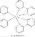
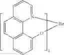
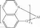
One example of a green emissive molecule is tris(2-phenylpyridine) iridium, denoted Ir(ppy)3, which has the following structure:
In this, and later figures herein, we depict the dative bond from nitrogen to metal (here, Ir) as a straight line.
As used herein, the term “organic” includes polymeric materials as well as small molecule organic materials that may be used to fabricate organic opto-electronic devices. “Small molecule” refers to any organic material that is not a polymer, and “small molecules” may actually be quite large. Small molecules may include repeat units in some circumstances. For example, using a long chain alkyl group as a substituent does not remove a molecule from the “small molecule” class. Small molecules may also be incorporated into polymers, for example as a pendent group on a polymer backbone or as a part of the backbone. Small molecules may also serve as the core moiety of a dendrimer, which consists of a series of chemical shells built on the core moiety. The core moiety of a dendrimer may be a fluorescent or phosphorescent small molecule emitter. A dendrimer may be a “small molecule,” and it is believed that all dendrimers currently used in the field of OLEDs are small molecules.
As used herein, “top” means furthest away from the substrate, while “bottom” means closest to the substrate. Where a first layer is described as “disposed over” a second layer, the first layer is disposed further away from substrate. There may be other layers between the first and second layer, unless it is specified that the first layer is “in contact with” the second layer. For example, a cathode may be described as “disposed over” an anode, even though there are various organic layers in between.
As used herein, “solution processible” means capable of being dissolved, dispersed, or transported in and/or deposited from a liquid medium, either in solution or suspension form.
A ligand may be referred to as “photoactive” when it is believed that the ligand directly contributes to the photoactive properties of an emissive material. A ligand may be referred to as “ancillary” when it is believed that the ligand does not contribute to the photoactive properties of an emissive material, although an ancillary ligand may alter the properties of a photoactive ligand.
As used herein, and as would be generally understood by one skilled in the art, a first “Highest Occupied Molecular Orbital” (HOMO) or “Lowest Unoccupied Molecular Orbital” (LUMO) energy level is “greater than” or “higher than” a second HOMO or LUMO energy level if the first energy level is closer to the vacuum energy level. Since ionization potentials (IP) are measured as a negative energy relative to a vacuum level, a higher HOMO energy level corresponds to an IP having a smaller absolute value (an IP that is less negative). Similarly, a higher LUMO energy level corresponds to an electron affinity (EA) having a smaller absolute value (an EA that is less negative). On a conventional energy level diagram, with the vacuum level at the top, the LUMO energy level of a material is higher than the HOMO energy level of the same material. A “higher” HOMO or LUMO energy level appears closer to the top of such a diagram than a “lower” HOMO or LUMO energy level.
As used herein, and as would be generally understood by one skilled in the art, a first work function is “greater than” or “higher than” a second work function if the first work function has a higher absolute value. Because work functions are generally measured as negative numbers relative to vacuum level, this means that a “higher” work function is more negative. On a conventional energy level diagram, with the vacuum level at the top, a “higher” work function is illustrated as further away from the vacuum level in the downward direction. Thus, the definitions of HOMO and LUMO energy levels follow a different convention than work functions.
More details on OLEDs, and the definitions described above, can be found in U.S. Pat. No. 7,279,704, which is incorporated herein by reference in its entirety.
SUMMARY OF THE INVENTION
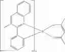
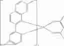
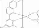
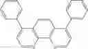
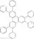
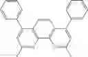
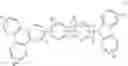
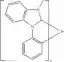
According to an embodiment of the present disclosure, a compound or a composition comprising such a compound is provided. The compound comprises triphenylene, carbazole and at least one spacer linkage between triphenylene and carbazole. The compound provided in the present disclosure has a general structure of the formula I:
wherein R1, R2, R3, R4, R5 and R6 each represent mono, di, tri, tetra substitutions, or no substitution, R9 represents mono, di, tri substitutions, or no substitution, R1, R2, R3, R4, R5, R6 and R9 are each independently selected from the group consisting of hydrogen, deuterium, halide, alkyl, cycloalkyl, heteroalkyl, arylalkyl, alkoxy, aryloxy, amino, silyl, alkenyl, cycloalkenyl, heteroalkenyl, alkynyl, aryl, heteroaryl, acyl, carbonyl, carboxylic acid, ester, nitrile, isonitrile, sulfanyl, sulfinyl, sulfonyl, phosphino, and combinations thereof. A1, A2, A3, A4, A5, and A6 are each independently selected from N or C and n is an integer from 1 to 20.
According to another embodiment of the present disclosure, a first device comprising an organic light-emitting device is provided. The first device comprises an anode, a cathode, and an organic layer. The organic layer is disposed between the anode and the cathode, and comprises a compound having formula I or a composition comprising a compound having formula I. The compound can be used alone or in combination of other materials in the organic layer for different functions. For example, in some embodiments, the organic layer is an emissive layer and the compound of the formula I is a host material. The compound of the formula I can be also used as a blocking material or an electron transporting material. The first device can be a consumer product, an organic light-emitting device, and/or a lighting panel.
BRIEF DESCRIPTION OF THE DRAWINGS
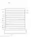
FIG. 1 shows an organic light emitting device.
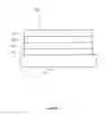
FIG. 2 shows an inverted organic light emitting device that does not have a separate electron transport layer.
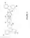
FIG. 3 shows Formula I as disclosed herein.
DETAILED DESCRIPTION
Generally, an OLED comprises at least one organic layer disposed between and electrically connected to an anode and a cathode. When a current is applied, the anode injects holes and the cathode injects electrons into the organic layer(s). The injected holes and electrons each migrate toward the oppositely charged electrode. When an electron and hole localize on the same molecule, an “exciton,” which is a localized electron-hole pair having an excited energy state, is formed, light is emitted when the exciton relaxes via a photoemissive mechanism. In some cases, the exciton may be localized on an excimer or an exciplex. Non-radiative mechanisms, such as thermal relaxation, may also occur, but are generally considered undesirable.
The initial OLEDs used emissive molecules that emitted light from their singlet states (“fluorescence”) as disclosed, for example, in U.S. Pat. No. 4,769,292, which is incorporated by reference in its entirety. Fluorescent emission generally occurs in a time frame of less than 10 nanoseconds.
More recently, OLEDs having emissive materials that emit light from triplet states (“phosphorescence”) have been demonstrated. Baldo et al., “Highly Efficient Phosphorescent Emission from Organic Electroluminescent Devices,” Nature, vol. 395, 151-154, 1998; (“Baldo-I”) and Baldo et al., “Very high-efficiency green organic light-emitting devices based on electrophosphorescence,” Appl. Phys. Lett., vol. 75, No. 3, 4-6 (1999) (“Baldo-II”), which are incorporated by reference in their entireties. Phosphorescence is described in more detail in U.S. Pat. No. 7,279,704 at cols. 5-6, which are incorporated by reference.
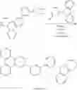
FIG. 1 shows an organic light emitting device 100. The figures are not necessarily drawn to scale. Device 100 may include a substrate 110, an anode 115, a hole injection layer 120, a hole transport layer 125, an electron blocking layer 130, an emissive layer 135, a hole blocking layer 140, an electron transport layer 145, an electron injection layer 150, a protective layer 155, a cathode 160, and a barrier layer 170. Cathode 160 can be a compound cathode having a first conductive layer 162 and a second conductive layer 164. Device 100 may be fabricated by depositing the layers described, in order. The properties and functions of these various layers, as well as example materials, are described in more detail in U.S. Pat. No. 7,279,704 at cols. 6-10, which are incorporated by reference.
More examples for each of these layers are available. For example, a flexible and transparent substrate-anode combination is disclosed in U.S. Pat. No. 5,844,363, which is incorporated by reference in its entirety. An example of a p-doped hole transport layer is m-MTDATA doped with F4-TCNQ at a molar ratio of 50:1, as disclosed in U.S. Patent Application Publication No, 2003/0230980, which is incorporated by reference in its entirety. Examples of emissive and host materials are disclosed in U.S. Pat. No. 6,303,238 to Thompson et al., which is incorporated by reference in its entirety. An example of an n-doped electron transport layer is BPhen doped with Li at a molar ratio of 1:1, as disclosed in U.S. Patent Application Publication No. 2003/0230980, which is incorporated by reference in its entirety. U.S. Pat. Nos. 5,703,436 and 5,707,745, which are incorporated by reference in their entireties, disclose examples of cathodes including compound cathodes having a thin layer of metal such as Mg:Ag with an overlying transparent, electrically-conductive, sputter-deposited ITO layer. The theory and use of blocking layers is described in more detail in U.S. Pat. No. 6,097,147 and U.S. Patent Application Publication No. 2003/0230980, which are incorporated by reference in their entireties. Examples of injection layers are provided in U.S. Patent Application Publication No. 2004/0174116, which is incorporated by reference in its entirety. A description of protective layers may be found in U.S. Patent Application Publication No. 2004/0174116, which is incorporated by reference in its entirety.
FIG. 2 shows an inverted OLED 200. The device includes a substrate 210, a cathode 215, an emissive layer 220, a hole transport layer 225, and an anode 230. Device 200 may be fabricated by depositing the layers described, in order. Because the most common OLED configuration has a cathode disposed over the anode, and device 200 has cathode 215 disposed under anode 230, device 200 may be referred to as an “inverted” OLED. Materials similar to those described with respect to device 100 may be used in the corresponding layers of device 200. FIG. 2 provides one example of how some layers may be omitted from the structure of device 100.
The simple layered structure illustrated in FIGS. 1 and 2 is provided by way of non-limiting example, and it is understood that embodiments of the invention may be used in connection with a wide variety of other structures. The specific materials and structures described are exemplary in nature, and other materials and structures may be used. Functional OLEDs may be achieved by combining the various layers described in different ways, or layers may be omitted entirely, based on design, performance, and cost factors. Other layers not specifically described may also be included. Materials other than those specifically described may be used. Although many of the examples provided herein describe various layers as comprising a single material, it is understood that combinations of materials, such as a mixture of host and dopant, or more generally a mixture, may be used. Also, the layers may have various sublayers. The names given to the various layers herein are not intended to be strictly limiting. For example, in device 200, hole transport layer 225 transports holes and injects holes into emissive layer 220, and may be described as a hole transport layer or a hole injection layer. In one embodiment, an OLED may be described as having an “organic layer” disposed between a cathode and an anode. This organic layer may comprise a single layer, or may further comprise multiple layers of different organic materials as described, for example, with respect to FIGS. 1 and 2.
Structures and materials not specifically described may also be used, such as OLEDs comprised of polymeric materials (PLEDs) such as disclosed in U.S. Pat. No. 5,247,190 to Friend et al., which is incorporated by reference in its entirety. By way of further example, OLEDs having a single organic layer may be used. OLEDs may be stacked, for example as described in U.S. Pat. No. 5,707,745 to Forrest et al, which is incorporated by reference in its entirety. The OLED structure may deviate from the simple layered structure illustrated in FIGS. 1 and 2. For example, the substrate may include an angled reflective surface to improve out-coupling, such as a mesa structure as described in U.S. Pat. No. 6,091,195 to Forrest et al., and/or a pit structure as described in U.S. Pat. No. 5,834,893 to Bulovic et al., which are incorporated by reference in their entireties.
Unless otherwise specified, any of the layers of the various embodiments may be deposited by any suitable method. For the organic layers, preferred methods include thermal evaporation, ink-jet, such as described in U.S. Pat. Nos. 6,013,982 and 6,087,196, which are incorporated by reference in their entireties, organic vapor phase deposition (OVPD), such as described in U.S. Pat. No. 6,337,102 to Forrest et al., which is incorporated by reference in its entirety, and deposition by organic vapor jet printing (OVJP), such as described in U.S. Pat. No. 7,431,968, which is incorporated by reference in its entirety. Other suitable deposition methods include spin coating and other solution based processes. Solution based processes are preferably carried out in nitrogen or an inert atmosphere. For the other layers, preferred methods include thermal evaporation. Preferred patterning methods include deposition through a mask, cold welding such as described in U.S. Pat. Nos. 6,294,398 and 6,468,819, which are incorporated by reference in their entireties, and patterning associated with some of the deposition methods such as ink-jet and OVJD. Other methods may also be used. The materials to be deposited may be modified to make them compatible with a particular deposition method. For example, substituents such as alkyl and aryl groups, branched or unbranched, and preferably containing at least 3 carbons, may be used in small molecules to enhance their ability to undergo solution processing. Substituents having 20 carbons or more may be used, and 3-20 carbons is a preferred range. Materials with asymmetric structures may have better solution processibility than those having symmetric structures, because asymmetric materials may have a lower tendency to recrystallize. Dendrimer substituents may be used to enhance the ability of small molecules to undergo solution processing.
Devices fabricated in accordance with embodiments of the present invention may further optionally comprise a barrier layer. One purpose of the barrier layer is to protect the electrodes and organic layers from damaging exposure to harmful species in the environment including moisture, vapor and/or gases, etc. The barrier layer may be deposited over, under or next to a substrate, an electrode, or over any other parts of a device including an edge. The barrier layer may comprise a single layer, or multiple layers. The barrier layer may be formed by various known chemical vapor deposition techniques and may include compositions having a single phase as well as compositions having multiple phases. Any suitable material or combination of materials may be used for the barrier layer. The barrier layer may incorporate an inorganic or an organic compound or both. The preferred barrier layer comprises a mixture of a polymeric material and a non-polymeric material as described in U.S. Pat. No. 7,968,146, PCT Pat. Application Nos. PCT/US2007/023098 and PCT/US2009/042829, which are herein incorporated by reference in their entireties. To be considered a “mixture”, the aforesaid polymeric and non-polymeric materials comprising the barrier layer should be deposited under the same reaction conditions and/or at the same time. The weight ratio of polymeric to non-polymeric material may be in the range of 95:5 to 5:95. The polymeric material and the non-polymeric material may be created from the same precursor material. In one example, the mixture of a polymeric material and a non-polymeric material consists essentially of polymeric silicon and inorganic silicon.
Devices fabricated in accordance with embodiments of the invention may be incorporated into a wide variety of consumer products, including flat panel displays, computer monitors, medical monitors, televisions, billboards, lights for interior or exterior illumination and/or signaling, heads up displays, fully transparent displays, flexible displays, laser printers, telephones, cell phones, personal digital assistants (PDAs), laptop computers, digital cameras, camcorders, viewfinders, micro-displays, vehicles, a large area wall, theater or stadium screen, or a sign. Various control mechanisms may be used to control devices fabricated in accordance with the present invention, including passive matrix and active matrix. Many of the devices are intended for use in a temperature range comfortable to humans, such as 18 degrees C. to 30 degrees C., and more preferably at room temperature (20-25 degrees C.).
The materials and structures described herein may have applications in devices other than OLEDs. For example, other optoelectronic devices such as organic solar cells and organic photodetectors may employ the materials and structures. More generally, organic devices, such as organic transistors, may employ the materials and structures.
The terms for chemical substitution groups such as halo, halogen, alkyl, cycloalkyl, alkenyl, alkynyl, arylkyl, heterocyclic group, aryl, aromatic group, and heteroaryl are known to the art, and are defined in U.S. Pat. No. 7,279,704 at cols. 31-32, which are incorporated herein by reference.
In the chemical formulas in the present disclosure, either a solid line or a dotted line represents a chemical bond or multiple chemical bonds. Unless expressly stated otherwise, the solid lines and the dotted lines do not represent spatial arrangements of chemical bonds in stereochemistry. A solid line or a dotted line across a chemical structure such as a ring or a fused ring represents either one chemical bond or multiple bonds connected with one or multiple possible positions of the chemical structure.
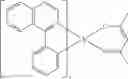
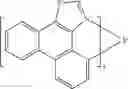
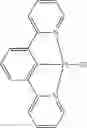
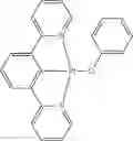
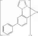
Triphenylene containing compounds provide excellent stability in phosphorescent OLEDs (PHOLEDs). Carbazole containing compounds have been used as host materials in the emissive layers in PHOLEDs. 4,4′-di(9H-carbazol-9-yl)-1,1′-biphenyl (CBP) is a commonly used carbazole containing host for green PHOLEDs. However, the lifetime of the devices that use CBP as a host does not meet commercial requirements. It has been found that carbazole can undergo oxidative coupling to form bicarbazole when it is oxidized. This instability of carbazole to positive charges may translate into the poor device lifetime of PHOLEDs that contain carbazole group in the host material.
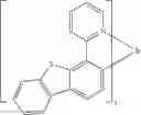
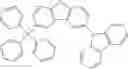
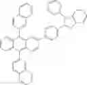
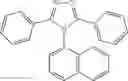
According to an embodiment of the present disclosure, a compound or a composition comprising a compound that comprises triphenylene, carbazole and at least one spacer linkage between triphenylene and carbazole is disclosed as a host material for PHOLEDs that enhances the lifetime of PHOLEDs. As shown in FIG. 3, the compound has a general structure of the formula I:
wherein R1, R2, R3, R4, R5 and R6 each represent mono, di, tri, tetra substitutions, or no substitution. R9 represents mono, di, tri substitutions, or no substitution. R1, R2, R3, R4, R5, R6 and R9 are each independently selected from the group consisting of hydrogen, deuterium, halide, alkyl, cycloalkyl, heteroalkyl, arylalkyl, alkoxy, aryloxy, amino, silyl, alkenyl, cycloalkenyl, heteroalkenyl, alkynyl, aryl, heteroaryl, acyl, carbonyl, carboxylic acid, ester, nitrile, isonitrile, sulfanyl, sulfinyl, sulfonyl, phosphino, and combinations thereof. A1, A2, A3, A4, A5, and A6 are each independently selected from N or C and n is an integer from 1 to 20.
Combining the triphenylene group and carbazole group in a host compound would not be expected to solve the oxidation problem because triphenylene is even harder to oxidize. However, the inventors have unexpectedly discovered that the combination of triphenylene and carbazole in certain manners in a host compound can improve PHOLEDs' device lifetime. Without being bound by any theory, the inventors believe that this unexpected improvement may be related to solid state packing and charge transport properties.
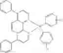
In some embodiments, the compound provided in the present disclosure has the formula II, III, IV or V:
wherein the substitution groups are the same as described in the formula I.
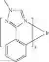
In some embodiments, the compound provided in the present disclosure has the formula VI:
wherein R7 and R8 are each independently selected from the group consisting of hydrogen, deuterium, halide, alkyl, cycloalkyl, heteroalkyl, arylalkyl, alkoxy, aryloxy, amino, silyl, alkenyl, cycloalkenyl, heteroalkenyl, alkynyl, aryl, heteroaryl, acyl, carbonyl, carboxylic acid, ester, nitrile, isonitrile, sulfanyl, sulfinyl, sulfonyl, phosphino, and combinations thereof. Other groups are the same as described in the formula I.
In some embodiments, the functional groups of R1, R2, R3, R4, R5, R6 and R9 in the formulas I, II, III, IV, V and VI are each independently selected from the group consisting of hydrogen, deuterium, silyl, aryl, and heteroaryl.
In some embodiments, the compound provided in the present disclosure has the formula VII:
wherein the substitution groups are the same as described in the formula I, and n is an integer from 1 to 5.
In some embodiments, in the compound having the formula VII, n is an integer from 1 to 3 and R1, R2, R3, R4, R5, R6 and R9 are each independently selected from the group consisting of hydrogen and phenyl. For example, n is 1 and R1, R2, R3, R4, R5, R6 and R9 are hydrogen.
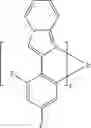
In some embodiments, in a compound provided in this disclosure, at least one of A1, A2, A3, A4, A5, and A6 is N (nitrogen). The compound has the general formula VIII or IX:
wherein the substitution groups are the same as described in the formula I and n is an integer from 1 to 5.
In some embodiments, in the compound having the formula VIII or IX, n is an integer from 1 to 3 and R1, R2, R3, R4, R5, R6 and R9 are each independently selected from the group consisting of hydrogen and phenyl. For example, n is equal to two in some embodiments.
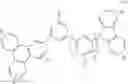
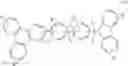
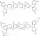
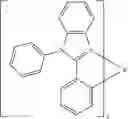
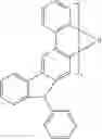
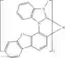
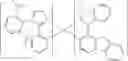
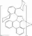
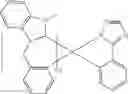
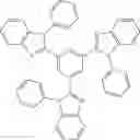
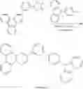
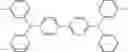
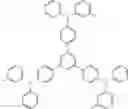
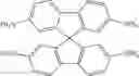
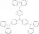
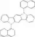
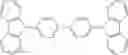
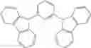
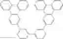
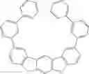
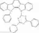
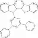
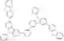
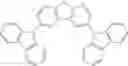
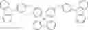
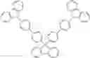
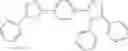
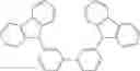
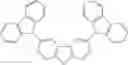
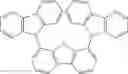
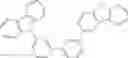
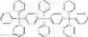
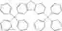
In some embodiments, examples of compounds having the formula I include but are not limited to the following compounds (compounds 1-53):
A composition comprising a compound represented by the formula I described above is also provided in the present disclosure. Such composition can be formulated with other materials suitable for organic light emitting applications. Examples of other suitable materials include but are not limited to a host compound, a phosphorescent dopant, a blocking material, an electron transporting material, an additive, and any combination thereof. Examples of compounds having the formula I can have general structures as described in the formulas I-IX. Examples of a suitable exemplary compound include but are not limited to the following compound (compounds 1-53) described above.
According to an embodiment of the present disclosure, a first device comprising the organic light-emitting device is provided. The OLED comprises an anode, a cathode, and an organic layer disposed between the anode and the cathode. The organic layer comprises a compound having the formula I or a composition comprising a compound having the formula I.
The compound can be used alone or in combination with other materials in the organic layer for different functions. For example, the compound having the formula I can be also used as a blocking material or an electron transporting material. The first device can be a consumer product, an organic light-emitting device, and/or a lighting panel.
According to the present disclosure, the compounds provided in the present disclosure give good results in green PHOLEDs as a host material in the emissive layer. In addition, the compounds are soluble in organic solvents such as toluene. Solution process can be used to be fabricated high performance PHOLED.
Combination with Other Materials
The materials described herein as useful for a particular layer in an organic light emitting device may be used in combination with a wide variety of other materials present in the device. For example, emissive dopants disclosed herein may be used in conjunction with a wide variety of hosts, transport layers, blocking layers, injection layers, electrodes and other layers that may be present. The materials described or referred to below are non-limiting examples of materials that may be useful in combination with the compounds disclosed herein, and one of skill in the art can readily consult the literature to identify other materials that may be useful in combination.
HIL/HTL:
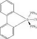
A hole injecting/transporting material to be used in the present invention is not particularly limited, and any compound may be used as long as the compound is typically used as a hole injecting/transporting material. Examples of the material include, but not limit to: a phthalocyanine or porphryin derivative; an aromatic amine derivative; an indolocarbazole derivative; a polymer containing fluorohydrocarbon; a polymer with conductivity dopants; a conducting polymer, such as PEDOT/PSS; a self-assembly monomer derived from compounds such as phosphonic acid and sliane derivatives; a metal oxide derivative, such as MoOx; a p-type semiconducting organic compound, such as 1,4,5,8,9,12-Hexaazatriphenylenehexacarbonitrile; a metal complex, and a cross-linkable compounds.
Examples of aromatic amine derivatives used in HIL or HTL include, but not limit to the following general structures:
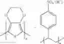
Each of Ar1 to Ar9 is selected from the group consisting aromatic hydrocarbon cyclic compounds such as benzene, biphenyl, triphenyl, triphenylene, naphthalene, anthracene, phenalene, phenanthrene, fluorene, pyrene, chrysene, perylene, azulene; group consisting aromatic heterocyclic compounds such as dibenzothiophene, dibenzofuran, dibenzoselenophene, furan, thiophene, benzofuran, benzothiophene, benzoselenophene, carbazole, indolocarbazole, pyridylindole, pyrrolodipyridine, pyrazole, imidazole, triazole, oxazole, thiazole, oxadiazole, oxatriazole, dioxazole, thiadiazole, pyridine, pyridazine, pyrimidine, pyrazine, triazine, oxazine, oxathiazine, oxadiazine, indole, benzimidazole, indazole, indoxazine, benzoxazole, benzisoxazole, benzothiazole, quinoline, isoquinoline, cinnoline, quinazoline, quinoxaline, naphthyridine, phthalazine, pteridine, xanthene, acridine, phenazine, phenothiazine, phenoxazine, benzofuropyridine, furodipyridine, benzothienopyridine, thienodipyridine, benzoselenophenopyridine, and selenophenodipyridine; and group consisting 2 to 10 cyclic structural units which are groups of the same type or different types selected from the aromatic hydrocarbon cyclic group and the aromatic heterocyclic group and are bonded to each other directly or via at least one of oxygen atom, nitrogen atom, sulfur atom, silicon atom, phosphorus atom, boron atom, chain structural unit and the aliphatic cyclic group. Wherein each Ar is further substituted by a substituent selected from the group consisting of hydrogen, deuterium, halide, alkyl, cycloalkyl, heteroalkyl, arylalkyl, alkoxy, aryloxy, amino, silyl, alkenyl, cycloalkenyl, heteroalkenyl, alkynyl, aryl, heteroaryl, acyl, carbonyl, carboxylic acids, ester, nitrile, isonitrile, sulfanyl, sulfinyl, sulfonyl, phosphino, and combinations thereof.
In one aspect, Ar1 to Ar9 is independently selected from the group consisting of:
where k is an integer from 1 to 20; X101 to X108 is C (including CH) or N; Z101 is NAr1, O, or S; Ar1 has the same group defined above.
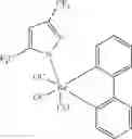
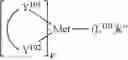
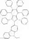
Examples of metal complexes used in HIL or HTL include, but not limit to the following general formula:
where Met is a metal; (Y101-Y102) is a bidentate ligand, Y101 and Y102 are independently selected from C, N, O, P, and S, L101 is another ligand, k′ is an integer value from 1 to the maximum number of ligands that may be attached to the metal, and k′+k″ is the maximum number of ligands that may be attached to the metal.
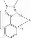
In one aspect, (Y101-Y102) is a 2-phenylpyridine derivative.
In another aspect, (Y101-Y102) is a carbene ligand.
In another aspect, Met is selected from Ir, Pt, Os, and Zn.
In a further aspect, the metal complex has a smallest oxidation potential in solution vs. Fc+/Fc couple less than about 0.6 V.
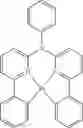
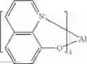
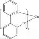
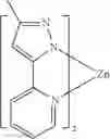
Host:
The light emitting layer of the organic EL device of the present invention preferably contains at least a metal complex as light emitting material, and may contain a host material using the metal complex as a dopant material. Examples of the host material are not particularly limited, and any metal complexes or organic compounds may be used as long as the triplet energy of the host is larger than that of the dopant. While the Table 1 below categorizes host materials as preferred for devices that emit various colors, any host material may be used with any dopant so long as the triplet criteria is satisfied.
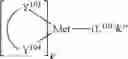
Examples of metal complexes used as host are preferred to have the following general formula:
Met is a metal; (Y103-Y104) is a bidentate ligand, Y103 and Y104 are independently selected from C, N, O, P, and S; L101 is an another ligand; k′ is an integer value from 1 to the maximum number of ligands that may be attached to the metal; and k′+k″ is the maximum number of ligands that may be attached to the metal.
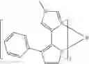
In one aspect, the metal complexes are:
(O—N) is a bidentate ligand, having metal coordinated to atoms O and N.
In another aspect, Met is selected from Ir and Pt.
In a further aspect, (Y103-Y104) is a carbene ligand.
Examples of organic compounds used as host are selected from the group consisting aromatic hydrocarbon cyclic compounds such as benzene, biphenyl, triphenyl, triphenylene, naphthalene, anthracene, phenalene, phenanthrene, fluorene, pyrene, chrysene, perylene, azulene; group consisting aromatic heterocyclic compounds such as dibenzothiophene, dibenzofuran, dibenzoselenophene, furan, thiophene, benzofuran, benzothiophene, benzoselenophene, carbazole, indolocarbazole, pyridylindole, pyrrolodipyridine, pyrazole, imidazole, triazole, oxazole, thiazole, oxadiazole, oxatriazole, dioxazole, thiadiazole, pyridine, pyridazine, pyrimidine, pyrazine, triazine, oxazine, oxathiazine, oxadiazine, indole, benzimidazole, indazole, indoxazine, benzoxazole, benzisoxazole, benzothiazole, quinoline, isoquinoline, cinnoline, quinazoline, quinoxaline, naphthyridine, phthalazine, pteridine, xanthene, acridine, phenazine, phenothiazine, phenoxazine, benzofuropyridine, furodipyridine, benzothienopyridine, thienodipyridine, benzoselenophenopyridine, and selenophenodipyridine; and group consisting 2 to 10 cyclic structural units which are groups of the same type or different types selected from the aromatic hydrocarbon cyclic group and the aromatic heterocyclic group and are bonded to each other directly or via at least one of oxygen atom, nitrogen atome, sulfur atom, silicon atom, phosphorus atom, boron atom, chain structural unit and the aliphatic cyclic group. Wherein each group is further substituted by a substituent selected from the group consisting of hydrogen, deuterium, halide, alkyl, cycloalkyl, heteroalkyl, arylalkyl, alkoxy, aryloxy, amino, silyl, alkenyl, cycloalkenyl, heteroalkenyl, alkynyl, aryl, heteroaryl, acyl, carbonyl, carboxylic acids, ester, nitrile, isonitrile, sulfanyl, sulfinyl, sulfonyl, phosphino, and combinations thereof.
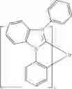
In one aspect, host compound contains at least one of the following groups in the molecule:
where R101 to R107 is independently selected from the group consisting of hydrogen, deuterium, halide, alkyl, cycloalkyl, heteroalkyl, arylalkyl, alkoxy, aryloxy, amino, silyl, alkenyl, cycloalkenyl, heteroalkenyl, alkynyl, aryl, heteroaryl, acyl, carbonyl, carboxylic acids, ester, nitrile, isonitrile, sulfanyl, sulfinyl, sulfonyl, phosphino, and combinations thereof, when it is aryl or heteroaryl, it has the similar definition as Ar's mentioned above.
k is an integer from 1 to 20; k′″ is an integer from 0 to 20.
X101 to X108 is selected from C (including CH) or N.
Z101 and Z102 is selected from NR101, O, or S.
HBL:
A hole blocking layer (HBL) may be used to reduce the number of holes and/or excitons that leave the emissive layer. The presence of such a blocking layer in a device may result in substantially higher efficiencies as compared to a similar device lacking a blocking layer. Also, a blocking layer may be used to confine emission to a desired region of an OLED.
In one aspect, compound used in HBL contains the same molecule or the same functional groups used as host described above.
In another aspect, compound used in HBL contains at least one of the following groups in the molecule:
where k is an integer from 1 to 20; L101 is an another ligand, k′ is an integer from 1 to 3.
ETL:
Electron transport layer (ETL) may include a material capable of transporting electrons. Electron transport layer may be intrinsic (undoped), or doped. Doping may be used to enhance conductivity. Examples of the ETL material are not particularly limited, and any metal complexes or organic compounds may be used as long as they are typically used to transport electrons.
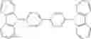
In one aspect, compound used in ETL contains at least one of the following groups in the molecule:
R101 is selected from the group consisting of hydrogen, deuterium, halide, alkyl, cycloalkyl, heteroalkyl, arylalkyl, alkoxy, aryloxy, amino, silyl, alkenyl, cycloalkenyl, heteroalkenyl, alkynyl, aryl, heteroaryl, acyl, carbonyl, carboxylic acids, ester, nitrile, isonitrile, sulfanyl, sulfinyl, sulfonyl, phosphino, and combinations thereof, when it is aryl or heteroaryl, it has the similar definition as Ar's mentioned above.
Ar1 to Ar3 has the similar definition as Ar's mentioned above.
k is an integer from 1 to 20.
X101 to X108 is selected from C (including CH) or N.
In another aspect, the metal complexes used in ETL contains, but not limit to the following general formula:
(O—N) or (N—N) is a bidentate ligand, having metal coordinated to atoms O, N or N, N; L101 is another ligand; k′ is an integer value from 1 to the maximum number of ligands that may be attached to the metal.
In any above-mentioned compounds used in each layer of the OLED device, the hydrogen atoms can be partially or fully deuterated. Thus, any specifically listed substituent, such as, without limitation, methyl, phenyl, pyridyl, etc. encompasses undeuterated, partially deuterated, and fully deuterated versions thereof. Similarly, classes of substituents such as, without limitation, alkyl, aryl, cycloalkyl, heteroaryl, etc. also encompass undeuterated, partially deuterated, and fully deuterated versions thereof.
In addition to and/or in combination with the materials disclosed herein, many hole injection materials, hole transporting materials, host materials, dopant materials, exiton/hole blocking layer materials, electron transporting and electron injecting materials may be used in an OLED. Non-limiting examples of the materials that may be used in an OLED in combination with materials disclosed herein are listed in Table 1 below. Table 1 lists non-limiting classes of materials, non-limiting examples of compounds for each class, and references that disclose the materials.
| TABLE 1 | ||
| MATERIAL | EXAMPLES OF MATERIAL | PUBLICATIONS |
| Hole injection materials |
| Phthalocyanine and porphryin compounds | Appl. Phys. Lett. 69, 2160 (1996) | |
| Starburst triarylamines | J. Lumin. 72-74, 985 (1997) | |
| CFx Fluorohydrocarbon polymer | Appl. Phys. Lett. 78, 673 (2001) | |
| Conducting polymers (e.g., PEDOT:PSS, polyaniline, polypthiophene) | Synth. Met. 87, 171 (1997) WO2007002683 | |
| Phosphonic acid and sliane SAMs | US20030162053 | |
| Triarylamine or polythiophene polymers with conductivity dopants | EP1725079A1 | |
| Organic compounds with conductive inorganic compounds, such as molybdenum and tungsten oxides | US20050123751 SID Symposium Digest, 37, 923 (2006) WO2009018009 | |
| n-type semiconducting | US20020158242 | |
| organic complexes | ||
| Metal organometallic | US20060240279 | |
| complexes | ||
| Cross-linkable compounds | US20080220265 | |
| Polythiophene based | WO 2011075644 | |
| polymers and copolymers | EP2350216 |
| Hole transporting materials |
| Triarylamines (e.g., TPD, α-NPD) | Appl. Phys. Lett. 51, 913 (1987) | |
| US5061569 | ||
| EP650955 | ||
| J. Mater. Chem. 3, 319 (1993) | ||
| Appl. Phys. Lett. 90, 183503 (2007) | ||
| Appl. Phys. Lett. 90, 183503 (2007) | ||
| Triaylamine on spirofluorene core | Synth. Met. 91, 209 (1997) | |
| Arylamine carbazole compounds | Adv. Mater. 6, 677 (1994), US20080124572 | |
| Triarylamine with (di)benzothiophene/(di)ben zofuran | US20070278938, US20080106190 US20110163302 | |
| Indolocarbazoles | Synth. Met. 111, 421 (2000) | |
| Isoindole compounds | Chem. Mater. 15, 3148 (2003) | |
| Metal carbene complexes | US20080018221 | |
| Phosphorescent OLED host materials |
| Red hosts |
| Arylcarbazoles | Appl. Phys. Lett. 78, 1622 (2001) | |
| Metal 8-hydroxyquinolates (e.g., Alq3, BAlq) | Nature 395, 151 (1998) | |
| US20060202194 | ||
| WO2005014551 | ||
| WO2006072002 | ||
| Metal phenoxybenzothiazole compounds | Appl. Phys. Lett. 90, 123509 (2007) | |
| Conjugated oligomers and polymers (e.g., polyfluorene) | Org. Electron. 1, 15 (2000) | |
| Aromatic fused rings | WO2009066779, WO2009066778, WO2009063833, US20090045731, US20090045730, WO2009008311, US20090008605, US20090009065 | |
| Zinc complexes | WO2010056066 | |
| Chrysene based compounds | WO2011086863 | |
| Green hosts |
| Arylcarbazoles | Appl. Phys. Lett. 78, 1622 (2001) | |
| US20030175553 | ||
| WO2001039234 | ||
| Aryltriphenylene compounds | US20060280965 | |
| US20060280965 | ||
| WO2009021126 | ||
| Poly-fused heteroaryl compounds | US20090309488 US20090302743 US20100012931 | |
| Donor acceptor type molecules | WO2008056746 | |
| WO2010107244 | ||
| Aza-carbazole/DBT/DBF | JP2008074939 | |
| US20100187984 | ||
| Polymers (e.g., PVK) | Appl. Phys. Lett. 77, 2280 (2000) | |
| Spirofluorene compounds | WO2004093207 | |
| Metal phenoxybenzooxazole compounds | WO2005089025 | |
| WO2006132173 | ||
| JP200511610 | ||
| Spirofluorene-carbazole compounds | JP2007254297 | |
| JP2007254297 | ||
| Indolocabazoles | WO2007063796 | |
| WO2007063754 | ||
| 5-member ring electron deficient heterocycles (e.g., triazole, oxadiazole) | J. Appl. Phys. 90, 5048 (2001) | |
| WO2004107822 | ||
| Tetraphenylene complexes | US20050112407 | |
| Metal phenoxypyridine compounds | WO2005030900 | |
| Metal coordination complexes (e.g., Zn, Al with N{circumflex over ( )}N ligands) | US20040137268, US20040137267 | |
| Blue hosts |
| Arylcarbazoles | Appl. Phys. Lett, 82, 2422 (2003) | |
| US20070190359 | ||
| Dibenzothiophene/Dibenz ofuran-carbazole compounds | WO2006114966, US20090167162 | |
| US20090167162 | ||
| WO2009086028 | ||
| US20090030202, US20090017330 | ||
| US20100084966 | ||
| Silicon aryl compounds | US20050238919 | |
| WO2009003898 | ||
| Silicon/Germanium aryl compounds | EP2034538A | |
| Aryl benzoyl ester | WO2006100298 | |
| Carbazole linked by non- conjugated groups | US20040115476 | |
| Aza-carbazoles | US20060121308 | |
| High triplet metal organometallic complex | US7154114 | |
| Phosphorescent dopants |
| Red dopants |
| Heavy metal porphyrins (e.g., PtOEP) | Nature 395, 151 (1998) | |
| Iridium(III) organometallic complexes | Appl. Phys. Lett. 78, 1622 (2001) | |
| US2006835469 | ||
| US2006835469 | ||
| US20060202194 | ||
| US20060202194 | ||
| US20070087321 | ||
| US20080261076 US20100090591 | ||
| US20070087321 | ||
| Adv. Mater. 19, 739 (2007) | ||
| WO2009100991 | ||
| WO2008101842 | ||
| US7232618 | ||
| Platinum(II) organometallic complexes | WO2003040257 | |
| US20070103060 | ||
| Osminum(III) complexes | Chem. Mater. 17, 3532 (2005) | |
| Ruthenium(II) complexes | Adv. Mater. 17, 1059 (2005) | |
| Rhenium (I), (II), and (III) | US20050244673 | |
| complexes |
| Green dopants |
| Iridium(III) organometallic complexes | Inorg. Chem. 40, 1704 (2001) | |
| US20020034656 | ||
| US7332232 | ||
| US20090108737 | ||
| WO2010028151 | ||
| EP1841834B | ||
| US20060127696 | ||
| US20090039776 | ||
| US6921915 | ||
| US20100244004 | ||
| US6687266 | ||
| Chem. Mater. 16, 2480 (2004) | ||
| US20070190359 | ||
| US 20060008670 JP2007123392 | ||
| WO2010086089, WO2011044988 | ||
| Adv. Mater. 16, 2003 (2004) | ||
| Angew. Chem. Int. Ed. 2006, 45, 7800 | ||
| WO2009050290 | ||
| US20090165846 | ||
| US20080015355 | ||
| US20010015432 | ||
| US20100295032 | ||
| Monomer for polymeric metal organometallic compounds | US7250226, US7396598 | |
| Pt(II) organometallic complexes, including polydentated ligands | Appl. Phys. Lett. 86, 153505 (2005) | |
| Appl. Phys. Lett. 86, 153505 (2005) | ||
| Chem. Lett. 34, 592 (2005) | ||
| WO2002015645 | ||
| US20060263635 | ||
| US20060182992 US20070103060 | ||
| Cu complexes | WO2009000673 | |
| US20070111026 | ||
| Gold complexes | Chem. Commun. 2906 (2005) | |
| Rhenium(III) complexes | Inorg. Chem. 42, 1248 (2003) | |
| Osmium(II) complexes | US7279704 | |
| Deuterated organometallic | US20030138657 | |
| complexes | ||
| Organometallic complexes | US20030152802 | |
| with two or more metal | ||
| centers | ||
| US7090928 | ||
| Blue dopants |
| Iridium(III) organometallic complexes | WO2002002714 | |
| WO2006009024 | ||
| US20060251923 US20110057559 US20110204333 | ||
| US7393599, WO2006056418, US20050260441, WO2005019373 | ||
| US7534505 | ||
| WO2011051404 | ||
| US7445855 | ||
| US20070190359, US20080297033 US20100148663 | ||
| US7338722 | ||
| US20020134984 | ||
| Angew. Chem. Int. Ed. 47, 1 (2008) | ||
| Chem. Mater. 18, 5119 (2006) | ||
| Inorg. Chem. 46, 4308 (2007) | ||
| WO2005123873 | ||
| WO2005123873 | ||
| WO2007004380 | ||
| WO2006082742 | ||
| Osmium(II) complexes | US7279704 | |
| Organometallics 23, 3745 (2004) | ||
| Gold complexes | Appl. Phys. Lett. 74, 1361 (1999) | |
| Platinum(II) complexes | WO2006098120, WO2006103874 | |
| Pt tetradentate complexes with at least one metal- carbene bond | US7655323 | |
| Exciton/hole blocking layer materials |
| Bathocuprine compounds (e.g., BCP, BPhen) | Appl. Phys. Lett. 75, 4 (1999) | |
| Appl. Phys. Lett. 79, 449 (2001) | ||
| Metal 8-hydroxyquinolates (e.g., BAlq) | Appl. Phys. Lett. 81, 162 (2002) | |
| 5-member ring electron deficient heterocycles such as triazole, oxadiazole, imidazole, benzoimidazole | Appl. Phys. Lett. 81, 162 (2002) | |
| Triphenylene compounds | US20050025993 | |
| Fluorinated aromatic compounds | Appl. Phys. Lett. 79, 156 (2001) | |
| Phenothiazine-S-oxide | WO2008132085 | |
| Silylated five-membered nitrogen, oxygen, sulfur or phosphorus dibenzoheterocycles | WO2010079051 | |
| Aza-carbazoles | US20060121308 | |
| Electron transporting materials |
| Anthracene- benzoimidazole compounds | WO2003060956 | |
| US20090179554 | ||
| Aza triphenylene derivatives | US20090115316 | |
| Anthracene-benzothiazole compounds | Appl. Phys. Lett. 89, 063504 (2006) | |
| Metal 8-hydroxyquinolates (e.g., Alq3, Zrq4) | Appl. Phys. Lett. 51, 913 (1987) US7230107 | |
| Metal hydroxybenoquinolates | Chem. Lett. 5, 905 (1993) | |
| Bathocuprine compounds such as BCP, BPhen, etc | Appl. Phys. Lett. 91, 263503 (2007) | |
| Appl. Phys. Lett. 79, 449 (2001) | ||
| 5-member ring electron deficient heterocycles (e.g., triazole, oxadiazole, imidazole, benzoimidazole) | Appl. Phys. Lett. 74, 865 (1999) | |
| Appl. Phys. Lett. 55, 1489 (1989) | ||
| Jpn. J. Apply. Phys. 32, L917 (1993) | ||
| Silole compounds | Org. Electron. 4, 113 (2003) | |
| Arylborane compounds | J. Am. Chem. Soc. 120, 9714 (1998) | |
| Fluorinated aromatic compounds | J. Am. Chem. Soc. 122, 1832 (2000) | |
| Fullerene (e.g., C60) | US20090101870 | |
| Triazine complexes | US20040036077 | |
| Zn (N{circumflex over ( )}N) complexes | US6528187 | |
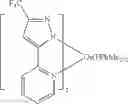
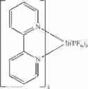
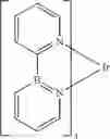
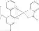
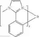
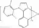
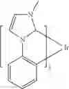
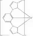
In some embodiments, the organic layer in the first device is an emissive layer and the compound of formula I is a host material. The organic layer may further comprise an emissive dopant. The emissive dopant is a transition metal complex having at least one ligand. Examples of the least one ligand include but are not limited to:
Wherein Ra, Rb, and Rc may represent mono, di, tri or tetra substitutions, Ra, Rb, and Rc are independently selected from the group consisting of hydrogen, deuterium, halide, alkyl, cycloalkyl, heteroalkyl, arylalkyl, alkoxy, aryloxy, amino, silyl, alkenyl, cycloalkenyl, heteroalkenyl, alkynyl, aryl, heteroaryl, acyl, carbonyl, carboxylic acid, ester, nitrile, isonitrile, sulfanyl, sulfinyl, sulfonyl, phosphino, and combinations thereof, and two adjacent substituents of Ra, Rb, and Rc are optionally joined to form a fused ring.
Examples of the transition metal in the emissive dopant include but are not limited to Ir, Pt, Os, Ru, Au, Cu, and Re and combinations thereof.
EXPERIMENTAL
Synthesis of Compound 1
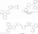
A solution of 9-(3-(4,4,5,5-tetramethyl-1,3,2-dioxaborolan-2-yl)phenyl)-9H-carbazole (5.0 g, 13.5 mmol), 2-(3-bromophenyl)triphenylene (4.2 g, 10.8 mmol), Pd2(dba)3 (0.20 g, 0.22 mmol), SPhos (0.36 g, 0.87 mmol) and K3PO4 (9.2 g, 43.3 mmol) in toluene (100 ml) and water (10 ml) was refluxed under nitrogen for 12 h. After cooling to room temperature, it was diluted with water and extracted with DCM. The combined organic extracts were washed with brine and dried over MgSO4. Upon evaporation off the solvent, the residue was purified by column chromatography on silica gel with hexane/DCM (9/1 to 7/1, v/v) as eluent. The crude product was redissolved in boiling toluene and filtered through a short plug of silica gel topped with MgSO4 to yield Compound 1 (2.5 g, 42%) as a white solid.
Synthesis of Compound 2
A solution of 4,4,5,5-tetramethyl-2-(3-(triphenylen-2-yl)phenyl)-1,3,2-dioxaborolane (3.6 g, 8.4 mmol), 9-(4-bromophenyl)-9H-carbazole (3.0 g, 9.2 mmol), Pd(PPh3)4 (0.19 g, 0.17 mmol) and K2CO3 (3.5 g, 25.1 mmol) in toluene (50 ml) and water (25 ml) was refluxed at 110° C. overnight. After cooling to room temperature, the organic phase was isolated and the aqueous phase was extracted with dichloromethane The combined organic solutions were washed with water and dried over MgSO4. Upon evaporation off the solvent, the residue was purified by column chromatography on silica gel with hexane/DCM (85/15 to 75/25, v/v) as eluent and the crude product was triturated with boiling ethyl acetate to yield Compound 2 (3.0 g, 66%) as a white solid.
Synthesis of Compound 5
A solution of 4,4,5,5-tetramethyl-2-(3-(triphenylen-2-yl)phenyl)-1,3,2-dioxaborolane (3.0 g, 7.0 mmol), 9-(3′-bromo-[1,1′-biphenyl]-3-yl)-9H-carbazole (2.8 g, 7.0 mmol), Pd(PPh3)4 (0.24 g, 0.21 mmol) and K2CO3 (2.9 g, 20.9 mmol) in toluene (45 ml) and water (15 ml) was refluxed under nitrogen overnight. After cooling to room temperature, the organic phase was isolated, and the aqueous phase was extracted with DCM. The combined organic extracts were washed with water and dried over MgSO4. Upon evaporation off the solvent, the residue was purified by column chromatography on silica gel with hexane/DCM (9/1 to 4/1, v/v) as eluent and precipitation in ethanol to yield Compound 5 (2.1 g, 48%) as a white solid.
Synthesis of Compound 53
A solution of 4,4,5,5-tetramethyl-2-(3-(triphenylen-2-yl)phenyl)-1,3,2-dioxaborolane (3.5 g, 8.1 mmol), 9-(6-bromopyridin-2-yl)-9H-carbazole (2.6 g, 8.1 mmol), Pd2(dba)3 (0.15 g, 0.16 mmol), SPhos (0.13 g, 0.33 mmol) and K3PO4 (5.2 g, 24.4 mmol) in toluene (100 ml) and water (25 ml) was refluxed at 110° C. under nitrogen overnight. After cooling to room temperature, it was diluted with water. The solid was collected by filtration and washed with large amount of water and ethanol, dissolved in boiling toluene (500 ml) and filtered through a short plug of silica gel. Upon evaporation off the solvent, the crude product was triturated with boiling ethyl acetate and cooled to room temperature to yield Compound 53 (3.5 g, 79%) as a white solid.
Device Examples
All devices were fabricated by high vacuum (˜10−7 Torr) thermal evaporation. The anode electrode was 120 nm of indium tin oxide (ITO). The cathode consisted of 1 nm of LiF followed by 100 nm of Aluminum. All devices were encapsulated with a glass lid sealed with an epoxy resin in a nitrogen glove box 1 ppm of H2O and O2) immediately after fabrication, and a moisture getter was incorporated inside the package.
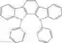
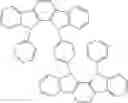
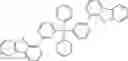
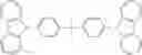
All device examples had organic stacks consisting of, sequentially, from the ITO surface, 10 nm thick of Compound A as the hole injection layer (HIL), 30 nm of 4,4′-bis[N-(1-naphthyl)-N-phenylamino]biphenyl (α-NPD), as the hole transporting layer (HTL), and 300 Å of inventive hosts or comparative hosts doped with 10 wt % of Compound A as the emissive layer (EML). On the top of the EML, 5 nm of Compound BL was deposited as a hole blocking (BL) and then followed by 45 nm of tris(8-hydroxyquinolinato)aluminum (Alq3) as the ETL. The comparative Examples were fabricated similarly to Device Example 1, except that Compounds B, C, D and CBP were used as the emitter in the EML, respectively.
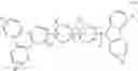
The device structures of the device example and comparative examples are shown in Table 2. The device results and data are summarized in Table 3 and Table 4 from those devices. As used herein, NPD, Alq, Compound A, Compound B, Compound C, Compound D, Compound BL and Compound CBP have the following structures:
| TABLE 2 |
| Device structures of inventive compounds and comparative compounds |
| Example | HIL | HTL | EML (300 Å, doping %) | BL | ETL |
| Example 1 | Compound A | NPD 300Å | Compound | Compound A | Compound | Alq 450Å |
| 100Å | 1 | 10% | BL 50Å | |||
| Example 2 | Compound A | NPD 300Å | Compound | Compound A | Compound | Alq 450Å |
| 100Å | 2 | 10% | BL 50Å | |||
| Example 3 | Compound A | NPD 300Å | Compound | Compound A | Compound | Alq 450Å |
| 100Å | 5 | 10% | BL 50Å | |||
| Example 4 | Compound A | NPD 300Å | Compound | Compound A | Compound | Alq 450Å |
| 100Å | 53 | 10% | BL 50Å | |||
| Comparative | Compound A | NPD 300Å | Compound | Compound A | Compound | Alq 450Å |
| Example 1 | 100Å | B | 10% | BL 50Å | ||
| Comparative | Compound A | NPD 300Å | Compound | Compound A | Compound | Alq 450Å |
| Example 2 | 100Å | C | 10% | BL 50Å | ||
| Comparative | Compound A | NPD 300Å | Compound | Compound A | Compound | Alq 450Å |
| Example 3 | 100Å | D | 10% | BL 50Å | ||
| Comparative | Compound A | NPD 300Å | CBP | Compound A | Compound | Alq 450Å |
| Example 4 | 100Å | 10% | BL 50Å | |||
| TABLE 3 |
| VTE device results |
| Relative | Rel- | ||||||
| λmax | Relative | Relative | Initial | ative | |||
| x | y | (nm) | Voltage | EQE | Luminance | LT80 | |
| Example 1 | 0.357 | 0.606 | 528 | 1.09 | 0.90 | 1.02 | 3.41 |
| Example 2 | 0.358 | 0.607 | 528 | 0.93 | 0.94 | 1.11 | 3.13 |
| Example 3 | 0.361 | 0.604 | 528 | 1.07 | 0.90 | 1.05 | 3.61 |
| Comparative | 0.347 | 0.612 | 526 | 0.95 | 1.06 | 1.06 | * |
| Example 1 | |||||||
| Comparative | 0.353 | 0.609 | 528 | 0.95 | 0.97 | 1.19 | 1.78 |
| Example 2 | |||||||
| Comparative | 0.354 | 0.609 | 526 | 1.00 | 1.00 | 1.00 | 1.00 |
| Example 4 | |||||||
| *Device did not survive annealing at 100° C. due to low Tg of the host. Annealing device at 100° C. for two hours before life test is our standard procedure to before obtaining device lifetime. Therefore no lifetime data was measured with device B. |
| TABLE 4 |
| VTE device results |
| Relative | Rel- | ||||||
| λmax | Relative | Relative | Initial | ative | |||
| x | y | (nm) | Voltage | EQE | Luminance | LT80 | |
| Example 4 | 0.361 | 0.604 | 532 | 0.95 | 1.26 | 1.11 | 1.50 |
| Comparative | 0.352 | 0.605 | 528 | 1.00 | 1.00 | 1.00 | 1.00 |
| Example 3 | |||||||
Table 3 and 4 summarize the performance of the devices. The driving voltage and external quantum efficiency (EQE) were measured at 1000 nits, while the lifetime (LT80%) was defined as the time required for the device to decay to 80% of its initial luminance under a constant current density of 40 mA/cm2. All devices have essentially same emission color, which is from the emission of Compound A. Devices with inventive compounds as host show much improved performance compared to the comparative examples. Inventive compounds have at least two aryl rings between the triphenylene and carbazole group with a phenylene group directly connected to triphenylene. This feature extended the device lifetime unexpectedly, Comparative compounds shown above do not have this feature. For example, Compound B has a triphenylene group connected to a meta terphenyl. Compound C has only one phenylene group between the triphenylene group and carbazole group. Compound D has a pyridine group directly connected to triphenylene. CBP has no triphenylene group. It is can be clearly seen from the tables, Device examples 1, 2, 3, and 4 used Compound 1, 2, 5, and 53 as host. It shows the device lifetime (LT80%) is significantly improved when they are compared with the comparative examples while keeping the similar performance with other parameters, such as voltage and EQE. For example, the device lifetime of compound 1 is more than 3.4 times better than CBP. These results have demonstrated the unexpected advantages of using the current invented compounds in OLED device. The results from table 4 show the benefit of having a phenylene group directly connected to triphenylene compared to a pyridine group in Compound D. Not only is the device lifetime of device example 450% better than the comparative example, but also the EQE is 26% better.
It is understood that the various embodiments described herein are by way of example only, and are not intended to limit the scope of the invention. For example, many of the materials and structures described herein may be substituted with other materials and structures without deviating from the spirit of the invention. The present invention as claimed may therefore include variations from the particular examples and preferred embodiments described herein, as will be apparent to one of skill in the art. It is understood that various theories as to why the invention works are not intended to be limiting.
Claims
What is claimed is:1. A compound having a formula I:
wherein
R1, R2, R3, R4, R5 and R6 each represent mono, di, tri, tetra substitutions, or no substitution;
R9 represents mono, di, tri substitutions, or no substitution;
R1, R2, R3, R4, R5, R6 and R9 are each independently selected from the group consisting of hydrogen, deuterium, halide, alkyl, cycloalkyl, heteroalkyl, arylalkyl, alkoxy, aryloxy, amino, silyl, alkenyl, cycloalkenyl, heteroalkenyl, alkynyl, aryl, heteroaryl, acyl, carbonyl, carboxylic acid, ester, nitrile, isonitrile, sulfanyl, sulfinyl, sulfonyl, phosphino, and combinations thereof;
A1, A2, A3, A4, A5, and A6 are each independently selected from N or C; and
n is an integer from 1 to 20.
2. The compound of claim 1, wherein the compound has a formula II, III, IV or V:
3. The compound of claim 1, wherein the compound has a formula VI:
wherein
R7 and R8 are each independently selected from the group consisting of hydrogen, deuterium, halide, alkyl, cycloalkyl, heteroalkyl, arylalkyl, alkoxy, aryloxy, amino, silyl, alkenyl, cycloalkenyl, heteroalkenyl, alkynyl, aryl, heteroaryl, acyl, carbonyl, carboxylic acid, ester, nitrile, isonitrile, sulfanyl, sulfinyl, sulfonyl, phosphino, and combinations thereof.
4. The compound of claim 1, wherein R1, R2, R3, R4, R5, R6 and R9 are each independently selected from the group consisting of hydrogen, deuterium, silyl, aryl, and heteroaryl.
5. The compound of claim 1, wherein the compound has a formula VII:
6. The compound of claim 5, wherein n is an integer from 1 to 5.
7. The compound of claim 5, wherein
n is an integer from 1 to 3; and
R1, R2, R3, R4, R5, R6 and R9 are each independently selected from the group consisting of hydrogen and phenyl.
8. The compound of claim 7, wherein n is 1; and R1, R2, R3, R4, R5, R6 and R9 are hydrogen.
9. The compound of claim 1, wherein at least one of A1, A2, A3, A4, A5, and A6 is N, and the compound has a general formula VIII or IX:
10. The compound of claim 9, wherein n is an integer from 1 to 5.
11. The compound of claim 9, wherein,
n is an integer from 1 to 3; and
R1, R2, R3, R4, R5, R6 and R9 are each independently selected from the group consisting of hydrogen and phenyl.
12. The compound of claim 11, wherein n is 2.
13. The compound of claim 1, wherein the compound is selected from a group consisting of:
14. A first device comprising an organic light-emitting device, further comprising:
an anode;
a cathode; and
an organic layer, disposed between the anode and the cathode, comprising a compound having a formula I:
wherein
R1, R2, R3, R4, R5 and R6 each represent mono, di, tri, tetra substitutions, or no substitution;
R9 represents mono, di, tri substitutions, or no substitution;
R1, R2, R3, R4, R5, R6 and R9 are each independently selected from the group consisting of hydrogen, deuterium, halide, alkyl, cycloalkyl, heteroalkyl, arylalkyl, alkoxy, aryloxy, amino, silyl, alkenyl, cycloalkenyl, heteroalkenyl, alkynyl, aryl, heteroaryl, acyl, carbonyl, carboxylic acid, ester, nitrile, isonitrile, sulfanyl, sulfinyl, sulfonyl, phosphino, and combinations thereof;
A1, A2, A3, A4, A5, and A6 are each independently selected from N or C; and
n is an integer from 1 to 20.
15. The first device of claim 14, wherein R1, R2, R3, R4, R5, R6 and R9 are each independently selected from the group consisting of hydrogen, deuterium, silyl, aryl, and heteroaryl.
16. The first device of claim 14, wherein the compound of the formula I is selected from the group consisting of:
17. The first device of claim 14, wherein the organic layer is an emissive layer and the compound of the formula I is a host.
18. The first device of claim 17, wherein the organic layer further comprises an emissive dopant.
19. The first device of claim 18, wherein the emissive dopant is a transition metal complex having at least one ligand selected from the group consisting of:
wherein
Ra, Rb, and Rc may represent mono, di, tri or tetra substitutions;
Ra, Rb, and Rc are independently selected from the group consisting of hydrogen, deuterium, halide, alkyl, cycloalkyl, heteroalkyl, arylalkyl, alkoxy, aryloxy, amino, silyl, alkenyl, cycloalkenyl, heteroalkenyl, alkynyl, aryl, heteroaryl, acyl, carbonyl, carboxylic acid, ester, nitrile, isonitrile, sulfanyl, sulfinyl, sulfonyl, phosphino, and combinations thereof; and
two adjacent substituents of Ra, Rb, and Rc are optionally joined to form a fused ring.
20. The first device of claim 14, wherein the organic layer is a blocking layer and the compound having the formula I is a blocking material in the organic layer.
21. The first device of claim 14, wherein the organic layer is an electron transporting and the compound having formula I is an electron transporting material in the organic layer.
22. The first device of claim 14, wherein the first device is a consumer product.
23. The first device of claim 14, wherein the first device is an organic light-emitting device.
24. The first device of claim 14, wherein the first device comprises a lighting panel.
25. A composition comprising a compound of claim 1.
Images & Drawings included:


Sources:
- United States Patent and Trademark Office - verify current appl. status at the USPTO↗
Similar patent applications:
- » 20140077191
Compound, organic electroluminescence device material, organic electroluminescence device and electronic device - » 20240368103
COMPOUND, ORGANIC-ELECTROLUMINESCENCE-DEVICE MATERIAL, ORGANIC ELECTROLUMINESCENCE DEVICE, AND ELECTRONIC DEVICE - » 20250057041
COMPOUND, ORGANIC-ELECTROLUMINESCENCE-DEVICE MATERIAL, ORGANIC ELECTROLUMINESCENCE DEVICE, AND ELECTRONIC DEVICE - » 20140239273
Anthracene derivative, organic-electroluminescence-device material, organic electroluminescence device, and electronic equipment - » 20170005274
COMPOUND, ORGANIC ELECTROLUMINESCENT DEVICE MATERIAL, ORGANIC ELECTROLUMINESCENT DEVICE, AND ELECTRONIC EQUIPMENT - » 20180102484
Compound, organic electroluminescence device material, organic electroluminescence device and electronic device - » 20240276878
COMPOUND, ORGANIC-ELECTROLUMINESCENCE-DEVICE MATERIAL, ORGANIC ELECTROLUMINESCENCE DEVICE, AND ELECTRONIC DEVICE - » 20090167165
Organic electroluminescent device material, organic electroluminescent device, display and illuminating device - » 20060251918
Organic electroluminescent device material and organic electroluminescent device using same - » 20100181553
Organic electroluminescent device material and organic electroluminescent device
Recent applications in this class:
- » 20230135170 2023-05-04
LIGHT-EMITTING DEVICE AND ELECTRONIC APPARATUS INCLUDING THE SAME - » 20230128259 2023-04-27
COMPOUND AND ORGANIC LIGHT-EMITTING DEVICE COMPRISING SAME - » 20230127217 2023-04-27
ORGANIC ELECTROLUMINESCENT ELEMENT AND ELECTRONIC DEVICE - » 20220416171 2022-12-29
ORGANIC ELECTROLUMINESCENT DEVICE CONFIGURED TO EMIT LIGHT WITH HIGH LUMINOUS EFFICIENCY - » 20220416170 2022-12-29
ORGANIC ELECTROLUMINESCENT ELEMENT AND ELECTRONIC DEVICE - » 20220393110 2022-12-08
ORGANIC ELECTROLUMINESCENCE ELEMENT, COMPOSITION, POWDER, ELECTRONIC EQUIPMENT, AND NOVEL COMPOUND - » 20220310930 2022-09-29
ORGANIC ELECTROLUMINESCENT ELEMENT EMITTING LIGHT AT HIGH LUMINOUS EFFICIENCY AND ELECTRONIC DEVICE - » 20220231228 2022-07-21
ORGANIC ELECTROLUMINESCENT DEVICE - » 20220223792 2022-07-14
ORGANIC TRANSISTOR MATERIAL AND ORGANIC TRANSISTOR - » 20220102641 2022-03-31
FUNCTIONAL MATERIALS FOR OLED APPLICATIONS
Recent applications for this Assignee:
- » 20250295023 2025-09-18
ORGANIC ELECTROLUMINESCENT MATERIALS AND DEVICES - » 20250289839 2025-09-18
ORGANIC ELECTROLUMINESCENT MATERIALS AND DEVICES - » 20250289838 2025-09-18
ORGANIC ELECTROLUMINESCENT MATERIALS AND DEVICES - » 20250287831 2025-09-11
ORGANIC ELECTROLUMINESCENT MATERIALS AND DEVICES - » 20250287830 2025-09-11
ORGANIC ELECTROLUMINESCENT MATERIALS AND DEVICES - » 20250287829 2025-09-11
ORGANIC ELECTROLUMINESCENT MATERIALS AND DEVICES - » 20250275472 2025-08-28
ORGANIC ELECTROLUMINESCENT MATERIALS AND DEVICES - » 20250270243 2025-08-28
ORGANIC ELECTROLUMINESCENT MATERIALS AND DEVICES - » 20250268099 2025-08-21
ORGANIC ELECTROLUMINESCENT MATERIALS AND DEVICES - » 20250268098 2025-08-21
ORGANIC ELECTROLUMINESCENT MATERIALS AND DEVICES