Inspection system for OLED display panels
US20140312330A1
2014-10-23
14/257,113
2014-04-21
✅ Patent granted
US 10,867,536 B2
2020-12-15
-
-
Alexander Satanovsky
Stratford Managers Corporation
2037-04-10
Abstract:
A system for inspecting at least a portion of a display panel having thin film transistors (TFTs) and light emitting devicxes (OLEDs), during or immediately following fabrication, so that adjustments can be made to the fabrication procedures to avoid defects and non-uniformities. The system provides bonding pads connected to signal lines on at least portions of the display panel, and probe pads along selected edges of the display panel. The probe pads are coupled to the bonding pads through a plurality of multiplexers so that the number of probe pads is smaller than the number of bonding pads.
Assignee:
- Ignis Innovation Inc. 246 🇨🇦 Waterloo, Canada
Applicant:
Interested in similar patents?
Get notified when new applications in this technology area are published.
Classification:
G01R31/2644 » CPC further
Arrangements for testing electric properties; Arrangements for locating electric faults; Arrangements for electrical testing characterised by what is being tested not provided for elsewhere; Testing of individual semiconductor devices Adaptations of individual semiconductor devices to facilitate the testing thereof
H01L22/14 » CPC further
Testing or measuring during manufacture or treatment; Reliability measurements, i.e. testing of parts without further processing to modify the parts as such; Structural arrangements therefor; Measuring as part of the manufacturing process for electrical parameters, e.g. resistance, deep-levels, CV, diffusions by electrical means
G01R31/26 IPC
Arrangements for testing electric properties; Arrangements for locating electric faults; Arrangements for electrical testing characterised by what is being tested not provided for elsewhere Testing of individual semiconductor devices
H01L27/3244 » CPC further
Devices consisting of a plurality of semiconductor or other solid-state components formed in or on a common substrate including components using organic materials as the active part, or using a combination of organic materials with other materials as the active part with components specially adapted for light emission, e.g. flat-panel displays using organic light-emitting diodes [OLED]; Matrix-type displays Active matrix displays
G09G3/00 IPC
Control arrangements or circuits, of interest only in connection with visual indicators other than cathode-ray tubes
H01L27/32 IPC
Devices consisting of a plurality of semiconductor or other solid-state components formed in or on a common substrate including components using organic materials as the active part, or using a combination of organic materials with other materials as the active part with components specially adapted for light emission, e.g. flat-panel displays using organic light-emitting diodes [OLED]
G09G3/006 » CPC main
Control arrangements or circuits, of interest only in connection with visual indicators other than cathode-ray tubes Electronic inspection or testing of displays and display drivers, e.g. of LED or LCD displays
H01L51/0031 » CPC further
Solid state devices using organic materials as the active part, or using a combination of organic materials with other materials as the active part; Processes or apparatus specially adapted for the manufacture or treatment of such devices, or of parts thereof; Processes specially adapted for the manufacture or treatment of devices or of parts thereof Testing, e.g. accelerated lifetime tests of photoelectric devices
G01L27/00 IPC
Testing or calibrating of apparatus for measuring fluid pressure
H01L51/00 IPC
Solid state devices using organic materials as the active part, or using a combination of organic materials with other materials as the active part; Processes or apparatus specially adapted for the manufacture or treatment of such devices, or of parts thereof
Description
CROSS REFERENCE TO RELATED APPLICATIONS
This application claims the benefit of U.S. Provisional Application No. 61/861,614, filed Aug. 2, 2013, and U.S. Provisional Application No. 61/814,580, filed Apr. 22, 2013, both of which are hereby incorporated by reference herein in their entireties.
FIELD OF THE INVENTION
The present invention relates generally to OLED displays and, more particularly, to inspection systems for detecting defects and non-uniformities in displays such as active matrix organic light emitting diode displays.
BACKGROUND
Display panels can be created from an array of light emitting devices each controlled by individual circuits (i.e., pixel circuits) having transistors for selectively controlling the circuits to be programmed with display information and to cause the light emitting devices to emit light according to the display information. Thin film transistors (“TFTs”) fabricated on a substrate can be incorporated into such display panels. Both OLEDs and TFTs can demonstrate non-uniform behavior across display panels due to production problems. Such problems can be corrected if the defects and non-uniformities can be identified at the time the panels are produced, e.g., during or immediately following fabrication.
SUMMARY
A system is provided for inspecting at least a portion of a display panel having thin film transistors (TFTs) and light emitting devicxes (OLEDs), during or immediately following fabrication, so that adjustments can be made to the fabrication procedures to avoid defects and non-uniformities. The system provides bonding pads connected to signal lines on at least portions of the display panel, and probe pads along selected edges of the display panel. The probe pads are coupled to the bonding pads through a plurality of multiplexers so that the number of probe pads is smaller than the number of bonding pads.
The foregoing and additional aspects and embodiments of the present invention will be apparent to those of ordinary skill in the art in view of the detailed description of various embodiments and/or aspects, which is made with reference to the drawings, a brief description of which is provided next.
BRIEF DESCRIPTION OF THE DRAWINGS
The foregoing and other advantages of the invention will become apparent upon reading the following detailed description and upon reference to the drawings.
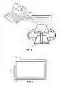
FIG. 1 is a diagrammatic perspective illustration of a display panel adapted to receive a probe card.
FIG. 2 is a diagrammatic front elevation of the display panel shown in FIG. 1, showing the locations of probe pads for receiving probe cards.
FIG. 3 is a diagram of a pair of probe pads connected to a multiplexer used to supply probe signals to the probe pads.
FIG. 4 is a schematic circuit diagram of one of the probe pads illustrated in FIG. 3 connected to receive the display signals.
FIG. 5 is a diagrammatic illustration of an inspection system for taking measurements of an AMOLED panel, and various corrective actions that can be taken to fix defects identified by analysis of the measurements.
FIG. 6 is a schematic circuit diagram of a pixel circuit having a signal WR.
While the invention is susceptible to various modifications and alternative forms, specific embodiments have been shown by way of example in the drawings and will be described in detail herein. It should be understood, however, that the invention is not intended to be limited to the particular forms disclosed. Rather, the invention is to cover all modifications, equivalents, and alternatives falling within the spirit and scope of the invention as defined by the appended claims.
DETAILED DESCRIPTION
FIG. 1 illustrates a system for inspecting an OLED display panel 10 at one or more stages of the fabrication of the panel 10 (e.g., a TFT backplane, a fully fabricated panel, or a fully completed and sealed panel). The display panel 10 is coupled to a computer 14 through measurement electronics 11 and a probe card 12, to provide the capability of testing and verifying the panel at each processing step. For example, after finishing the TFT backplane, the probe card system can be used to measure the performance of the TFT backplane by itself. If the TFT backplane is acceptable, then the panel 10 is passed to the next step which can be the OLED deposition stage. After the OLED deposition is completed, the panel 10 can be measured for proper OLED deposition before sealing. After sealing, the panel 10 can be measured again before it is sent to an assembly process.
As can be seen in FIG. 2, the illustrative display panel 10 has probe pads 20 formed along three of the four edges of the panel. Probe pads can also be formed inside the panel, preferably before the OLED deposition stage. The probe pads 20 are used to supply test signals to the numerous pixel circuits on the display panel 10, via bonding pads 30 formed at the outer ends of the various signal lines leading to the pixel circuits.
FIG. 3 illustrates the connection of the probe pads 20 to the bonding pads 30 through a multiplexer (MUX) 40, to reduce the required number of probe pads, which in turn permits the pad pitch to be increased. To ensure that the other signals connected to the probe pads 20 are biased properly, the MUX 40 needs to be capable of connecting each probe pad 20 to a common signal (Vcom) for each group of signals (e.g., source signals, gate signals, etc.).
FIG. 4 illustrates a MUX 40 with common signal control and two or more panels signals for each probe pad 20. FIG. 4 illustrates h panel signals connected to one probe pad 20, thus requiring 2 h controlling signals for connection to the probe pads 20 or connection to the common signals. The connections of the panel signals to the probe pad 20 are controlled by first switches 41 and 42, and the connections of the common signals Vcom to the panel signal lines are controlled by second switches 43 and 44.
The proper pad pitch for full panel probing is typically about 150 μm. As illustrated by the data in Table 1, the pad pitch for most conventional configurations meets the minimum pad pitch requirements. However, using multiplexing ratios of 2:1 or greater permits the pad pitch to be increased, resulting in much simpler probe cards, as also illustrated by the data in Table 1:
| TABLE 1 |
| Pad pitch for different display sizes and resolutions. |
| Gate Pad | Source Pad | EIC Pad | |||
| Pitch | Pitch | Pitch | |||
| Panel | MUX | (μm) | (μm) | (μm) | |
| 55″ HD | 1:1 | 295 | 330 | 330 | |
| 55″ HD | 2:1 | 592 | 661 | 661 | |
| 55″ HD | 8:1 | 2370 | 2645 | 2645 | |
| 55″ UD | 1:1 | 148 | 165 | 165 | |
| 55″ UD | 2:1 | 295 | 330 | 330 | |
| 55″ UD | 8:1 | 1185 | 1132 | 1132 | |
| 78″ UD | 1:1 | 222 | 222 | 222 | |
| 78″ UD | 2:1 | 444 | 445 | 445 | |
| 78″ UD | 8:1 | 1777 | 1781 | 1781 | |
As depicted in FIG. 5, an electronic measuring system 13 mounted on the probe card 12 can measure the electrical characteristics of every TFT and every OLED device in a display panel 10 and identify defects and non-uniformities. This data is supplied to a GUI 14, where the data can be used to fine-tune every process step, to achieve higher yields, faster process ramp-up, and lower line monitoring costs. Examples of the various process steps that can be fine tuned are illustrated in FIG. 5, namely, a sputtering and PECVD module 50, a process annealing module 51, a patterning module 52, a laser repair module 53, an inkjet printing module 54 and an evaporation module 55. The end result is a complete display panel 56.
The circuitry depicted in FIG. 5 takes data from the measurement electronics 13, analyzes that data, and displays it in a wide variety of reports, tables, and pictures. Some of the views are described in the following table:
| View | Description |
| TFT Absolute | View the absolute measurement replacement values |
| LUT | for each pixel on the panel. |
| TFT Filtered | View the filtered replacement values used to |
| LUT | calculate delta values. |
| TFT Base | View the factory shipment values of the panel |
| LUT | to determine how much the pixels have aged |
| (baseline). | |
| TFT Delta | View the difference between the current average |
| LUT | measured value and the baseline values (used to |
| determine compensation). | |
| TFT Histogram | View the number of times a pixel has been measured |
| LUT | since the last time the histogram was reset. This |
| lookup table is primarily used for priority scan | |
| algorithm. | |
| TFT Pixel | View either the current state of the measurement |
| State LUT | state machine or the last comparison values for |
| each pixel. | |
| TFT Region | Show the priority of each region in the priority |
| Priority | scan algorithm. |
| OLED Absolute | View the absolute measurement replacement values |
| LUT | for each pixel on the panel OLED layer. |
| OLED Filtered | View the filtered replacement values used to |
| LUT | calculate delta values. |
| OLED Base LUT | View the factory shipment values of the panel to |
| determine how much the pixels have aged (baseline). | |
| OLED Histogram | View the number of times a pixel has been measured |
| since the last time the histogram was reset. | |
| OLED Pixel | View either the current state of the measurement |
| State | state machine or the last comparison values for |
| each pixel. | |
| OLED Region | Show the priority of each region in the priority |
| Priority | scan algorithm. |
| Dead Pixels | Show which pixels were either dead at point of |
| LUT | manufacture or have since been determined to be |
| unresponsive. Note that dead pixels are not | |
| compensated. | |
| Combine Delta | The combined TFT and OLED delta values used to |
| LUT | determine the final compensation. |
| Scratch LUT | A temporary LUT View to allow users to manipulate |
| the data without making modifications to the | |
| system tables or to simply “backup” a table. | |
| Statistics | Reports the performance statistics and the current |
| frame rate. Use these statistics to compare the | |
| time required to process and display the current | |
| data in MaxLife Viewer vs. the time it would | |
| actually take if the display was not required. | |
| Pixel Trends | View the pixel state to determine if there are |
| unsettled pixels and view comparative levels. | |
| Allows you to obtain a visual representation of | |
| uncertainty zones and look at specific defective | |
| pixels. | |
| Use this option to obtain active measurements | |
| over time; determine how many times a pixel was | |
| measured before it settled. | |
| Uniformity | Select a LUT table, then analyze the uniformity. |
| Report | |
| Offset | |
| Character- | Plots the V-to-I voltage DAC code to the probability |
| ization | of a comparator result flip. |
| Hardware | View the current hardware configuration parameters. |
| Configuration | |
| Display | Adds the Display Controls to the bottom of the |
| Controls | current tab. |
| These options allow you to set the frame refresh | |
| rate in frames per second. | |
| Drag the slider to the left or right to speed up or | |
| slow down the refresh rate. Slower speeds are more | |
| visible to the naked eye. | |
| CLI View | Issues commands from MaxLife Viewer to the system. |
A wide variety of different circuitry and algorithms may be used for extracting measurements of different parameters from the display panel at different stages of its fabrication, such as the extraction systems described in U.S. patent application Ser. No. 13/835,124 filed Mar. 15, 2013 and entitled “Systems and Methods for Extrraction of Threshold and Mobility Parameters in AMOLED Displays,” which is incorporated by reference herein in its entirety.
The inspection system can identify many potential defects and problems (e.g., with sputtering and PECVD steps, that can be used to identify the likely cause of the defect or problem so that the fabricating process can be immediately fine-tuned to correct the problem). Examples of such issues and their likely causes are the following:
| Issue identified by MaxLife ™ | |
| inspection system | Likely cause |
| Line defect (open circuit | Particle defect during deposition, |
| on metal lines) | poor adhesion, contaminated substrate |
| and poor step coverage. | |
| High resistance or non- | Non-uniform sputtering process, |
| uniform resistance on metal | contaminated sputter gas or process |
| lines | chamber. |
| Non-uniform TFT contact | Problem with n+ layer PECVD step, |
| resistance | incomplete via etch or photoresist |
| stripping process. | |
| Vt or mobility of TFTs out | Problem with a-Si layer PECVD step |
| of specification | (contamination during deposition, |
| process parameter drift or film stress) | |
| Open TFT channel | Problem with a-Si or n+ layer deposi- |
| tion (particle contamination during | |
| deposition/contaminated substrate) | |
| Gate shorted to fixed | Incomplete metal patterning and/or |
| voltage | damaged dielectric layers from |
| particles or ESD | |
| Source or gate shorted to | Damaged dielectric layers (pinholes) |
| drain | from particles or ESD |
| Open or high resistance | Incomplete via etching. |
| contacts | |
| Out of spec capacitance | Non-uniform dielectric layer deposi- |
| tion or drift in deposition process | |
| parameters. | |
| Line defect (crossover | Pinhole in the dielectric layers from |
| short) | particles or ESD |
For defects that cannot be directly identified by a single measurement of the inspection system, the first measurement can reveal that a problem exists, and specify additional tests that will conclusively identify the exact defect. One example is the identification of line defects, which can be detected by any of the following procedures:
-
- 1. Measuring the current of different lines: if the current is higher than a threshold, the pixel is shorted.
- 2. Applying pulse to measure the charge transfer: if the amount of charge transfer is smaller than a threshold, the line is open.
- 3. For a signal with connection to DC current (e.g., Vdd and Vmonitor), the current can be measured to detect the open defect
Defects in the thin film transistors (TFTs) can also be detected. For example, in the situation where the pixel circuit in FIG. 6 has a signal WR measured as high (while Vdata=high, and also while Vdata=low, and Vdd=high), an additional test needs to be performed. Table 1 shows the different conditions and what the results mean.
To detect problems with process annealing, the exact Vt and mobility of each TFT can be used to adjust process annealing parameters, as follows:
| Issue identified by MaxLife ™ | ||
| inspection system | Likely cause | |
| Vt and/or mobility of TFTs is higher | Laser power drift | |
| or lower than specification | ||
| Small scale non-uniformity of Vt | Intermittent laser power | |
| and/or mobility of TFTs | output | |
| Large scale non-uniformity of Vt | Laser repeatability | |
| and/or mobility of TFTs | ||
The number and types of defects can be used to identify problems in patterning (particles, under/over exposure, etc.), as follows:
| Issue identified by MaxLife ™ | |
| inspection system | Likely cause |
| High-resistance metal lines | Pattern definition or metal etch |
| process. Poor line width control. | |
| Open or high resistance | Poor via pattern definition/photo- |
| contacts | resist residue |
| Gate shorted to fixed | Pinholes in the dielectric layers. |
| voltage | |
| Abnormal capacitance or | Mask alignment error (rotation), |
| resistance in corners of | photoresist thickness non-unifor- |
| panel | mity. |
| Large scale capacitance or | Pattern alignment error or exposure |
| resistance, non-uniformity | power fluctuation. |
| Adjacent metal lines shorted | Particles in photoresist/pattern |
| definition. | |
| Pattern stitching defects | Stepper alignment failure |
| Repetitive defect | Exposure masks damage or contami- |
| nated. | |
The defect location and defect type can be used to pinpoint areas suitable for laser repair (removing material) or ion beam deposition (adding material), as follows:
| Issue identified by MaxLife ™ | |
| inspection system | Repair Step |
| Gate shorted to fixed | Give exact pixel location to laser |
| voltage | repair system |
| Short on metal lines | Identify the metal lines that are |
| shorted. | |
| Open circuit on metal lines | Identify the metal lines that are |
| open. | |
| Open or high resistance | Quickly identify the number and |
| TFT contacts | location of the defective pixels. |
The uniformity data can also be used to continuously calibrate each print head used for inkjet printing, in real-time. The system knows which print head was used to print each pixel, and thus problems with individual print heads can be detected. The print head used to print those pixels can then be immediately adjusted, as follows.
| Issue identified by MaxLife ™ | |
| inspection system | Likely cause |
| Dead pixels | Printhead occasionally putting down |
| too little material, causing shorts | |
| Stuck-on pixel | Printhead occasionally putting down |
| too little material | |
| High-resistance pixels | The printhead printing those pixels |
| may be putting down too much material | |
| Uniformity of OLED's | Flow control of printhead malfunc- |
| voltage is poor | tioning |
The exact failure mode of every OLED device can be used to tune the evaporation process, as follows:
| Issue identified by MaxLife ™ | |
| inspection system | Likely cause |
| All pixels from one printhead | Problem with calibration of |
| are too high (or too low) | printhead |
| resistance | |
| Short-circuit OLED | Too little organic material being |
| deposited, causing shorts | |
| High-resistance pixels | Too much organic material being |
| deposited | |
| OLED voltage too high | Too much organic material being |
| deposited | |
| Long-range Uniformity of | Problem with substrate rotation or |
| OLED's voltage is poor | evaporator too close to substrate |
| Short-range uniformity of | Problem with thermal evaporation |
| OLED's voltage is poor | temperature control |
| Open-circuit OLED | Particles during evaporation |
| Short to cathode or anode | Particles during evaporation |
| Partial short (low resistance) | Too little organic material being |
| deposited | |
The electrical characteristics (collected during TFT and OLED inspection) can be loaded into a lookup table, and used to correct for all TFT and OLED non-uniformities.
Additional defects can be identified once both the OLEDs and TFTs have been deposited. The first measurement can identify that a problem exists, and specify additional tests that will conclusively identify the exact defect.
If test samples are created around the periphery of the panel, then more details about the global process parameters can be extracted. Typically this is done by cutting off the test samples from a small percentage of displays and putting them in a separate characterization system. However, with the present inspection system, this can be done as part of panel characterization, for every panel, as follows:
-
- Metal lines can be created and resistance measured. This can test both metal deposition steps and etching.
- Semiconductor layers to be annealed can have their characteristics and uniformity tested.
- Structures can be used at different locations around the panel to test alignment.
- OLED structures can be used to test evaporation and inkjet printing steps.
While particular embodiments and applications of the present invention have been illustrated and described, it is to be understood that the invention is not limited to the precise construction and compositions disclosed herein and that various modifications, changes, and variations can be apparent from the foregoing descriptions without departing from the spirit and scope of the invention as defined in the appended claims.
Claims
1. A method of inspecting at least a portion of a display panel having pixel circuits that include thin film transistors (TFTs) and organic light emitting devices (OLEDs), during or immediately following fabrication, so that adjustments can be made to the fabrication procedures to avoid defects and non-uniformities in said pixel circuits, said method comprising
providing bonding pads connected to signal lines on at least portions of the display panel,
providing probe pads along selected edges of said portions of the display panel, and
coupling said probe pads to said bonding pads through a plurality of multiplexers so that the number of probe pads can be smaller than the number of bonding pads.
2. The method of claim 1 which includes measurement electronics coupled to said probe pads, and a computer coupled to said measurement electronics.
3. The method of claim 1 in which said probe pads are formed along a plurality of edges of said display panel.
4. The method of claim 1 which includes supplying test signals to the pixel circuits on the display panel via said probe pads.
5. The method of claim 1 in which said display panel is an AMOLED display panel.
6. The method of claim 1 in which each of said multiplexers is capable of connecting each probe pad to common signals (Vcom) for multiple groups of signals.
7. The method of claim 1 which each multiplexer includes first switches providing connections of multiple panel signal lines to a probe pad, and second multiplexers providing connections of common signals to panel signal lines.
8. The method of claim 1 which includes measuring the electrical characteristics of every TFT and every OLED device in the display panel, and identifying defects and non-uniformities in the panel based on the measured electrical characteristics.
9. A display panel having a multiplicity of pixel circuits that include thin film transistors and organic light emitting devices OLEDs), said display panel comprising
multiple signal lines on portions of the display panel,
multiple bonding pads connected to said signal lines,
multiple probe pads positioned along selected edges of the portions of the display panel that have said signal lines, and
multiple multiplexers coupling said probe pads to said bonding pads.
10. The display panel of claim 9 which includes measurement electronics coupled to said probe pads, and a computer coupled to said measurement electronics.
11. The display panel of claim 9 in which said probe pads are formed along a plurality of edges of said display panel.
12. The display panel of claim 9 which said probe pads supply test signals to the pixel circuits on the display panel.
13. The display panel of claim 9 in which said display panel is an AMOLED display panel.
14. The display panel of claim 9 in which each of said multiplexers is capable of connecting each probe pad to common signals (Vcom) for multiple groups of signals.
15. The display panel of claim 9 which each multiplexer includes first switches providing connections of multiple panel signal lines to a probe pad, and second multiplexers providing connections of common signals to panel signal lines.
16. The display panel of claim 9 which includes a processor configured to measure the electrical characteristics of every TFT and every OLED device in the display panel, and to identify defects and non-uniformities in the panel based on the measured electrical characteristics.
Images & Drawings included:


Sources:
- United States Patent and Trademark Office - verify current appl. status at the USPTO↗
Recent applications in this class:
- » 20250292711 2025-09-18
DISPLAY APPARATUS AND METHOD OF DRIVING DISPLAY PANEL USING THE SAME - » 20250285570 2025-09-11
DRIVER CHIP, AND STATE SELF-TEST METHOD THEREFOR - » 20250285569 2025-09-11
LIGHT-EMITTING SUBSTRATE AND DISPLAY APPARATUS - » 20250285568 2025-09-11
METHOD OF TESTING COMPENSATION OPERATION AND COMPENSATION OPERATION TEST SYSTEM PERFORMING THE SAME - » 20250285567 2025-09-11
DISPLAY DEVICE AND METHOD OF DRIVING DISPLAY DEVICE - » 20250279020 2025-09-04
Display Device - » 20250279019 2025-09-04
DISPLAY SYSTEM AND METHOD OF OPERATING DISPLAY SYSTEM - » 20250279018 2025-09-04
FLEXIBLE VOLTAGE GATE HIGH (VGH) SETTING AND VOLTAGE CALIBRATION - » 20250273106 2025-08-28
ELECTRONIC PANEL AND ELECTRONIC APPARATUS INCLUDING THE SAME - » 20250273105 2025-08-28
APPARATUS AND METHOD FOR DETERMINING STATUS OF FLEXIBLE DISPLAY
Recent applications for this Assignee:
- » 20210407393 2021-12-30
Display system using system level resources to calculate compensation parameters for a display module in a portable device - » 20210312863 2021-10-07
AMOLED displays with multiple readout circuits - » 20210312862 2021-10-07
Pixel circuits for AMOLED displays - » 20210280129 2021-09-09
Systems and methods of pixel calibration based on improved reference values - » 20210272516 2021-09-02
Display panel compensation methods - » 20210256915 2021-08-19
System and methods for aging compensation in AMOLED displays - » 20210250574 2021-08-12
Optical correction systems and methods for correcting non-uniformity of emissive display devices - » 20210217832 2021-07-15
Pixel having an organic light emitting diode and method of fabricating the pixel - » 20210210024 2021-07-08
Pixel measurement through data line - » 20210097935 2021-04-01
Cleaning common unwanted signals from pixel measurements in emissive displays