LED array
US20140319574A1
2014-10-30
14/330,914
2014-07-14
✅ Patent granted
US 9,202,981 B2
2015-12-01
-
-
Dung Le
Ditthavong & Steiner, P.C.
2034-07-14
Abstract:
An LED array having N light-emitting diode units (N≧3) comprises a permanent substrate, a bonding layer on the permanent substrate, a second conductive layer on the bonding layer, a second isolation layer on the second conductive layer, a crossover metal layer on the second isolation layer, a first isolation layer on the crossover metal layer, a conductive connecting layer on the first isolation layer, an epitaxial structure on the conductive connecting layer, and a first electrode layer on the epitaxial structure. The light-emitting diode units are electrically connected with each other by the crossover metal layer.
Inventors:
- Li-Ping JOU 6 🇹🇼 Kaohsiung City, Taiwan
- Yu-Chen YANG 7 🇹🇼 Tainan City, Taiwan
- Jui-Hung YEH 6 🇹🇼 Zhongli City, Taiwan
- Li-Ping Jou 6 🇹🇼 Kaohsiung, Taiwan
- Yu-Chen Yang 6 🇹🇼 Tainan, Taiwan
- Jui-Hung Yeh 6 🇹🇼 Zhongli, Taiwan
Assignee:
- EPISTAR CORPORATION 1,112 🇹🇼 Hsinchu, Taiwan
Applicant:
Interested in similar patents?
Get notified when new applications in this technology area are published.
Classification:
H01L27/15 IPC
Devices consisting of a plurality of semiconductor or other solid-state components formed in or on a common substrate including semiconductor components with at least one potential-jump barrier or surface barrier specially adapted for light emission
H01L27/153 » CPC further
Devices consisting of a plurality of semiconductor or other solid-state components formed in or on a common substrate including semiconductor components with at least one potential-jump barrier or surface barrier specially adapted for light emission in a repetitive configuration, e.g. LED bars
H01L33/36 » CPC main
Semiconductor devices with at least one potential-jump barrier or surface barrier specially adapted for light emission; Processes or apparatus specially adapted for the manufacture or treatment thereof or of parts thereof; Details thereof characterised by the electrodes
H01L27/156 » CPC further
Devices consisting of a plurality of semiconductor or other solid-state components formed in or on a common substrate including semiconductor components with at least one potential-jump barrier or surface barrier specially adapted for light emission in a repetitive configuration, e.g. LED bars two-dimensional arrays
H01L33/08 » CPC further
Semiconductor devices with at least one potential-jump barrier or surface barrier specially adapted for light emission; Processes or apparatus specially adapted for the manufacture or treatment thereof or of parts thereof; Details thereof characterised by the semiconductor bodies with a plurality of light emitting regions, e.g. laterally discontinuous light emitting layer or photoluminescent region integrated within the semiconductor body
H01L33/382 » CPC further
Semiconductor devices with at least one potential-jump barrier or surface barrier specially adapted for light emission; Processes or apparatus specially adapted for the manufacture or treatment thereof or of parts thereof; Details thereof characterised by the electrodes with a particular shape the electrode extending partially in or entirely through the semiconductor body
H01L2933/0016 » CPC further
Details relating to devices covered by the group but not provided for in its subgroups; Processes relating to electrodes
H01L21/00 IPC
Processes or apparatus adapted for the manufacture or treatment of semiconductor or solid state devices or of parts thereof
H01L33/38 IPC
Semiconductor devices with at least one potential-jump barrier or surface barrier specially adapted for light emission; Processes or apparatus specially adapted for the manufacture or treatment thereof or of parts thereof; Details thereof characterised by the electrodes with a particular shape
Description
REFERENCE TO RELATED APPLICATION
This application is a Divisional Application of U.S. patent application Ser. No. 14/065,330, entitled “LED ARRAY”, filed Oct. 28, 2013, now pending, which is a division of U.S. patent application Ser. No. 13/428,974, entitled “LED ARRAY”, filed on Mar. 23, 2012, now pending, which claims the right of priority based on Taiwan patent application Ser. No. 100110029, filed Mar. 23, 2011, the entireties of which are incorporated by reference herein.
TECHNICAL FIELD
The application relates to an LED array, and more particularly to an LED array having N light-emitting diode units (N≧3).
DESCRIPTION OF BACKGROUND ART
Recently, based on the progress of epitaxy process technology, the light-emitting diode (LED) becomes one of the potential solid-state lighting (SSL) source. Due to the limitation of physics mechanism, LEDs can only be driven by DC power source. Thus the regulator circuit, buck circuit, and other electronic devices are necessary for every lighting device using LED as lighting source to convert AC power source into DC power source to drive LED. However, the addition of the regulator circuit, buck circuit, and other electronic device raises the cost of lighting device using LED as lighting source and causes the low AC/DC conversion efficiency and the huge lighting device package also affect the reliability and shorten the lifetime of LED in daily use.
SUMMARY OF THE DISCLOSURE
The present application discloses an LED array comprising a permanent substrate, a bonding layer on the permanent substrate, a second conductive layer on the bonding layer, a second isolation layer on the second conductive layer, a crossover metal layer on the second isolation layer, a first isolation layer on the crossover metal layer, a conductive connecting layer on the first isolation layer, an epitaxial structure on the conductive connecting layer, and a first electrode layer on the epitaxial structure.
The present application further discloses an LED array comprising a permanent substrate, a bonding layer on the permanent substrate, a first conductive layer on the bonding layer, a second isolation layer on the first conductive layer, a crossover metal layer on the second isolation layer, a first isolation layer on the crossover metal layer, a conductive connecting layer on the first isolation layer, and an epitaxial structure on the conductive connecting layer.
The present application further discloses an Led array having N light-emitting diode units (N≧3) and the light-emitting diode units are electrically connected with each other by the crossover metal layer.
BRIEF DESCRIPTION OF THE DRAWINGS
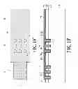
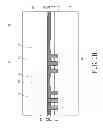
FIGS. 1A-1I are the cross sectional views of the LED array in accordance of the first embodiment of present application.
FIGS. 1A′-1G′ are the top views of the first embodiment of LED array disclosed by present application.
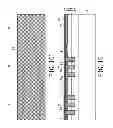
FIGS. 2A-2I are the cross sectional views of the second embodiment of LED array disclosed by present application.
FIGS. 2A′-2G′ are the top views of the second embodiment of LED array disclosed by present application.
DETAILED DESCRIPTION OF PREFERRED EMBODIMENTS
The present application discloses an LED array having N light-emitting diode units (N≧3) comprising a first light-emitting diode unit, a second light-emitting diode unit in sequence to the (N−1)th light-emitting diode unit and an Nth light-emitting diode unit. The LED array further comprises a first area (I), the second area (II), and the third area (III). The first area (I) comprises the first light-emitting diode unit, the third area (III) comprises the Nth light-emitting diode unit, and the second area (II) locates between the first area (I) and the third area (III) and comprises the second light-emitting diode unit in sequence to the (N−1)th diode units.
The first embodiment discloses a first LED array 1 having three light-emitting diode units. FIGS. 1A to 1I illustrate the cross sectional views and the FIGS. 1A′ to 1G′ illustrate the top views of the first embodiment of the first LED array 1. The method for manufacturing the first LED array 1 comprises steps of:
-
- 1. Providing a temporary substrate 11, and forming an epitaxial structure thereon. The epitaxial structure comprises a first conductive semiconductor layer 12, an active layer 13, and a second conductive semiconductor layer 14 as illustrated in FIGS. 1A and 1A′.
- 2. Next, forming multiple trenches 15 by partially etching the epitaxial structure in the first area (I) and the second area (II), and the epitaxial structure not etched forms multiple flat planes 16, and the epitaxial structure of the third area (III) is not etched as illustrated in FIGS. 1B and 1B′.
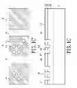
- 3. Forming a conductive connecting layer 17 on partial regions of the flat planes 16, and the area of the flat planes 16 uncovered by the conductive connecting layer 17 forms multiple pathways 18 as illustrated in FIGS. 1C and 1C′.
- 4. Forming a first isolation layer 19 on part of the conductive connecting layer 17, the multiple pathways 18, and the side wall of the multiple trenches 15, while the conductive connecting layer 17 in the third area (III) and part of the conductive connecting layer 17 in the first area (I) are not covered by the first isolation layer 19. The conductive connecting layer 17 not covered by the first isolation layer 19 in the second area (II) is defined as a conductive region 20 as illustrated in FIGS. 1D and 1D′.
- 5. Forming a crossover metal layer 21 on the first isolation layer 19, the conductive region 20, in multiple trenches 15, and on the conductive connecting layer 17 in the third area (III). A part of the conductive connecting layer 17 in the first area (I) is not covered by the crossover metal layer 21 in order to electrically connect the second conductive layer 23 with the second conductive semiconductor layer 14 in the following steps. The region which is not covered by the crossover metal layer 21 in the second area (II) nearby the conductive region 20 is used for electrical isolation as illustrated in the FIGS. 1E and 1E′. Part of the crossover metal layer 21 in the first area (I) extends to multiple trenches 15 and electrically connects to the first conductive semiconductor layer 12. The crossover metal layer 21 on multiple flat planes 16 and the pathways 18 in the first area (I) is electrically isolated from the second conductive semiconductor layer 14 by the first isolation layer 19. The crossover metal layer 21 on the conductive region 20 in the second area (II) electrically connects with the second conductive semiconductor layer 14 by the conductive connecting layer 17. Part of the crossover metal layer 21 in the second area (II) extends to multiple trenches 15 and electrically connects to the first conductive semiconductor layer 12. The crossover metal layer 21 on multiple flat planes 16 and the pathways 18 in the second area (II) is electrically isolated from the second conductive semiconductor layer 14 by the first isolation layer 19. The crossover metal layer 21 in the third area (III) is electrically connected with the second conductive semiconductor layer 14 by the conductive connecting layer 17.
- 6. Forming a second isolation layer 22 on the crossover metal layer 21 and the region a in the second area (II). But part of the conductive connecting layer 17 in the first area (I) is not covered by the second isolation layer 22 as illustrated in the FIGS. 1F and 1F′.
- 7. Forming the second conductive layer 23 on the second isolation layer 22 and part of the conductive connecting layer 17 as illustrated in the as illustrated in the FIGS. 1G and 1G′.
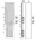
- 8. Forming a bonding layer 24 on the second conductive layer 23 which is bonded with a permanent substrate 25 by the bonding layer 24 as illustrated in the FIG. 1H.
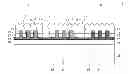
- 9. Removing the temporary substrate 11 to expose the first conductive semiconductor layer 12 and roughening the surface of the first conductive semiconductor layer 12. Next, etching multiple pathways 18 from the first conductive semiconductor layer 12 until the first isolation layer 19 is revealed in order to form N light-emitting diode units. Among the N light-emitting diode units, the first light-emitting diode unit locates in the first area (I), the second to the (N−1)th light-emitting diode units locate in the second area (II), and the Nth light-emitting diode unit locates in the third area (III). At last, forming a first electrode layer 27 on the roughed surface of the first conductive semiconductor layer 12 in the Nth light-emitting diode unit. Thus an LED array 1 having N light-emitting diode units electrically connected in serial by the crossover metal layer 21 is formed as illustrated in FIG. 1I.
The second embodiment discloses a second LED array 2 having three light-emitting diode units. FIGS. 2A to 2I illustrate the cross sectional views and the FIGS. 2A′ to 2G′ illustrate the top views of the second embodiment of LED array 2. The method for manufacturing the second LED array 2 comprises steps of:
-
- 1. Providing a temporary substrate 11, and forming an epitaxial structure thereon. The epitaxial structure comprises a first conductive semiconductor layer 12, an active layer 13, and a second conductive semiconductor layer 14 as illustrated in FIGS. 2A and 2A′.
- 2. Next, forming multiple trenches 15 by partially etching the epitaxial structure in the first area (I), the second area (II), and the third area (III), and the epitaxial structure not etched forms multiple flat planes 16 as illustrated in FIGS. 2B and 2B′.
- 3. Forming a conductive connecting layer 17 on partial regions of the flat planes 16, and the area of the flat planes 16 uncovered by the conductive connecting layer 17 forms multiple pathways 18 as illustrated in FIGS. 2C and 2C′.
- 4. Forming a first isolation layer 19 on part of the conductive connecting layer 17, the multiple pathways 18, and the side wall of the multiple trenches 15. The conductive connecting layer 17 in the second area (II) and the third area (III) which is not covered by the first isolation layer 19 are defined as a conductive region 20 as illustrated in FIGS. 2D and 2D′.
- 5. Forming a crossover metal layer 21 on the first isolation layer 19, the conductive region 20, and in the multiple trenches 15 except those in the third area (III). A part of the first isolation layer 19 in the first area (I) is not covered by the crossover metal layer 21 in order to electrically isolate the first conductive layer 26 from the second conductive semiconductor layer 14 in the following steps. The first isolation layer 19 in multiple trenches 15 and flat planes 16 is not covered by the crossover metal layer 21 in order to electrically isolate the first conductive layer 26 from the second conductive semiconductor layer 14 in the following steps as illustrated in the FIGS. 2E and 2E′. A part of the crossover metal layer 21 in the first area (I) extends to multiple trenches 15 and electrically connects to the first conductive semiconductor layer 12. The crossover metal layer 21 on multiple flat planes 16 and the pathways 18 in the first area (I) is electrically isolated from the second conductive semiconductor layer 14 by the first isolation layer 19. The crossover metal layer 21 on the conductive region 20 in the second area (II) electrically connects with the second conductive semiconductor layer 14 by the conductive connecting layer 17. A part of the crossover metal layer 21 in the second area (II) extends into the multiple trenches 15 and electrically connects to the first conductive semiconductor layer 12. The crossover metal layer 21 on multiple flat planes 16 and the pathways 18 in the second area (II) is electrically isolated from the second conductive semiconductor layer 14 by the first isolation layer 19. The crossover metal layer 21 on the conductive region 20 in the third area (III) electrically connects with the second conductive semiconductor layer 14 by the conductive connecting layer 17. Besides, the region b in the second area (II) and the third area (III) adjacent to the conductive region 20 is not fully covered by the crossover metal layer 21 which is used for electrical isolation.
- 6. Forming a second isolation layer 22 on the crossover metal layer 21, the part of the first isolation layer 19 in the first area (I), and on the region b which is not fully covered by the crossover metal layer 21 in the second area (II). The second isolation layer 22 does not cover the inner side of the trenches 15 in the third area (III), the first isolation layer 19 of the multiple flat planes 16, and the region b which is not fully covered by the crossover metal layer 21 in the third area (III) as illustrated in the FIGS. 2F and 2F′.
- 7. Forming the first conductive layer 26 on the second isolation layer 22, in the multiple trenches 15 in the third area (III), on the first isolation layer 19 of the flat planes 16, and the region b which is not fully covered by the crossover metal layer 21 in the third area (III) as illustrated in the FIGS. 2G and 2G′.
- 8. Forming a bonding layer 24 on the first conductive layer 26 which is bonded with a permanent substrate 25 by the bonding layer 24 as illustrated in the FIG. 2H.
- 9. Removing the temporary substrate 11 to expose the first conductive semiconductor layer 12 and roughs the surface of the first conductive semiconductor layer 12. Next, etching multiple pathways 18 form the first conductive semiconductor layer 12 until the first isolation layer 19 is revealed in order to form N light-emitting diode units. Among the N light-emitting diode units, the first light-emitting diode unit locates in the first area (I), the second to the (N−1)th light-emitting diode units locate in the second area (II), and the Nth light-emitting diode unit locates in the third area (III). Next, etching the first conductive semiconductor layer 12 in the first area (I) without the crossover metal layer 21 until the conductive connecting layer 17 is revealed, and forming a second electrode layer 28 on the conductive connecting layer 17. Thus an LED array 2 having N light-emitting diode units electrically connected in series by the crossover metal layer 21 is formed as illustrated in FIG. 2I.
The temporary substrate 11 described in the above first and second embodiments is made of, for example, gallium arsenide (GaAs), gallium phosphide (GaP), sapphire, silicon carbide (SiC), gallium nitride (GaN), or aluminum nitride. The epitaxial structure is made of an III-V group semiconductor material which is the series of aluminum gallium indium phosphide (AlGaInP) or the series of aluminum gallium indium nitride (AlGaInN). The conductive connecting layer 17 comprises indium tin oxide, cadmium tin oxide, antimony tin oxide, indium zinc oxide, aluminum zinc oxide, and zinc tin oxide. The first isolation layer 19 and the second isolation layer 22 can be made of an insulating material comprises silicon dioxide, titanium monoxide, titanium dioxide, trititanium pentoxide, titanium sesquioxide, cerium dioxide, zinc sulfide, and alumina. The first conductive layer 26 and the second conductive layer 23 can be made of silver or aluminum. The bonding layer 24 is an electrically conductive material made of metal or its alloys such as AuSn, PbSn, AuGe, AuBe, AuSi, Sn, In, Au, or PdIn. The permanent substrate 25 is a conductive material such as carbides, metals, metal alloys, metal oxides, metal composites, etc. The crossover metal layer 21 comprises metal, metal alloys, and metal oxides.
Although the present application has been explained above, it is not the limitation of the range, the sequence in practice, the material in practice, or the method in practice. Any modification or decoration for present application is not detached from the spirit and the range of such.
Claims
What is claimed is:1. A light-emitting diode structure comprising:
a first epitaxial unit;
a second epitaxial unit separated from the first epitaxial unit; and
a crossover metal layer comprising a first protruding portion entering the first epitaxial unit, and a flat portion connected to the second epitaxial unit and having a width substantially equal to that of the second epitaxial unit.
2. The light-emitting diode structure of claim 1, further comprising a conductive connecting layer surrounding the first protruding portion.
3. The light-emitting diode structure of claim 2, further comprising a first isolation layer arranged between the conductive connecting layer and the first protruding portion.
4. The light-emitting diode structure of claim 1, further comprising a second isolation layer having a width substantially equal to that of the light emitting diode.
5. The light-emitting diode structure of claim 1, further comprising an electrode connected to the second epitaxial unit on a side opposite to the flay portion.
6. The light-emitting diode structure of claim 1, wherein the crossover metal layer further comprises a connecting portion connecting the first protruding portion with the flat portion.
7. The light-emitting diode structure of claim 1, wherein the crossover metal layer further comprises a second protruding portion entering the first epitaxial unit and separated from the first protruding portion.
8. A light-emitting diode structure comprising:
a first epitaxial unit;
a second epitaxial unit separated from the first epitaxial unit;
a crossover metal layer comprising a first protruding portion entering the first epitaxial unit; and
a conductive layer separated from the crossover metal layer and comprising a second protruding portion entering the second epitaxial unit.
9. The light-emitting diode structure of claim 8, further comprising a conductive connecting layer surrounding the first protruding portion.
10. The light-emitting diode structure of claim 9, further comprising an electrode arranged on the conductive connecting layer.
11. The light-emitting diode structure of claim 9, wherein the conductive connecting layer has a portion not covered by the first epitaxial unit.
12. The light-emitting diode structure of claim 8, further comprising an isolation layer formed between the crossover metal layer and the conductive layer.
13. The light-emitting diode structure of claim 8, wherein the conductive layer is wider than the crossover metal layer.
14. The light-emitting diode structure of claim 8, wherein the first protruding portion has an elevation substantially equal to that of the second protruding portion.
15. The light-emitting diode structure of claim 8, wherein the conductive layer
comprises a portion arranged under the crossover metal layer.
Images & Drawings included:


Sources:
- United States Patent and Trademark Office - verify current appl. status at the USPTO↗
Similar patent applications:
- » 20230094866
PHOTOSENSITIVE TRANSFER MATERIAL FOR LED ARRAY, LIGHT SHIELDING MATERIAL FOR LED ARRAY, LED ARRAY, AND ELECTRONIC APPARATUS - » 20090315965
LED ARRAY MANUFACTURING METHOD, LED ARRAY AND LED PRINTER - » 20220415863
Fabrication of LED arrays and LED array light engines - » 20090141490
Method for diminishing dark gap in arrayed led module, arrayed LED module, and imaging apparatus thereof - » 20120295376
METHOD FOR MANUFACTURING A LED ARRAY DEVICE, AND LED ARRAY DEVICE MANUFACTURED THEREBY - » 20110063837
LED ARRAY MODULE AND LED ARRAY MODULE FRAME - » 20200211879
Layout structure between substrate, micro-LED array and micro-vacuum module for micro-LED array transfer using micro-vacuum module, and method for manufacturing micro-LED display using the same - » 20180080644
Heatsink including thick film layer for UV LED arrays, and methods of forming UV LED arrays - » 20220293673
LED array and method of forming a LED array - » 20150219326
Modular LED array grid and method for providing such modular LED array grid
Recent applications in this class:
- » 20240387777 2024-11-21
DISPLAY PANELS AND DISPLAY DEVICES - » 20240332456 2024-10-03
LIGHTING DEVICE HAVING HIGH LUMINOUS-EFFICIENCY LAYOUT STRUCTURE - » 20240250214 2024-07-25
GALLIUM NITRIDE-BASED SEMICONDUCTOR DEVICE ON AMORPHOUS SUBSTRATE - » 20240243228 2024-07-18
DISPLAY DEVICE AND METHOD OF MANUFACTURING THE SAME - » 20240113260 2024-04-04
DISPLAY DEVICE AND MANUFACTURING METHOD OF THE SAME - » 20240006557 2024-01-04
LED CIRCUIT BOARD STRUCTURE, LED TESTING AND PACKAGING METHOD AND LED PIXEL PACKAGE - » 20220254958 2022-08-11
Display device and method of manufacturing the same - » 20210305456 2021-09-30
Semiconductor light-emitting device and semiconductor light-emitting component - » 20210217928 2021-07-15
Light emitting device, method for making the same and display apparatus - » 20210119084 2021-04-22
Optoelectronic device with transparent insulated current blocking region and uniform current spreading
Recent applications for this Assignee:
- » 20240313146 2024-09-19
LIGHT-EMITTING MODULE AND DISPLAY APPARATUS - » 20240258455 2024-08-01
METHOD OF PROCESSING LIGHT-EMITTING ELEMENTS, SYSTEM AND DEVICE USING THE SAME - » 20240234660 2024-07-11
Light-emitting device and manufacturing method thereof - » 20240234635 2024-07-11
SEMICONDUCTOR LIGHT-EMITTING DEVICE - » 20240194724 2024-06-13
Light-emitting device - » 20240186449 2024-06-06
SEMICONDUCTOR DEVICE, SEMICONDUCTOR COMPONENT AND DISPLAY PANEL INCLUDING THE SAME - » 20240186446 2024-06-06
METHOD OF SELECTIVELY TRANSFERRING SEMICONDUCTOR DEVICE - » 20240167640 2024-05-23
Lighting apparatus - » 20240162380 2024-05-16
Semiconductor device - » 20240154065 2024-05-09
Optoelectronic device and method for manufacturing the same