Optical air slit and method for manufacturing optical air slits
US20140335458A1
2014-11-13
14/444,294
2014-07-28
✅ Patent granted
US 9,235,115 B2
2016-01-12
-
-
Roberts Culbert
Daly, Crowley, Mofford & Durkee, LLP
2034-07-28
Abstract:
A structure having an optical slit therein. The structure includes a substrate having an opening therethrough and a metal layer disposed on the substrate, such metal layer having a photolithographically formed slit therein, such slit being narrower than the opening and being disposed over the opening, portions of the metal layer disposed adjacent the slit being suspended over the opening and other portions of the metal layer being supported by the substrate.
Assignee:
- RAYTHEON COMPANY 5,596 🇺🇸 Waltham, MA, United States
Applicant:
Interested in similar patents?
Get notified when new applications in this technology area are published.
Classification:
G03F7/0035 » CPC main
Photomechanical, e.g. photolithographic, production of textured or patterned surfaces, e.g. printing surfaces; Materials therefor, e.g. comprising photoresists; Apparatus specially adapted therefor Multiple processes, e.g. applying a further resist layer on an already in a previously step, processed pattern or textured surface
G03F7/00 IPC
Photomechanical, e.g. photolithographic, production of textured or patterned surfaces, e.g. printing surfaces; Materials therefor, e.g. comprising photoresists; Apparatus specially adapted therefor
G03F7/20 » CPC further
Photomechanical, e.g. photolithographic, production of textured or patterned surfaces, e.g. printing surfaces; Materials therefor, e.g. comprising photoresists; Apparatus specially adapted therefor Exposure; Apparatus therefor
G02B5/005 » CPC further
Optical elements other than lenses Diaphragms
Y10T428/24314 » CPC further
Stock material or miscellaneous articles; Structurally defined web or sheet [e.g., overall dimension, etc.] including aperture; Noncircular aperture [e.g., slit, diamond, rectangular, etc.] Slit or elongated
G03F7/40 » CPC further
Photomechanical, e.g. photolithographic, production of textured or patterned surfaces, e.g. printing surfaces; Materials therefor, e.g. comprising photoresists; Apparatus specially adapted therefor; Processing photosensitive materials; Apparatus therefor Treatment after imagewise removal, e.g. baking
G01J3/0229 » CPC further
Spectrometry; Spectrophotometry; Monochromators; Measuring colours; Details; Optical elements not provided otherwise, e.g. optical manifolds, diffusers, windows using masks, aperture plates, spatial light modulators or spatial filters, e.g. reflective filters
B29D11/00 IPC
Producing optical elements, e.g. lenses or prisms
G02B5/00 IPC
Optical elements other than lenses
G01J3/02 IPC
Spectrometry; Spectrophotometry; Monochromators; Measuring colours Details
Description
CROSS REFERENCE TO RELATED APPLICATION
This application is a divisional of and claims the benefit of application Ser. No. 13/278,254 filed Oct. 21, 2011.
TECHNICAL FIELD
This disclosure relates generally to optical slits and more particularly to method for making relatively long, narrow optical air slits.
BACKGROUND
As is known in the art, air slits have a wide range of use in optics. One such use is in hyper spectral imaging system where such systems are used to collect and process information from across the electromagnetic spectrum that can extend beyond the visible band.
As is also known, techniques used to faun air optical slits include the use of laser cutting, photolithography, Electro Discharge Machining (EDM), thin film deposition, e-beam lithography, RF/DC & reactive sputtering, Chemical Vapor Deposition (CVD), Physical Vapor Deposition (PVD). Chemical wet etch, electroplating, electro etching, spotter etching and ion milling.
SUMMARY
In accordance with the disclosure, a structure is provided having an optical slit therein, comprising: a substrate having an opening there through; and a metal layer disposed on the substrate, such metal layer having a slit therein, such slit being narrower than the opening and being disposed over the opening, portions of the metal layer disposed adjacent the slit being suspended over the opening and other portions of the metal layer being supported by the substrate.
In one embodiment, a method is provided for forming a structure having an optical slit therein. The method includes: forming an opening through a portion of a substrate; filling the opening with a sacrificial material, such material extending through a portion of the opening with portion of the material being disposed onto adjacent portions of an upper surface of the substrate; polishing the sacrificial material to remove the portions of the sacrificial material disposed onto adjacent portions of the upper surface of the substrate; forming a metalized layer on the upper surface of the substrate and the polished sacrificial material; applying a photolithographically processable material on an upper surface of the metalized layer; photolihographically forming a slit in the photolithographically processable material to expose a portion of the upper surface of the metallized layer, such slit being disposed over the opening in the portion of the substrate; etching to remove the exposed portion of the upper surface of the metalized layer to expose the sacrificial material while retaining unexposed portions of the metallized layer; and removing the sacrificial layer and the photolithographically processable material.
In one embodiment, the unexposed portions of the metallized layer are electroplated to a predetermined thickness.
In one embodiment, the electroplating is performed prior to the forming of the slit.
In one embodiment, the electroplating is performed subsequent to forming of the slit.
In one embodiment, the opening is formed using laser cutting.
The details of one or more embodiments of the disclosure are set forth in the accompanying drawings and the description below. Other features, objects, and advantages of the disclosure will be apparent from the description and drawings, and from the claims.
DESCRIPTION OF DRAWINGS
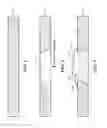
FIGS. 1-8 show a sequence of steps used to form a structure having an optical slit therein according to the disclosure.
Like reference symbols in the various drawings indicate like elements.
DETAILED DESCRIPTION
Referring now to FIGS. 1-8, steps used to form a structure having an optical slit therein are illustrated. Thus, referring to FIG. 1, a substrate 10 is provided. Here the substrate 10 is, for example, Aluminum Oxide, Silicon Nitride, Beryllium oxide or any rigid material with low coefficient of thermal expansion, here for example in the range of 0.55×10⁻⁶/° C. to 8.4×10⁻⁶/° C. Here, the substrate 10 has a thickness in the range of 3 to 10 mils.
Next, an opening 12 (FIG. 2) is formed through a portion of the substrate 10. Here, for example, the opening 12 is formed using laser cutting. The opening 12 has a span in the order 1 to 2 mils.
Next, the opening 12 is filled with a sacrificial material 14, such material having portions 14a extending through the opening 12 with portion 14b of the material 12 being disposed onto adjacent portions of an upper surface 16 of the substrate 10, as shown in FIG. 3. Here, the sacrificial matter 14 is adhesively bonded to the substrate 10 and is here, for example, Crystalbond 590, Manufactured by Electron Microscopy Sciences, P.O. Box 550, 1560 Industry Road, Hatfield, Pa. 19440, Sycast manufactured by Emerson & Cuming, Henkel Corporation, Canton (Electronic Materials) 869 Washington Street, Canton, Mass. 02021, United States Or AZ-photo resist AZ Electronics Materials (USA) corp., 70 Meister Ave. Somerville, N.J. 088764252, Next, the upper surface of the structure is polished to remove the portions 14a, 14b of the sacrificial material 14 disposed onto adjacent portions of the upper surface 16 of the substrate 10 as shown in FIG. 4.
Next, a metalized layer 18 is deposited, for example electroplated, on the upper surface of the substrate 12 and the polished sacrificial material 14, as shown in FIG. 5. Here, for example, the metalized layer 18 is formed by E-Beam, Sputtering, Electrolysis and laminating methods. The metallization layer 18 is here for example, a refractory metal such as titanium tungsten or chromium. Here the metallization layer 18 may be initially formed as a relatively thin seed layer, for example, having a thickness in the range of 150 to 250 Angstroms, or be formed with a thickness by electroplating in the range of 0.5 to 2 mils,
Next, a conventional photolithographically processable material 20 is deposited on an upper surface of the metalized layer 18, as shown in FIG. 6.
Next, a slit 24 is photolihographically formed in the photolithographically processable material 20 using any conventional photolithographic-etching technique to expose an underlying portion of the upper surface of the metallized layer 18, such slit being disposed over the filled opening 12 in FIG. 1 in the portion. of the substrate 10, as shown in FIG. 7. Here, the slit 24 has a width in the range of 5 um to 60 um and a length in the range of Tinun to 11.2 mm.
Next, the exposed underlying portion of the metalized layer 18 is removed by any conventional etching process to foam there a slit 26 having a width in the range of 5 um to 60 um and a length in the range of 77 mm to 112 mm, as shown in FIG. 7. It is noted that the slits 24, 26 expose the sacrificial material 14 while retaining unexposed portions of the metallized layer 18.
Next, the photoresist layer 20 is removed.
Next, the metalized layer 18, here acts as a seed layer and is electroplated with material 28; here material 25 is, for example, gold, copper, nickel, chromium or any standard electroplate able metal used in the electroplating business, to form the resulting metalized layer 18 with a resulting predetermined thickness, here in the range of 0.5 mil to 1 mil; it being noted that the electroplating leaves a slit 26 in the material 28 so that slits 24, 26 are formed in the resulting metalized layer 18. It should be noted that the metalized layer 18 may be formed by electroplating the unexposed portions of the metallized layer to a predetermined thickness either prior to forming the slit 26 or subsequent to forming the slit 26.
Next, the sacrificial layer 14 is removed using for example, chemical solvents, epoxy stripper, oxygen plasma, and oxygen ion milling to form the structure shown in FIG. 8. Thus, the structure shown in FIG. 8 is a structure having an optical slit 24, 26 therein, comprising: substrate 10 having the opening 12 therethrough; and a metal layer 16, 18 disposed on the substrate 10, such metal layer 16. 18 having a slit 24, 26 therein, such slit 24, 26 being narrower than the opening 12 and being disposed over the opening 12, portions of the metal layer 16a, 18a disposed adjacent the slit 24, 26 being suspended over the opening 12 and other portions of the metal layer 16, 18 being supported by the substrate 10.
A number of embodiments of the disclosure have been described. Nevertheless, it will be understood that various modifications may be made without departing from the spirit and scope of the disclosure. Accordingly, other embodiments are within the scope of the following claims.
Claims
What is claimed is:1. A method for forming a structure having an optical slit therein, comprising;
forming an opening through a portion of a substrate;
filling the opening with a sacrificial material, such material extending through a portion of the opening with portion of the material being disposed onto adjacent portions of an upper surface of the substrate;
polishing the sacrificial material to remove the portions of the sacrificial material disposed onto adjacent portions of the upper surface of the substrate;
forming a metalized layer on the upper surface of the substrate and the polished sacrificial material;
applying a photolithographically processable material on an upper surface of the metalized layer;
photolihographically forming a slit in the photolithographically processable material to expose a portion of the upper surface of the metallized layer, such slit being disposed over the opening in the portion of the substrate;
etching to remove the exposed portion of the upper surface of the metaled layer to expose the sacrificial material while retaining unexposed portions of the metallized layer;
removing the sacrificial layer and the photolithographically processable material.
2. The method recited in claim 1 including electroplating the unexposed. portions of the metallized layer to a predetermined thickness.
3. The method recited in claim 2 wherein the electroplating is performed prior to the forming of the slit.
4. The method recited in claim 2 wherein the electroplating is performed subsequent to fanning of the slit.
5. The method recited in claim 1 wherein the opening is formed using laser cutting.
Images & Drawings included:


Sources:
- United States Patent and Trademark Office - verify current appl. status at the USPTO↗
Similar patent applications:
Recent applications in this class:
- » 20250172869 2025-05-29
WAFER END PROTECTIVE-FILM FORMING COMPOSITION FOR SEMICONDUCTOR MANUFACTURING - » 20250068064 2025-02-27
ANTI-SPACER BASED SELF-ALIGNED HIGH ORDER PATTERNING - » 20250044684 2025-02-06
SYSTEMS AND METHODS FOR MANUFACTURING ELECTRONIC DEVICES - » 20240419068 2024-12-19
STRUCTURES FOR PATTERNING AND RELATED METHODS AND SYSTEMS - » 20240393683 2024-11-28
SUBSTRATE PROCESSING SYSTEM AND ARTICLE MANUFACTURING METHOD - » 20240288765 2024-08-29
FLOW CELLS AND METHODS FOR MAKING THE SAME - » 20240248395 2024-07-25
Lithographic Method for Imprinting Three-Dimensional Microstructures Having Oversized Structural Heights Into a Carrier Material - » 20240219829 2024-07-04
HYDROPHOBIC CROSSLINKABLE PINNING UNDERLAYERS WITH IMPROVED DRY ETCH CAPABILITIES FOR PATTERNING DIRECTED SELF-ASSEMBLY OF PS-B-PMMA TYPE BLOCK COPOLYMERS - » 20230418156 2023-12-28
METHOD OF MANUFACTURING A SEMICONDUCTOR DEVICE AND SEMICONDUCTOR DEVICE MANUFACTURING TOOL - » 20230400763 2023-12-14
LITHOGRAPHY SYSTEM AND METHODS
Recent applications for this Assignee:
- » 20250167415 2025-05-22
ENHANCED BROADBAND RING RESONATOR FOR IMPROVED SPECTRAL SUPPRESSION - » 20250145355 2025-05-08
INTEGRATED CABLE PACKAGING, DEPLOYMENT AND STRUMMING MITIGATION SYSTEM - » 20250118501 2025-04-10
MICRO-ELECTROMECHANICAL SYSTEMS SWITCH WITH BEAM MOVEMENT ORTHOGONAL TO FORCE - » 20250116997 2025-04-10
PRODUCT IDENTIFICATION AND TRACKING SYSTEMS AND METHODS - » 20250116851 2025-04-10
REIMAGING LENS ASSEMBLY WITH ANGLED OPTIC - » 20250107006 2025-03-27
RF COVER LAYER - » 20250067792 2025-02-27
DEVICE FOR AND METHOD OF FREQUENCY TESTING PRINTED CIRCUIT BOARD UNDER THERMAL STRESS - » 20250062543 2025-02-20
CONFORMAL WAVEFRONT TRANSFORMER AND METHOD OF MAKING - » 20250035410 2025-01-30
TACTICAL HIGH POWER MICROWAVE ANTENNA PEDESTAL - » 20250027811 2025-01-23
ANTI-BLOOMING BUFFERED DIRECT INJECTION PIXELS