Method for producing a card body, and card body
US20150041545A1
2015-02-12
14/390,333
2013-03-04
✅ Patent granted
US 9,147,146 B2
2015-09-29
WO; PCT/EP2013/000650; 20130304
WO; WO2013/149694; 20131010
Ahshik Kim
Workman Nydegger
2033-03-04
Abstract:
A method for manufacturing a multilayer card body for a portable data carrier includes the steps of: making available two layers of synthetic paper, making available at least one cover layer of plastic, printing the upper side of the layers of synthetic paper with a graphical pattern by a screen printing or offset printing process, bringing together the layers into a half-product, laminating the layers together under conditions typical of chip cards, separating the card body from the half-product by means of a separating tool.
Inventors:
- Gemma Redondo 2 🇪🇸 Cornella de Llobregat Barcelona, Spain
- Emilio Martinez Mondejar 1 🇪🇸 Barcelona, Spain
Assignee:
- Giesecke & Devrient GmbH 505 🇩🇪 Munich, Germany
Applicant:
Interested in similar patents?
Get notified when new applications in this technology area are published.
Classification:
G06K19/07722 » CPC main
Record carriers for use with machines and with at least a part designed to carry digital markings characterised by the kind of the digital marking, e.g. shape, nature, code; Record carriers with conductive marks, printed circuits or semiconductor circuit elements, e.g. credit or identity cards also with resonating or responding marks without active components with integrated circuit chips; Constructional details, e.g. mounting of circuits in the carrier; Physical layout of the record carrier the record carrier being multilayered, e.g. laminated sheets
B32B37/1284 » CPC further
Methods or apparatus for laminating, e.g. by curing or by ultrasonic bonding characterised by using adhesives Application of adhesive
B32B38/10 » CPC further
Ancillary operations in connection with laminating processes Removing layers, or parts of layers, mechanically or chemically
B32B37/12 » CPC further
Methods or apparatus for laminating, e.g. by curing or by ultrasonic bonding characterised by using adhesives
B32B38/145 » CPC further
Ancillary operations in connection with laminating processes; Printing or colouring Printing
B32B2037/243 » CPC further
Methods or apparatus for laminating, e.g. by curing or by ultrasonic bonding characterised by the properties of the layers with at least one layer not being coherent before laminating, e.g. made up from granular material sprinkled onto a substrate Coating
B32B2255/12 » CPC further
Coating on the layer surface on paper layer
B32B2307/20 » CPC further
Properties of the layers or laminate having particular electrical or magnetic properties, e.g. piezoelectric
B32B2425/00 » CPC further
Cards, e.g. identity cards, credit cards
G06K19/077 IPC
Record carriers for use with machines and with at least a part designed to carry digital markings characterised by the kind of the digital marking, e.g. shape, nature, code; Record carriers with conductive marks, printed circuits or semiconductor circuit elements, e.g. credit or identity cards also with resonating or responding marks without active components with integrated circuit chips Constructional details, e.g. mounting of circuits in the carrier
B32B38/00 IPC
Ancillary operations in connection with laminating processes
B32B37/24 » CPC further
Methods or apparatus for laminating, e.g. by curing or by ultrasonic bonding characterised by the properties of the layers with at least one layer not being coherent before laminating, e.g. made up from granular material sprinkled onto a substrate
B32B2317/12 » CPC further
Animal or vegetable based Paper, e.g. cardboard
B32B27/08 » CPC further
Layered products comprising synthetic resin as the main or only constituent of a layer, next to another layer of a of synthetic resin
B32B7/12 » CPC further
Layered products characterised by the relation between layers; Layered products characterised by the relative orientation of features between layers, or by the relative values of a measurable parameter between layers, i.e. products comprising layers having different physical, chemical or physicochemical properties; Layered products characterised by the interconnection of layers; Interconnection of layers using interposed adhesives or interposed materials with bonding properties
B32B19/02 » CPC further
Layered products comprising a layer of natural mineral fibres or particles, e.g. asbestos, mica embedded in a plastic substance the layer of fibres or particles being impregnated or
B32B19/04 IPC
Layered products comprising a layer of natural mineral fibres or particles, e.g. asbestos, mica next to another layer of a
B32B19/045 » CPC further
Layered products comprising a layer of natural mineral fibres or particles, e.g. asbestos, mica next to another layer of a of synthetic resin
B32B27/20 » CPC further
Layered products comprising synthetic resin characterised by the use of special additives using fillers, pigments, thixotroping agents
B32B27/30 IPC
Layered products comprising synthetic resin comprising vinyl (co)polymers; comprising acrylic (co)polymers
B32B27/304 » CPC further
Layered products comprising synthetic resin comprising vinyl (co)polymers; comprising acrylic (co)polymers comprising vinyl halide (co)polymers, e.g. PVC, PVDC, PVF, PVDF
B32B3/26 IPC
Layered products comprising a layer with external or internal discontinuities or unevennesses, or a layer of non-planar form ; Layered products having particular features of form characterised by a particular shape of the outline of the cross-section of a continuous layer; characterised by a layer with cavities or internal voids ; characterised by an apertured layer
B32B38/04 IPC
Ancillary operations in connection with laminating processes Punching, slitting or perforating
B32B5/30 » CPC further
Layered products characterised by the non- homogeneity or physical structure, i.e. comprising a fibrous, filamentary, particulate or foam layer; Layered products characterised by having a layer differing constitutionally or physically in different parts characterised by the presence of two or more layers which are next to each other and are fibrous, filamentary, formed of particles or foamed one layer being formed of particles, e.g. chips, granules, powder
B32B2038/042 » CPC further
Ancillary operations in connection with laminating processes; Punching, slitting or perforating Punching
B32B3/266 » CPC further
Layered products comprising a layer with external or internal discontinuities or unevennesses, or a layer of non-planar form ; Layered products having particular features of form characterised by a particular shape of the outline of the cross-section of a continuous layer; characterised by a layer with cavities or internal voids ; characterised by an apertured layer characterised by an apertured layer, the apertures going through the whole thickness of the layer, e.g. expanded metal, perforated layer, slit layer regular cells
B42D25/00 » CPC further
Information-bearing cards or sheet-like structures characterised by identification or security features; Manufacture thereof
B32B19/048 » CPC further
Layered products comprising a layer of natural mineral fibres or particles, e.g. asbestos, mica next to another layer of a made of particles
B32B27/36 » CPC further
Layered products comprising synthetic resin comprising polyesters
B32B2250/02 » CPC further
Layers arrangement 2 layers
B32B2250/04 » CPC further
Layers arrangement 4 layers
B32B2250/24 » CPC further
Layers arrangement All layers being polymeric
B32B2260/025 » CPC further
Layered product comprising an impregnated, embedded, or bonded layer wherein the layer comprises an impregnation, embedding, or binder material; Composition of the impregnated, bonded or embedded layer Particulate layer
B32B2264/104 » CPC further
Composition or properties of particles which form a particulate layer or are present as additives; Inorganic particles Oxysalt, e.g. carbonate, sulfate, phosphate or nitrate particles
B32B2305/342 » CPC further
Condition, form or state of the layers or laminate; Inserts Chips
B32B2307/4023 » CPC further
Properties of the layers or laminate having particular optical properties; Coloured on the layer surface, e.g. ink
B32B2307/412 » CPC further
Properties of the layers or laminate having particular optical properties Transparent
B32B2307/414 » CPC further
Properties of the layers or laminate having particular optical properties Translucent
B32B2307/75 » CPC further
Properties of the layers or laminate; Other properties Printability
B32B2309/02 » CPC further
Parameters for the laminating or treatment process; Apparatus details Temperature
B32B2309/12 » CPC further
Parameters for the laminating or treatment process; Apparatus details Pressure
G06K19/02 IPC
Record carriers for use with machines and with at least a part designed to carry digital markings characterised by the selection of materials, e.g. to avoid wear during transport through the machine
B32B5/16 » CPC further
Layered products characterised by the non- homogeneity or physical structure, i.e. comprising a fibrous, filamentary, particulate or foam layer; Layered products characterised by having a layer differing constitutionally or physically in different parts characterised by features of a layer formed of particles, e.g. chips, powder or granules
B32B27/14 » CPC further
Layered products comprising synthetic resin next to a particulate layer
B32B27/32 » CPC further
Layered products comprising synthetic resin comprising polyolefins
B32B3/30 » CPC further
Layered products comprising a layer with external or internal discontinuities or unevennesses, or a layer of non-planar form ; Layered products having particular features of form characterised by a particular shape of the outline of the cross-section of a continuous layer; characterised by a layer with cavities or internal voids ; characterised by an apertured layer characterised by a layer formed with recesses or projections, e.g. hollows, grooves, protuberances, ribs
B42D25/47 » CPC further
Information-bearing cards or sheet-like structures characterised by identification or security features; Manufacture thereof; Manufacture; Associating two or more layers using chemicals or adhesives using adhesives
B32B2260/046 » CPC further
Layered product comprising an impregnated, embedded, or bonded layer wherein the layer comprises an impregnation, embedding, or binder material; Impregnation, embedding, or binder material Synthetic resin
Description
This invention relates to the manufacture of a card body for portable data carriers which is based on a synthetic paper. In particular, the invention relates to the manufacture of card bodies for portable data carriers in the credit-card or chip-card format.
Card-shaped portable data carriers in the credit-card format are widespread. They are used in particular as payment cards or identification cards or, in smaller formats, as authentication cards or memory cards. Most of the cards are equipped with a magnetic strip and/or a microprocessor as well as a data interface for reading devices which enable data-processing tasks to be carried out with the help of the card. The microprocessor ICs are designed to be especially tamper-resistant through a very small overall size, among other things, but have very restricted computing power in comparison to common standard microprocessors e.g. for PCs, so that they have limited resources. Cards of the stated type normally have no, or at most a reduced, user interface with few elements, e.g. in the form of a one-line display screen and/or a small number of keys and/or a sensor for capturing a biometric feature. The manufacture of cards of the above-mentioned type is likewise well enough known, e.g. from “Handbuch der Chipkarten”, W. Rankl, W. Effing, 5th edition, 2008, Karl Hanser Verlag, Munich, or the book “Vom Plastik zur Chipkarte”, T. Tarantino, Y. Haghiri, 1999, Karl Hanser Verlag, Munich. By a common manufacturing method the cards are thus constructed from a plurality of layers which are interconnected by lamination. The layers typically consist of plastic. Usual plastics are in particular PVC, polycarbonate or plastics based on polyester. It is also known to manufacture cards from paper.
With known materials, cards can be manufactured for many requirements. Nevertheless, there is a fundamental desire to continually increase the spectrum of possible card constructions, in order to accordingly increase the spectrum of satisfiable requirements.
From EP 945244 A1 there is known a method for manufacturing a synthetic paper which is especially environmentally friendly. The manufactured synthetic paper consists, based on weight, of 56% to 80% inorganic grit, in particular calcium carbonate, and contains, based on weight, a content of 18% to 43% polyethylene, in particular high-density polyethylene.
From U.S. Pat. No. 4,879,153 A there is known an IC card constructed from a plurality of laminated layers, which has a core structure consisting of a plurality of rigid PVC layers with a cavity in which an IC module is disposed. For improving the bending strength of the card, layers of synthetic paper are furthermore formed on one or both sides of the core structure. The total thickness thereof preferably amounts to up to one third of the total card thickness. At least one of the layers of synthetic paper is so disposed that it lies against the underside of the IC module. The known solution is restricted to utilizing the bending-elastic properties of synthetic paper. Since the proposed card consists for the greater part of PVC, it is to be assessed rather critically with regard to its environmental compatibility from today's point of view.
The object of the invention is to state a card that has environmentally friendly properties and is manufacturable by an environmentally friendly method.
This object is achieved by a method having the features of the main claim. The method according to the invention is characterized in that the plastic content in manufactured card bodies is reduced and the environmental impairments involved in the manufacture of normal paper, such as a considerable water consumption, are avoided. The manufactured cards have a novel feel and appearance and are recognizably distinct from other card constructions. The card bodies can readily satisfy in particular the requirements set by ISO 7810 and are advantageously suited for chip cards. The method according to the invention is based essentially on the unexpected finding that it is possible to use synthetic paper with very similar process conditions as are known for the manufacture of multilayer plastic card bodies. The method can therefore be carried out with common plants. In a preferred embodiment, a cover layer of plastic, preferably of PVC, is applied to at least one outer side of the card-body core.
With reference to the drawing, an exemplary embodiment of the invention will hereinafter be explained more closely.
There are shown:
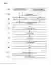
FIG. 1 a flowchart of the manufacture of a card body, and
FIG. 2 a cross section through a card body manufactured according to the method.
For the following description it will be assumed by way of example that a card body is being manufactured for a portable data carrier in the form of a chip card with conventional outer dimensions according to ISO standard 7810. However, the method can also be used in the same manner for manufacturing portable data carriers with other dimensions. For example, there can also be manufactured in the same manner portable data carriers in the SIM-card format or portable data carriers serving e.g. together with a housing as a USB stick.
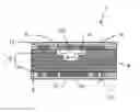
The method is illustrated as a flowchart in FIG. 1. It commences with a step 100 by making available two layers 2, 4 of synthetic paper with a thickness of 50 to 400 μm, designated in the Fig. as synth paper layers I and II. The synthetic paper is commercially available, industrial material as is offered e.g. by the company EMANAGREEN, Spain. It typically contains a content of 75 to 80 wt. % mineral powder, in particular calcium carbonate, as well as a content of 20 to 25 wt. % synthetic resin, e.g. high-density polyethylene (HDPE). The ratio of the constituents can vary somewhat, but a ratio of 3:1 is not fallen short of To the synthetic paper can be added small contents of further substances. Expediently, the synthetic paper is made available in sheet form or as a web. The two layers 2, 4 of synthetic paper later form the core structure 10 of a data carrier 1 to be manufactured, as is represented in FIG. 2.
In an expedient embodiment, at least one cover layer 6, 8 is furthermore made available, which can consist e.g. of PVC, step 102. The cover layer 6, 8 preferably consists of a biodegradable plastic, but can in a simple manner also consist of another common plastic, e.g. PVC. It has a thickness of 100 to 600 μm. When PVC or another poorly biodegradable plastic is used, the thickness of a cover layer 6, 8 should not exceed a value of 100 μm. Expediently, the cover layer 6, 8 is transparent.
In one variant, there are made available, as shown in FIG. 2, two cover layers 6, 8 which can consist of different materials and have different opacities. For example, one cover layer 6 can consist of PVC and be transparent, while the other cover layer 8 consists of PETG and is semitransparent. The cover layers 6, 8 can be made available as foils which are laminated with the other layers 2, 4. Alternatively, they can also be applied in the form of a lacquer layer, e.g. by a suitable printing method. If the finished data carrier 1 is to possess a magnetic strip, one of the cover layers 6, 8 is expediently equipped with a magnetic strip. The cover layers 6, 8 are optional. They can also be omitted.
In a step 104, a graphical pattern 12, 22 is respectively applied to one side of the layers 2, 4 of synthetic paper by a screen printing or offset printing process or by means of digital printing. The graphical pattern 12, 22 can comprise flat areas, structures and/or alphanumeric characters. The graphical patterns 12, 22 can be of different configuration. The printing step can be executed with conventional printing parameters and printing inks as are used for printing chip cards and credit cards.
In a step 106 there is applied to one, expediently to both, respectively other sides of the layers 2, 4 a thin film of an adhesive supporting the subsequent lamination. The adhesive 9 is preferably made available in the form of an adhesive lacquer. This form will be assumed in the further description. The application of the adhesive lacquer 9 is effected e.g. by screen printing, the thickness of the adhesive-lacquer layer lying below 5 μm. Without adhesive lacquer 9 the two layers 2, 4 would not adhere to each other sufficiently strongly. A suitable adhesive lacquer 9 is obtainable e.g. from the company Polynorma SA, Barcelona, E-08030 Spain, under the designation “Barniz Inter HV X3”.
The layers 2, 4 of synthetic paper and the cover layers 6, 8 are disposed one over the other in a sandwich arrangement in a subsequent step 108, so that the layers 2, 4 of synthetic paper between the cover layers 6, 8 and the sides of the layers 2, 4 printed with adhesive lacquer 9 lie against each other. When only one cover layer is present, the layers of synthetic paper are disposed under the cover layer in the same manner.
In this arrangement, the layers 2, 4, 6, 8 are laminated into a half-product in the following step 110. Laminating is done by a conventional laminating method for manufacturing chip cards and credit cards. This method comprises e.g. two heating steps and two cooling steps. The heating steps are effected at temperatures of 130 to 180° C. The pressure in the first heating step amounts to e.g. 10 to 20 bar at a heating time of 1 to 5 min and 60 to 100 bar at a reaction time of 10 to 20 min in the second heating step. The cooling steps are effected at ambient temperature and pressures of 60 to 160 bar. The cooling times lie between 1 and 10 min in the first step, between 5 and 20 min in the second step.
After the step 110 is performed there is obtained a planar, multilayer half-product which has at least a core structure 10 formed from two synthetic paper layers 2, 4 and respectively bearing a graphical pattern 12, 22 on the outer sides. The core structure 10 can moreover be covered on one or both sides with a transparent or translucent cover layer 6, 8. The surfaces 14, 24 of the half-product correspond to the final surfaces 14, 24 of the finished portable data carrier 1, except for a subsequent personalization and/or the incorporation of an IC.
In the following step 120, a card body having the final outer form intended for the data carrier 1 is separated from the planar half-product. Separation is expediently done by punching, but can also be done by cutting or milling.
In a subsequent step 130, hot-stamped elements can be applied to the card body by a conventional hot-stamping method.
If the portable data carrier to be manufactured is a chip card, steps 140, 142 are subsequently effected for creating a cavity in the card body and for inserting a chip module into the produced cavity. However, if the portable data carrier to be manufactured is for example a mere magnetic-strip card or a mere identification card without a microprocessor IC or magnetic strip, the steps 140, 142 are omitted.
The card body present thereafter is finally personalized in a step 150. This is done for example by applying personal data by a thermal transfer process and/or by notching; other per se known personalization methods can likewise be used.
FIG. 2 shows a cross section through data carrier 1 having a card body manufactured according to the method. The thicknesses of the individual layers and elements are not true to scale. The data carrier 1 consists of a core structure 10 which in turn consists of two layers 2, 4 of synthetic paper. The core structure 10 is furnished on both outwardly pointing sides with graphical patterns 12, 22. Over the graphical patterns 12, 22 there is respectively applied a transparent cover layer 6, 8 on both sides. In the upper layer 2 of synthetic paper there is formed a cavity 16 in which an IC module 20 is disposed. The IC module 20 is fixed by means of an adhesive 18 on the bottom and/or on other suitable supporting places of the cavity 16, e.g. on module shoulders formed between a wide and a narrower region of the cavity 16 as indicated in FIG. 2.
Without going beyond the basic idea according to the invention, the hereinabove described method permits a number of modifications and embodiments. In particular, there can be employed instead of two layers 2, 4 of synthetic paper only one such layer. Likewise, it is possible to employ three or more layers of synthetic paper. Over the cover layers 6, 8 there can also be respectively applied further layers. The separating step can further be effected with different separation techniques, e.g. by additional application of a laser or by prepunching the edge contour. The adhesive 9 can further also be made available in a different form from adhesive lacquer.
Claims
1-15. (canceled)
16. A method for manufacturing a multilayer card body for a portable data carrier having the following steps:
making available a first and a second layer of synthetic paper, the synthetic paper being based on calcium carbonate to which high-density polyethylene (HDPE) is added, the ratio amounting to at least 3 to 1 based on weight,
respectively printing a graphical pattern to one side of the layers of synthetic paper,
applying an adhesive lacquer to at least one side of one of the layers of synthetic paper,
bringing together the respectively one-sided printed layers of synthetic paper, so that the upper sides with the graphical pattern point outwardly and the side or sides coated with adhesive lacquer lie against each other, so that the adhesive lacquer lies between the layers of synthetic paper,
laminating the brought-together layers at a temperature of 120 to 180° C., and a pressure of 60 to 100 bar, into a half-product which has a core structure formed from two synthetic paper layers and respectively bearing a graphical pattern on the outer sides,
separating the card body from the half-product by means of a separating tool.
17. The method according to claim 16, wherein there is formed in the card body a cavity and therein an IC module is disposed, the cavity penetrating at least one synthetic paper layer of the core structure.
18. The method according to claim 16, wherein the layers of synthetic paper possess a thickness of 80 to 400 μm.
19. The method according to claim 16, wherein the adhesive lacquer is applied with a thickness of no more than 5 μm.
20. The method according to claim 16, wherein the graphical pattern is applied by a screen printing or an offset printing process.
21. The method according to claim 16, wherein the separation is effected by punching.
22. The method according to claim 16, wherein at least one cover layer is additionally disposed over the brought-together layers of synthetic paper and laminated as well.
23. The method according to claim 16, wherein the cover layer is a PVC foil.
24. The method according to claim 16, wherein the card body is hot-stamped.
25. A portable data carriers having a multilayer card body which bears a graphical pattern on at least one upper side, wherein the card body has a core structure formed from at least two layers of synthetic paper lying against each other only with the interposition of an adhesive lacquer, the synthetic paper being based on calcium carbonate to which high-density polyethylene (HDPE) is added, the ratio amounting to at least 3 to 1 based on weight.
26. The portable data carrier according to claim 25, wherein the layers of synthetic paper possess a thickness of 80 to 400 μm, and the thickness of the adhesive lacquer amounts to less than 5 μm.
27. The portable data carrier according to claim 25, wherein the card body has a cavity in which an IC module is disposed, the cavity extending into at least one of the layers of synthetic paper.
28. The portable data carrier according to claim 25, wherein the core structure is covered on one or both sides with a transparent or translucent cover layer.
Images & Drawings included:
Sources:
- United States Patent and Trademark Office - verify current appl. status at the USPTO↗
Similar patent applications:
- » 20230409861
Method for producing a card body, method for producing a chip card, card body for a chip card and chip card - » 20240001654
Multilayer Body, Card, Passport, Method for Producing Multilayer Body, Method for Producing Card, Method for Producing Passport, and Laser Marking Method - » 20250173540
CARD BODY WITH ABSORBENT CORE AND METHOD FOR PRODUCING A CARD BODY WITH ABSORBENT CORE - » 20190197384
Chip card body, chip card and method for producing a chip card body - » 20240111985
Chip body for a chip card, chip card, and method for producing a chip body - » 20140174645
Method for producing a card body - » 20110024511
Layered composite for a card body and method for producing the layered composite - » 20240037363
Method for producing a card body, card body for a chip card and chip card - » 20070172187
Optical sheet body and its producing method, optical card and composite memory - » 20240127023
Method for producing a chip card, card body for a chip card, and chip card
Recent applications in this class:
- » 20250292057 2025-09-18
SELF-CENTERED INLAY AND CORE LAYER FOR INFORMATION CARRYING CARD, PROCESS AND RESULTING PRODUCTS - » 20250272531 2025-08-28
WIRE EMBEDDED LABEL ON SPECIAL SUBSTRATE WITH OR WITHOUT INDUCTIVE COUPLING - » 20250265437 2025-08-21
COMBINATION RFID/EAS TAGS AND METHODS OF MANUFACTURE - » 20250252281 2025-08-07
TRANSACTION CARD INCORPORATING ALUMINUM ALLOYS - » 20250232150 2025-07-17
Easily Attachable RFID Tag and Method of Making the Same - » 20250209293 2025-06-26
METAL SMART CARD WITH RADIO-FREQUENCY ANTENNA AND METHOD FOR MANUFACTURING SUCH A SMART CARD - » 20250200321 2025-06-19
METAL SMARTCARD, AND METHOD FOR MANUFACTURING A METAL SMARTCARD - » 20250181878 2025-06-05
METHOD FOR PRODUCING A FILM FOR A CARD-SHAPED DATA CARRIER, FILM AND CARD-SHAPED DATA CARRIER - » 20250173540 2025-05-29
CARD BODY WITH ABSORBENT CORE AND METHOD FOR PRODUCING A CARD BODY WITH ABSORBENT CORE - » 20250156671 2025-05-15
PAYMENT CARDS WITH ACTIVATED INFORMATION DISPLAYS
Recent applications for this Assignee:
- » 20160321851 2016-11-03
Method and apparatus for handling value documents - » 20160292951 2016-10-06
Apparatus and method for checking value documents - » 20160232735 2016-08-11
Value document and method for checking the presence of the same - » 20160232730 2016-08-11
Method for checking a value document - » 20160217640 2016-07-28
Method and system for handling value documents - » 20160215456 2016-07-28
Value document and method for checking the presence of the same - » 20160110638 2016-04-21
Optically variable security element - » 20160094341 2016-03-31
Methods and system for secure communication between an RFID tag and a reader - » 20160080930 2016-03-17
Mobile device management - » 20160055358 2016-02-25
Check of a security element furnished with magnetic materials