LED module
US20150060935A1
2015-03-05
14/474,767
2014-09-02
✅ Patent granted
US 9,231,174 B2
2016-01-05
-
-
Victor A Mandala | Quovaunda V Jefferson
Novak Druce Connolly Bove + Quigg LLP
2034-09-02
Abstract:
An light emitting diode (LED) module includes a circuit board, a set of LED chips formed on and electrically connected to the circuit board, and an encapsulant arranged on the circuit board and covering the LED chips, a set of first recesses defined in a top surface of the encapsulant.
Inventors:
- CHUNG-MIN CHANG 21 🇹🇼 Hsinchu, Taiwan
- CHIEN-LIN CHANG-CHIEN 8 🇹🇼 Hsinchu, Taiwan
- YA-TING WU 4 🇹🇼 Hsinchu, Taiwan
- ZHENG-HUA YANG 3 🇹🇼 Hsinchu, Taiwan
Assignee:
- ADVANCED OPTOELECTRONIC TECHNOLOGY, INC. 432 🇹🇼 Hsinchu Hsien, Taiwan
Applicant:
Interested in similar patents?
Get notified when new applications in this technology area are published.
Classification:
H01L33/52 » CPC main
Semiconductor devices with at least one potential-jump barrier or surface barrier specially adapted for light emission; Processes or apparatus specially adapted for the manufacture or treatment thereof or of parts thereof; Details thereof characterised by the semiconductor body packages Encapsulations
H01L33/54 » CPC main
Semiconductor devices with at least one potential-jump barrier or surface barrier specially adapted for light emission; Processes or apparatus specially adapted for the manufacture or treatment thereof or of parts thereof; Details thereof characterised by the semiconductor body packages; Encapsulations having a particular shape
H01L25/0753 » CPC further
Assemblies consisting of a plurality of individual semiconductor or other solid state devices ; Multistep manufacturing processes thereof all the devices being of a type provided for in the same subgroup of groups - , e.g. assemblies of rectifier diodes the devices not having separate containers the devices being of a type provided for in group the devices being arranged next to each other
H01L2924/0002 » CPC further
Indexing scheme for arrangements or methods for connecting or disconnecting semiconductor or solid-state bodies as covered by; Technical content checked by a classifier Not covered by any one of groups , and
H01L27/00 IPC
Devices consisting of a plurality of semiconductor or other solid-state components formed in or on a common substrate
H01L25/075 IPC
Assemblies consisting of a plurality of individual semiconductor or other solid state devices ; Multistep manufacturing processes thereof all the devices being of a type provided for in the same subgroup of groups - , e.g. assemblies of rectifier diodes the devices not having separate containers the devices being of a type provided for in group
Description
CROSS-REFERENCE TO RELATED APPLICATIONS
This application claims priority to Chinese Patent Application No. 201310396038.0 filed on Sep. 4, 2013 in the State Intellectual Property Office Of The P. R. C, the contents of which are incorporated by reference herein.
FIELD
This disclosure relates to a light emitting diode (LED) module, and particularly to an integrated LED module.
BACKGROUND
Total reflection happens in the LED module, which decreases a light-extraction efficiency of the LED module.
BRIEF DESCRIPTION OF THE DRAWINGS
Implementations of the present technology will now be described, by way of example only, with reference to the attached figures.
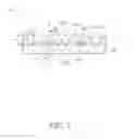
FIG. 1 is a cross-sectional diagrammatic view of an LED module in accordance with a first example embodiment of the present disclosure.
FIG. 2 is a diagrammatic view of the LED module of the present disclose.
FIG. 3 is a cross-sectional diagrammatic view of an LED module in accordance with a second example embodiment of the present disclosure.
FIG. 4 is a top plan view of an LED module in accordance with a third example embodiment of the present disclosure.
FIG. 5 is a top plan view of an LED module in accordance with a fourth example embodiment of the present disclosure.
FIG. 6 is a top plan view of an LED module in accordance with a fifth example embodiment of the present disclosure.
DETAILED DESCRIPTION OF EMBODIMENTS
It will be appreciated that for simplicity and clarity of illustration, numerous specific details are set forth in order to provide a thorough understanding of the embodiments described herein. However, it will be understood by those of ordinary skill in the art that the embodiments described herein can be practiced without these specific details. In other instances, methods, procedures and components have not been described in detail so as not to obscure the related relevant feature being described. In addition, the description is not to be considered as limiting the scope of the embodiments described herein. The drawings are not necessarily to scale and the proportions of certain parts have been exaggerated to better illustrate details and features of the present disclosure.
Referring to FIG. 1, a light emitting diode (LED) module 10 includes a circuit board 130, a set of LED chips 120 and an encapsulant 110. The circuit board 130 can be a circuit printed board, a ceramic base circuit board, a metal base circuit board, a fiberglass circuit board, a multilayer circuit board, a flexible circuit board, or other matter. The metal base circuit board can be an aluminum base circuit board, a copper base circuit board, or a base circuit board made of some other metal or other material. The LED chips 120 are arranged on and electrically connected to the circuit board 130. The LED chips 120 can be electrically connected to the circuit board 130 by flip-chip, wire bonding, or other means. The encapsulant 110 can be formed on the circuit board 130 and cover all or part of the LED chips 120.
A set of first recesses 111 are defined in the encapsulant 110. The first recesses 111 can be defined in a top surface 1101 of the encapsulant 110. A depth H′ of each first recess 111 is less than a thickness H of the encapsulant 110.
A pair of inclined surfaces 1111 is defined in each first recess 111. A first edge 201 and a second edge 202 are defined in each inclined surface 1111. A distance between the first edge 201 and the circuit board 130 is larger than that between the second edge 202 and the circuit board 130. Each inclined surface 1111 intersects on the top surface 1101 at the first edge 201. The two inclined surfaces 1111 of each first recess 111 intersect at the second edge 202.
A distance D between each first edge 201 and an optic axis O-O of a neighboring LED chip 120 is larger than zero, and less than or equal to a product of the thickness H of the encapsulant 110 and a tangent of a critical angle α of the encapsulant 110, which is 0<D≦H·tan α. A part of the light emitted from the LED chips 120 can reach the top surface 1101 of the encapsulant 110, and be refracted on the top surface 1101, then extract from the top surface 1101 to outside. In at least one embodiment (see FIG. 2), each LED chip 120 can be viewed as a point light source M. The top surface 1101 is parallel to the circuit board 130. An extracting angle of a light ray MB can be the critical angle α. When the light ray MB is just refracted on the top surface 1101 and extract from the top surface 1101 to outside, the distance D of the first edge 201 and the optic axis O-O of the neighboring LED chip 120 is equal between the product of the thickness H of the encapsulant 110 and the tangent of the critical angle α of the encapsulant 110, which is D=H·tan α.
An angle θ between a normal line I-I of each inclined surface 1111 and the optic axis O-O of the neighboring LED chip 120 is larger than or equal to a complement angle of the critical angle α of the encapsulant 110, and less than 90°, which is 90°−α≦θ<90°. A part of the light emitted from the LED chips can reach the inclined surface 1111 of the encapsulant 110, and be refracted on the inclined surface 1111, then extract from the inclined surface 1111 to outside. In at least one embodiment (see FIG. 2), an extracting angle of a light ray MC can be 90°. When the light ray MC is just refracted on the inclined surface 1111 and extract from the inclined surface 1111 to outside, the angle θ between the normal line I-I of each inclined surface 1111 and the optic axis O-O of the neighboring LED chip 120 is equal to the complement angle of the critical angle α of the encapsulant 110, which is θ=90°−α.
Referring to FIGS. 1 and 3-5, each first recess 111 is defined between two adjacent LED chips. In at least one embodiment, a cross section of each first recess 111 is V-shaped (see FIG. 1). In other embodiments, the cross section of each first recess 111 can be a trapezoid (see FIG. 3). A top view of the first recesses can be a cross-shaped (see FIGS. 4 and 5).
Referring to FIGS. 5 and 6, the first recesses 111 can be defined around the LED chips 120.
Referring to FIGS. 4 and 6, a set of second recesses 112 can be defined in gaps 300 between the first recesses 111. The second recesses 112 can be defined between the LED chips 120. Each second recess 112 can be a conical recess, a truncated conical recess, or other shape or size of recess.
The encapsulant 110 can include one or more photo luminescence properties (not shown). The photoluminescence properties can be provided by phosphor powder, fluorescent powder or other material. A refractive index of the encapsulant 110 can be in a range from 1.4 to 1.5.
In at least one embodiment, the refractive index of the encapsulant 110 can be 1.4. The critical angle α of the example encapsulant 110 is 45°. The distance D between each first edge 201 and the optic axis O-O of the neighboring LED chip 120 is larger than zero, and less than or equal to H tan 45°, which is 0<D≦H·tan 45°. An angle θ between a normal line I-I of each inclined surface 1111 and the optic axis O-O of the neighboring LED chip 120 is larger than or equal to a complement angle of the critical angle 45° of the encapsulant 110, and less than 90°, which is 45°≦θ<90°.
In at least one embodiment, the refractive index of the encapsulant 110 can be 1.5. The critical angle α of the example encapsulant 110 is 41° . The distance D between each first edge 201 and the optic axis O-O of the neighboring LED chip 120 is larger than zero, and less than or equal to H tan 41°, which is 0<D≦H·tan 41°. An angle θ between a normal line I-I of each inclined surface 1111 and the optic axis O-O of the neighboring LED chip 120 is larger than or equal to a complement angle of the critical angle 41° of the encapsulant 110, and less than 90°, which is 49°≦θ<90°.
It is to be further understood that even though numerous characteristics and advantages have been set forth in the foregoing description of embodiments, together with details of the structures and functions of the embodiments, the disclosure is illustrative only. Changes may be made in detail, including in matters of shape, size, and arrangement of parts within the principles of the disclosure to the full extent indicated by the broad general meaning of the terms in which the appended claims are expressed.
The embodiments shown and described above are only examples. Many details are often found in the art such as the other features of an LED module. Therefore, many such details are neither shown nor described. Even though numerous characteristics and advantages of the present technology have been set forth in the foregoing description, together with details of the structure and function of the present disclosure, the disclosure is illustrative only, and changes may be made in the detail, especially in matters of shape, size and arrangement of the parts within the principles of the present disclosure up to, and including the full extent established by the broad general meaning of the terms used in the claims. It will therefore be appreciated that the embodiments described above may be modified within the scope of the claims.
Claims
What is claimed is:1. A light emitting diode (LED) module comprising:
a circuit board;
a set of LED chips formed on and electrically connected to the circuit board; and
an encapsulant arranged on the circuit board and covering the LED chips, a set of first recesses defined in a top surface of the encapsulant.
2. The LED module of claim 1, wherein a depth of each recess is less than a thickness of the encapsulant.
3. The LED module of claim 2, wherein a pair of inclined surfaces is defined in each first recess.
4. The LED module of claim 3, wherein a first edge and a second edge are defined in each inclined surface, a distance between the first edge and the circuit board is larger than that between the second edge and the circuit board.
5. The LED module of claim 4, wherein each inclined surface intersects on the top surface at the first edge.
6. The LED module of claim 5, wherein the two inclined surfaces of each first recess intersect at the second edge.
7. The LED module of claim 6, wherein a distance between each first edge and an optic axis of a neighboring LED chip is larger than zero, and less than or equal to a product of the thickness of the encapsulant and a tangent of a critical angle of the encapsulant.
8. The LED module of claim 6, wherein an angle between a normal line of each inclined surface and the optic axis of the neighboring LED chip is larger than or equal to a complement angle of the critical angle of the encapsulant, and less than 90°.
9. The LED module of claim 2, wherein each first recess is defined between two adjacent LED chips.
10. The LED module of claim 9, wherein a cross section of each first recess is V-shaped.
11. The LED module of claim 10, wherein the first recesses are define around the LED chips.
12. The LED module of claim 11, wherein a top view of the first recesses is a cross-shaped.
13. The LED module of claim 9, wherein a cross section of each first recess is trapezoid.
14. The LED module of claim 1, wherein a set of second recesses are defined in gaps between the first recesses.
15. The LED module of claim 14, wherein the second recesses are defined between the LED chips.
16. The LED module of claim 15, each second recess is a conical recess or a truncated conical recess.
17. The LED module of claim 1, wherein the encapsulant comprises a plurality of photoluminescence properties.
18. The LED module of claim 17, wherein a refractive index of the encapsulant is in a range from 1.4 to 1.5.
Images & Drawings included:


Sources:
- United States Patent and Trademark Office - verify current appl. status at the USPTO↗
Similar patent applications:
- » 20070189007
LED mounting module, LED module, manufacturing method of LED mounting module, and manufacturing method of LED module - » 20160369983
Bendable LED module, circular LED module and wavy LED module - » 20240410553
PRINTED CIRCUIT BOARD FOR AN LED MODULE, LED MODULE, AND LED LIGHTS - » 20120294042
LED module, backlight unit including the LED module, and method for manufacturing the LED module - » 20120201026
LED Module, Method for Operating said LED Module and Lighting Device having said LED Module - » 20100270922
LED heat sink module, LED module for LED heat sink module - » 20230220960
LED base module, LED module, and LED lighting strip - » 20220260229
LED module, LED module and reflector arrangement, and vehicle headlamp - » 20160087176
Light emitting diode (LED) die module, LED element with the LED die module and method of manufacturing the LED die module - » 20090141490
Method for diminishing dark gap in arrayed led module, arrayed LED module, and imaging apparatus thereof
Recent applications in this class:
- » 20250056937 2025-02-13
ETCHED TRENCHES IN BOND MATERIALS FOR DIE SINGULATION, AND ASSOCIATED SYSTEMS AND METHODS - » 20250022991 2025-01-16
SEMICONDUCTOR PACKAGE - » 20240421269 2024-12-19
HIDDEN DISPLAY DEVICE AND METHOD OF MANUFACTURING THE SAME - » 20240266480 2024-08-08
METHOD OF MANUFACTURING LIGHT-EMITTING DEVICE INCLUDING STEP OF CURING SEALING MEMBER WHILE APPLYING CENTRIFUGAL FORCE - » 20240258472 2024-08-01
DISPLAY DEVICE AND MANUFACTURING METHOD THEREOF - » 20240250221 2024-07-25
Semiconductor package and manufacturing method of semiconductor package - » 20240234649 2024-07-11
LIGHT EMITTING DEVICE - » 20240170621 2024-05-23
DISPLAY DEVICE - » 20240136479 2024-04-25
LIGHT EMITTING DEVICE - » 20240097083 2024-03-21
Light emitting device having a dam surrounding a light emitting region and a barrier surrounding the dam
Recent applications for this Assignee:
- » 20220252938 2022-08-11
Light emitting diode device, backlight module, and liquid crystal display device having same - » 20220077345 2022-03-10
Back plate and method for fluid-assisted assembly of micro-LEDs thereon - » 20210359153 2021-11-18
Back plate and method for fluid-assisted assembly of micro-LEDs thereon - » 20200326594 2020-10-15
Optical lens, backlight module and display device using same - » 20190326489 2019-10-24
Light emitting diode package - » 20190319173 2019-10-17
Side-view light emitting diode package structure - » 20190140136 2019-05-09
Manufacturing method for light emitting diode crystal grains using adhesive layer on auxiliary substrate to fill gaps between light emitting diode crystal grains - » 20190103512 2019-04-04
Light emitting diode structure - » 20190033659 2019-01-31
Liquid crystal display device - » 20180212105 2018-07-26
Flip chip light emitting diode and method of manufacturing the same