Optoelectronic module and method for manufacturing the same
US20150115218A1
2015-04-30
14/482,942
2014-09-10
✅ Patent granted
US 9,312,658 B2
2016-04-12
-
-
Mark Prenty
Novak Druce Connolly Bove + Quigg LLP
2034-09-10
Abstract:
An optoelectronic module includes a substrate, an LED and a laser LED formed on the substrate, simultaneously. A method for manufacturing an optoelectronic module includes following steps: providing a sapphire substrate, and forming two adoped GaN layers, an N-type GaN layer, an active layer and a P-type GaN layer on the sapphire substrate in sequence; providing a substrate and forming a metallic adhering layer on the substrate; forming an ohmic contact layer and a reflecting layer on the P-type GaN layer in series; arranging the reflecting layer on the adhering layer; stripping the sapphire substrate and the two doped GaN layers from the N-type GaN layer to form a semiconductor structure; etching a top end of the semiconductor structure to divide the semiconductor structure into a laser LED region and an LED region; forming two N-type electrodes on the LED region and an LED region, respectively.
Inventors:
- YA-WEN LIN 37 🇹🇼 Hukou, Taiwan
- SHIH-CHENG HUANG 61 🇹🇼 Hukou, Taiwan
- PO-MIN TU 68 🇹🇼 Hukou, Taiwan
- PO-MIN TU 65 🇹🇼 Hsinchu, Taiwan
- SHIH-CHENG HUANG 73 🇹🇼 Hsinchu, Taiwan
- YA-WEN LIN 48 🇹🇼 Hsinchu, Taiwan
- CHING-HSUEH CHIU 22 🇹🇼 Hukou, Taiwan
- CHING-HSUEH CHIU 23 🇹🇼 Hsinchu, Taiwan
Assignee:
- ADVANCED OPTOELECTRONIC TECHNOLOGY, INC. 432 🇹🇼 Hsinchu Hsien, Taiwan
Applicant:
Interested in similar patents?
Get notified when new applications in this technology area are published.
Classification:
H01L2933/0058 » CPC further
Details relating to devices covered by the group but not provided for in its subgroups; Processes relating to semiconductor body packages relating to optical field-shaping elements
H01S5/125 » CPC further
Semiconductor lasers; Construction or shape of the optical resonator, e.g. extended or external cavity, coupled cavities, bent-guide, varying width, thickness or composition of the active region the resonator having a periodic structure, e.g. in distributed feedback [DFB] lasers Distributed Bragg reflector [DBR] lasers
H01L33/06 » CPC further
Semiconductor devices with at least one potential-jump barrier or surface barrier specially adapted for light emission; Processes or apparatus specially adapted for the manufacture or treatment thereof or of parts thereof; Details thereof characterised by the semiconductor bodies with a quantum effect structure or superlattice, e.g. tunnel junction within the light emitting region, e.g. quantum confinement structure or tunnel barrier
H01L33/32 » CPC further
Semiconductor devices with at least one potential-jump barrier or surface barrier specially adapted for light emission; Processes or apparatus specially adapted for the manufacture or treatment thereof or of parts thereof; Details thereof characterised by the semiconductor bodies; Materials of the light emitting region containing only elements of group III and group V of the periodic system containing nitrogen
H01L33/10 » CPC further
Semiconductor devices with at least one potential-jump barrier or surface barrier specially adapted for light emission; Processes or apparatus specially adapted for the manufacture or treatment thereof or of parts thereof; Details thereof characterised by the semiconductor bodies with a light reflecting structure, e.g. semiconductor Bragg reflector
H01S5/343 IPC
Semiconductor lasers; Structure or shape of the active region; Materials used for the active region comprising quantum well or superlattice structures, e.g. single quantum well lasers [SQW-lasers], multiple quantum well lasers [MQW-lasers] or graded index separate confinement heterostructure lasers [GRINSCH-lasers] in AB compounds, e.g. AlGaAs-laser, InP-based laser
H01S5/34333 » CPC further
Semiconductor lasers; Structure or shape of the active region; Materials used for the active region comprising quantum well or superlattice structures, e.g. single quantum well lasers [SQW-lasers], multiple quantum well lasers [MQW-lasers] or graded index separate confinement heterostructure lasers [GRINSCH-lasers] in AB compounds, e.g. AlGaAs-laser, InP-based laser with a well layer based on Ga(In)N or Ga(In)P, e.g. blue laser
H01S5/026 » CPC main
Semiconductor lasers; Structural details or components not essential to laser action Monolithically integrated components, e.g. waveguides, monitoring photo-detectors, drivers
H01L27/15 » CPC further
Devices consisting of a plurality of semiconductor or other solid-state components formed in or on a common substrate including semiconductor components with at least one potential-jump barrier or surface barrier specially adapted for light emission
H01S5/10 IPC
Semiconductor lasers Construction or shape of the optical resonator, e.g. extended or external cavity, coupled cavities, bent-guide, varying width, thickness or composition of the active region
H01L33/405 » CPC further
Semiconductor devices with at least one potential-jump barrier or surface barrier specially adapted for light emission; Processes or apparatus specially adapted for the manufacture or treatment thereof or of parts thereof; Details thereof characterised by the electrodes; Materials therefor Reflective materials
H01S5/0213 » CPC further
Semiconductor lasers; Structural details or components not essential to laser action; Substrates, e.g. growth, shape, material, removal or bonding; Sapphire, quartz or diamond based substrates
H01S5/02 IPC
Semiconductor lasers Structural details or components not essential to laser action
H01L33/40 IPC
Semiconductor devices with at least one potential-jump barrier or surface barrier specially adapted for light emission; Processes or apparatus specially adapted for the manufacture or treatment thereof or of parts thereof; Details thereof characterised by the electrodes Materials therefor
Description
FIELD
The present disclosure generally relates to an optoelectronic module and a method for manufacturing the optoelectronic module.
BACKGROUND
A typical optoelectronic integrated circuit includes a plurality of LEDs and laser LEDs to emit different signals. However, the LEDs and the laser LEDs are independent and spaced from each other. The LEDs and laser LEDs may occupy too much area on the optoelectronic integrated module.
BRIEF DESCRIPTION OF THE DRAWINGS
Implementations of the present technology will now be described, by way of example only, with reference to the attached figures.
FIG. 1 is a cross sectional view of an optoelectronic module according to an exemplary embodiment of the present disclosure.
FIG. 2 is a schematic view showing a first step of a method for manufacturing the optoelectronic module of FIG. 1.
FIG. 3 is a schematic view showing a second step of a method for manufacturing the optoelectronic module of FIG. 1.
FIG. 4 is a schematic view showing a third step of a method for manufacturing the optoelectronic module of FIG. 1.
FIG. 5 is a schematic view showing a fourth step of a method for manufacturing the optoelectronic module of FIG. 1.
FIGS. 6-7 is a schematic view showing a fifth step of a method for manufacturing the optoelectronic module of FIG. 1.
FIGS. 6-7 is a schematic view showing a fifth step of a method for manufacturing the optoelectronic module of FIG. 1.
FIG. 8 shows nano poles of the optoelectronic module in this embodiment.
FIG. 9 shows nano poles of the optoelectronic module in an alternative embodiment.
FIG. 10 is a schematic view showing a sixth step of a method for manufacturing the optoelectronic module of FIG. 1.
DETAILED DESCRIPTION
It will be appreciated that for simplicity and clarity of illustration, where appropriate, reference numerals have been repeated among the different figures to indicate corresponding or analogous elements. In addition, numerous specific details are set forth in order to provide a thorough understanding of the embodiments described herein. However, it will be understood by those of ordinary skill in the art that the embodiments described herein can be practiced without these specific details. In other instances, methods, procedures, and components have not been described in detail so as not to obscure the related relevant feature being described. Also, the description is not to be considered as limiting the scope of the embodiments described herein. The drawings are not necessarily to scale and the proportions of certain parts have been exaggerated to better illustrate details and features of the present disclosure.
The term “comprising,” when utilized, means “including, but not necessarily limited to”; it specifically indicates open-ended inclusion or membership in the so-described combination, group, series and the like.
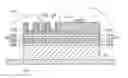
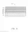
Referring to FIG. 1, an optoelectronic module in accordance with an exemplary embodiment of the disclosure includes a substrate 10, a laser LED 30 and an LED 50 formed on the substrate 10, simultaneously. The LED 30 is located at a side of the laser LED 50 and is spaced from the laser LED 50. The substrate 10 is an electrically insulating layer and mounted on an optoelectronic integrated circuit 60.
The LED 50 includes an adhering layer 20a, a reflecting layer 18a, an ohmic contact layer 17a, a P-type GaN layer 16a, an active layer 15a, an un-etched N-type GaN layer 14a formed on substrate 10 in series, and an N-type electrode 41a formed on the N-type GaN layer 14a. The laser LED 30 includes an adhering layer 20b, a reflecting layer 18b, an ohmic contact layer 17b, a P-type GaN layer 16b, an active layer 15b, an etched N-type GaN layer 14b formed on the substrate 10 in series, and an N-type electrode 41b formed on the N-type GaN layer 14b.
A method for manufacturing the optoelectronic module includes following steps:
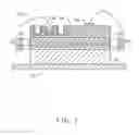
Referring to FIG. 2, the first step is providing a sapphire substrate 11, and forming a doped GaN layer 12 under low temperature, a doped GaN layer 13 under high temperature, an N-type GaN layer 14, an active layer 15 and a P-type GaN layer 16 on the sapphire substrate 11 in sequence from bottom to top.
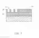
Referring to FIG. 3, the second step is providing the substrate 10 and forming a metallic adhering layer 20 on the substrate 10 by plating; forming an ohmic contact layer 17 and a reflecting layer 18 on the P-type GaN layer 16 in series. The reflecting layer 18 is a metallic layer or a bragg reflection layer. In this embodiment, the reflecting layer 18 is a bragg reflection layer.
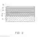
Referring to FIG. 4, the third step is arranging the reflecting layer 18 on the adhering layer 20 and pressing the reflecting layer 18 to the adhering layer 20 by 3000 to 7000 N under 200 to 400 degrees Celsius to make the reflecting layer 18 be bonded on the adhering layer 20. Preferably, the reflecting layer 18 is pressed by 6000 N under 300 degrees Celsius.
Referring to FIG. 5, the fourth step is stripping the sapphire substrate 11, the doped GaN layer 12 and the doped GaN layer 13 from the N-type GaN 14. Thus, a semiconductor structure 21 is obtained which comprising the substrate 10, the adhering layer 20, the reflecting layer 18, the ohmic contact layer 17, the P-type GaN layer 16, the active layer 15 and the N-type GaN layer 14. The adhering layer 20, the reflecting layer 18, the ohmic contact layer 17, the P-type GaN layer 16, the active layer 15 and the N-type GaN layer 14 are formed on the substrate 10 in series.
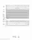
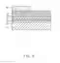
Referring to FIGS. 6-7, the fifth step is etching a top end of the semiconductor structure 21 to divide the semiconductor structure 21 into a laser LED region 25 and an LED region 27.
Specifically, forming a photoresist layer 28 on a left side of a top surface of the N-type GaN layer 14 and etching the photoresist layer 28 to divide the photoresist layer 28 into a plurality of spaced photoresist portions and then etching the semiconductor structure 21 along the space between the photoresist portions until a top end of the left side of the N-type GaN layer 14 is etched to form a plurality of nano poles 23, and then taking off the photoresist portions. The photoresist layer 28 is etched by acid solution or irradiation of yellow light. A middle of the semiconductor structure 21 is etched along a height direction of the semiconductor structure 21 to a top end of the substrate 10 to form a gap 80. The gap 80 separates a left part having the nano poles 23, which is the laser LED region 25, from a right part having no nano poles 23, which is the LED region 27. A bottom portion of the left side of the N-type GaN layer 14 which is not etched is configured as a support portion 29 to support the nano poles 23. The nano poles 23 extend from a top surface of the supporting portion 29.
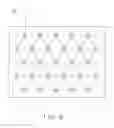
Referring to FIG. 8, each nano pole 23 is cylindrical and a diameter thereof is varied between 20 nanometer to 100 nanometer. Preferably, the diameter of each nano pole 23 is 50 nanometer. A height of each nano pole 23 is varied between 100 nanometer to 500 nanometer. Preferably, the height of each nano pole 23 is 200 nanometer. The nano poles 23 are spaced from each other. A distance between each two adjacent nano poles 23 is varied between 50 nanometer to 500 nanometer. Preferably, the distance is 200 nanometer. The nano poles 23 are arranged regular, for example, as shown in FIG. 8, the nano poles 23 are arranged to define a plurality of connected hexagons and each hexagon has one nano pole 23 acting as a central thereof; as shown in FIG. 9, in an alternative embodiment, the nano poles 23 can be arranged in matrix to define a plurality of rectangles.
Referring to FIG. 10, the sixth step is coating a metallic film 40 on the nano poles 23 and the exposed part of the top surface of the support portion 29.
Referring to FIG. 1 again, the seventh step is etching a part of the metallic film 40 located at any two adjacent nano poles 23 to expose the supporting portion 29, and forming the N-type electrode 41b on the exposed supporting portion 29, and the N-type electrode 41a on a top end of the LED region 27, and bonding wires 43 on the N-type electrodes 41a, 41b, respectively. In this state, the optoelectronic module is manufactured completely.
The embodiments shown and described above are only examples. Therefore, many such details are neither shown nor described. Even though numerous characteristics and advantages of the present technology have been set forth in the foregoing description, together with details of the structure and function of the present disclosure, the disclosure is illustrative only, and changes may be made in the detail, including in matters of shape, size, and arrangement of the parts within the principles of the present disclosure, up to and including the full extent established by the broad general meaning of the terms used in the claims. It will therefore be appreciated that the embodiments described above may be modified within the scope of the claims.
Claims
What is claimed is:1. An optoelectronic module comprising:
a substrate; and
an LED and a laser LED simultaneously placed on the substrate.
2. The optoelectronic module of claim 1, wherein the LED is located at a side of the laser LED and is spaced from the laser LED.
3. The optoelectronic module of claim 1, wherein the LED comprises an adhering layer, a reflecting layer, an ohmic contact layer, a P-type GaN layer, an active layer, an un-etched N-type GaN layer formed on the substrate in series, the laser LED comprises an adhering layer, a reflecting layer, an ohmic contact layer, a P-type GaN layer, an active layer, and an etched N-type GaN layer formed on the substrate in series, a top end of the N-type GaN layer of the laser LED being etched to form a plurality of nano poles.
4. The optoelectronic module of claim 3, wherein each nano pole is cylindrical and a diameter thereof is varied between 20 nanometer to 100 nanometer.
5. The optoelectronic module of claim 4, wherein the diameter of each nano pole is 50 nanometer.
6. The optoelectronic module of claim 3, wherein the nano poles are spaced from each other.
7. The optoelectronic module of claim 6, wherein a distance between each two adjacent nano poles is varied between 50 nanometer to 500 nanometer.
8. The optoelectronic module of claim 3, wherein a height of each nano pole is varied between 100 nanometer to 500 nanometer.
9. The optoelectronic module of claim 3, wherein the nano poles are arranged regular.
10. The optoelectronic module of claim 3, wherein a gap is defined between the LED and the laser LED to separate the adhering layer, the reflecting layer, the ohmic contact layer, the P-type GaN layer, the active layer, the un-etched N-type GaN layer of the LED from the adhering layer, the reflecting layer, the ohmic contact layer, the P-type GaN layer, the active layer, and the etched N-type GaN layer of the laser LED.
11. A method for manufacturing an optoelectronic module comprising following steps:
providing a sapphire substrate, and forming a doped GaN layer under low temperature, a doped GaN layer under high temperature, an N-type GaN layer, an active layer and a P-type GaN layer on the sapphire substrate in sequence from bottom to top;
providing a substrate and forming a metallic adhering layer on the substrate by plating;
forming an ohmic contact layer and a reflecting layer on the P-type GaN layer in series;
arranging the reflecting layer on the adhering layer;
stripping the sapphire substrate and the two doped GaN layers from the N-type GaN layer to form a semiconductor structure;
etching a top end of the semiconductor structure to divide the semiconductor structure into a laser LED region and an LED region; and
forming two N-type electrodes on the LED region and an LED region, respectively.
12. The optoelectronic module of claim 11, wherein a top end of the N-type GaN layer of the laser region is etched to form a plurality of nano poles thereon.
13. The optoelectronic module of claim 12, wherein the nano poles are coated by a metallic film.
14. The optoelectronic module of claim 11, wherein the reflecting layer is a bragg reflection layer.
15. The optoelectronic module of claim 11, wherein the reflecting layer is pressed by 3000 to 7000 N under 200 to 400 degrees Celsius to make the reflecting layer be bonded on the adhering layer.
16. The optoelectronic module of claim 15, wherein the reflecting layer is pressed by 6000 N under 300 degrees Celsius.
Images & Drawings included:


Sources:
- United States Patent and Trademark Office - verify current appl. status at the USPTO↗
Similar patent applications:
- » 20060039658
Optoelectronic conversion header, LSI package with interface module, method of manufacturing optoelectronic conversion header, and optical interconnection system - » 20070009212
OPTOELECTRONIC MODULE AND MANUFACTURING METHOD OF SAID MODULE - » 20140068924
Method for manufacturing optoelectronic module - » 10357854
Optoelectronic modules and methods of manufacturing the same - » 20180204959
Optoelectronic modules and methods for manufacturing the same - » 20200127147
Optoelectronic module assembly and manufacturing method - » 20240142728
OPTICAL COMPONENT, OPTOELECTRONIC MODULE AND METHOD OF MANUFACTURE - » 20190088801
Optoelectronic module assembly and manufacturing method - » 20070069317
Optoelectronics processing module and method for manufacturing thereof - » 20050041935
Optoelectronics processing module and method for manufacturing thereof
Recent applications in this class:
- » 20250279625 2025-09-04
HYBRID INTERGRATED LASER HAVING A SILICON PHOTONIC COUPLER MATCHED TO A PHOTONIC INTEGRATED CIRCUIT - » 20250246875 2025-07-31
CIRCUIT AND SYSTEM FOR DRIVING INTEGRATED SEMICONDUCTOR LASER DEVICE - » 20250246874 2025-07-31
OPTICAL CHIP FOR FIBER EDGE COUPLING AND/OR ACTIVE PHOTONICS INTEGRATION - » 20250174963 2025-05-29
INTEGRATED DENSE WAVELENGTH DIVISION MULTIPLEXED LASER ARRAY - » 20250141182 2025-05-01
SEMICONDUCTOR INTEGRATED OPTICAL DEVICE - » 20250141181 2025-05-01
FREQUENCY-CHIRPED SILICON PHOTONIC LASERS - » 20250055253 2025-02-13
Wavelength Multiplex Light Source - » 20240364074 2024-10-31
LASER DEVICE AND METHOD OF MANUFACTURING THE SAME - » 20240356303 2024-10-24
PHOTONIC INTEGRATED CIRCUIT DEVICE AND FABRICATION METHOD OF THE SAME - » 20240348006 2024-10-17
SILICON PHOTONIC SYMMETRIC DISTRIBUTED FEEDBACK LASER
Recent applications for this Assignee:
- » 20220252938 2022-08-11
Light emitting diode device, backlight module, and liquid crystal display device having same - » 20220077345 2022-03-10
Back plate and method for fluid-assisted assembly of micro-LEDs thereon - » 20210359153 2021-11-18
Back plate and method for fluid-assisted assembly of micro-LEDs thereon - » 20200326594 2020-10-15
Optical lens, backlight module and display device using same - » 20190326489 2019-10-24
Light emitting diode package - » 20190319173 2019-10-17
Side-view light emitting diode package structure - » 20190140136 2019-05-09
Manufacturing method for light emitting diode crystal grains using adhesive layer on auxiliary substrate to fill gaps between light emitting diode crystal grains - » 20190103512 2019-04-04
Light emitting diode structure - » 20190033659 2019-01-31
Liquid crystal display device - » 20180212105 2018-07-26
Flip chip light emitting diode and method of manufacturing the same