Apparatus and method for placing and mounting solder balls on an integrated circuit substrate
US20150122873A1
2015-05-07
14/069,453
2013-11-01
✅ Patent granted
US 9,120,170 B2
2015-09-01
-
-
Kiley Stoner
Alan D. Kamrath | Kamrath IP Lawfirm, P.A.
2033-11-01
Abstract:
An apparatus for placing and mounting solder balls on an integrated circuit substrate contains: a fixture, a vacuuming device, a guiding plate, and a storage tank. The fixture includes a plurality of first grooves defined therein, the vacuuming device is disposed over the fixture and includes a vacuum chamber which has an air pore so that when air is drawn out of the vacuum chamber via the air pore, a plurality of solder balls are attached, and when the air is fed into the vacuum chamber from the air pore, the plurality of solder balls are released. The guiding plate is secured below the fixture, and the storage tank is arranged below the guiding plate and is applied to accommodate the plurality of solder balls. Thereby, a production yield of placing and mounting the plurality of solder balls on an integrated circuit substrate is enhanced.
Assignee:
- Zen Voce Corporation 1 🇹🇼 Sinfong Township, Taiwan
Applicant:
Interested in similar patents?
Get notified when new applications in this technology area are published.
Classification:
B23K3/0623 » CPC main
Tools, devices, or special appurtenances for soldering, e.g. brazing, or unsoldering, not specially adapted for particular methods; Solder feeding devices; Solder melting pans; Solder feeding devices for shaped solder piece feeding, e.g. preforms, bumps, balls, pellets, droplets
H01L24/742 » CPC further
Arrangements for connecting or disconnecting semiconductor or solid-state bodies; Methods or apparatus related thereto; Apparatus for manufacturing arrangements for connecting or disconnecting semiconductor or solid-state bodies; Apparatus for manufacturing means for bonding, e.g. connectors Apparatus for manufacturing bump connectors
B23K3/06 IPC
Tools, devices, or special appurtenances for soldering, e.g. brazing, or unsoldering, not specially adapted for particular methods Solder feeding devices; Solder melting pans
H01L23/00 IPC
Details of semiconductor or other solid state devices
B23K31/02 IPC
Processes relevant to this subclass, specially adapted for particular articles or purposes, but not covered by only one of the preceding main groups relating to soldering or welding
Description
FIELD OF THE INVENTION
The present invent relates to an apparatus and a method for placing and mounting solder balls on an integrated circuit substrate which prevent a plurality of solder balls from being scraped so as to enhances production yield.
BACKGROUND OF THE INVENTION
A conventional method for mounting solder balls on an integrated circuit substrate contains: a first fixture including a plurality of grooves, and each groove has an upper opening and a lower opening smaller than the upper opening and is served to receive a solder ball. A through hole is defined below a respective one of the plurality of grooves, and a vacuuming device is fixed below the first fixture and includes a vacuuming device formed therein and having a plurality of connecting orifices for corresponding to a plurality of through holes of the first fixture, the vacuuming chamber also has an air pore defined on a central portion thereof so that when air is drawn out of the vacuum chamber via the air pore, a plurality of solder balls are attached, and when air is fed into the vacuum chamber from the air pore, the plurality of solder balls are released. A turning assembly is mounted on two side of the vacuuming device so as to rotate the first fixture 180 degrees. A guiding plate is disposed below the first fixture and includes a plurality of apertures for corresponding to the plurality of grooves of the first fixture, each aperture is provided to hold the solder ball. A second fixture is secured above the guiding plate and is applied to accommodate the plurality of solder balls. In operation, the guiding plate is descended to connect with the first fixture, and the turning device rotates the first fixture and the guiding plate so that the second fixture moves back and forth on the guiding plate, hence the plurality of solder balls are placed into the plurality of grooves of the first fixture via the plurality of apertures of the guiding plate, and then the vacuuming device draws air out of the vacuum chamber through the air pore so that the plurality of solder balls are attached. Thereafter, the guiding plate is lifted to move away from the first fixture on the first fixture, and the turning device downwardly rotate the first fixture 180 degrees so that the plurality of solder balls on the first fixture face downwardly. A substrate is lifted, and air is fed into the vacuum chamber from the air pore so that the plurality of solder balls are released from the first fixture and are mounted onto a flux of the substrate, and then the substrate is moved downwardly, thereby finishing a ball mounting process.
However, a gap between the second fixture and the guiding plate cannot be controlled exactly, so such a conventional method is only applicable for each solder ball with more than 0.25 mm of size, and the plurality of solder balls are scraped easily in a ball placing process.
The present invention has arisen to mitigate and/or obviate the afore-described disadvantages.
SUMMARY OF THE INVENTION
The primary object of the present invention is to provide an apparatus and a method for placing and mounting solder balls on an integrated circuit substrate which prevent a plurality of solder balls from being scraped so as to enhance production yield.
To obtain the above objective, an apparatus for placing and mounting solder balls on an integrated circuit substrate comprising: a fixture, a vacuuming device, a guiding plate, and a storage tank.
The fixture includes a plurality of first grooves defined therein, and each first groove has an upper opening and a lower opening, a diameter of the upper opening is less than that of the lower opening, and each first groove is provided to receive a respective one of a plurality of solder balls, and the fixture also includes a plurality of through holes formed therein and located on the plurality of first grooves.
The vacuuming device is disposed over the fixture and includes a vacuum chamber arranged therein and having a plurality of connecting orifices for corresponding to the plurality of through holes of the fixture, the vacuum chamber has an air pore defined on a central portion thereof so that when air is drawn out of the vacuum chamber via the air pore, the plurality of solder balls are attached, and when the air is fed into the vacuum chamber from the air pore, the plurality of solder balls are released, the vacuuming device includes a turning assembly fixed on two sides thereof so as to leftward or rightward rotate the fixture, the vacuuming device, the guiding plate, and the storage tank over 180 degrees.
The guiding plate is secured below the fixture and includes a plurality of apertures for corresponding to the plurality of first grooves of the fixture, and each aperture is used to receive the respective one of the plurality of solder balls, the guiding plate also includes a plurality of second grooves defined therein and communicating with the plurality of apertures, and a diameter of a lower opening of each second groove is greater than that of each aperture.
The storage tank is arranged below the guiding plate and is applied to accommodate the plurality of solder balls.
In addition, a method for placing and mounting solder balls on an integrated circuit substrate comprises steps of:
-
- A. lifting a guiding plate and a storage tank upwardly to connect with a fixture;
- B. rotating a turning assembly counterclockwisely, after the guiding plate and the storage tank are connected with the fixture;
- C. drawing air out of the vacuum chamber via an air pore by means of a vacuuming device so as to attach a plurality of solder balls, when the turning assembly rotates counterclockwisely, wherein after the turning assembly rotates counterclockwisely over 180 degrees, the plurality of solder balls in the storage tank move leftward;
- D. rotating the turning assembly clockwisely after the plurality of solder balls in the storage tank move leftward;
- E. moving the plurality of solder balls in storage tank rightward after the turning assembly rotates clockwisely over 180 degrees;
- F. placing the plurality of solder balls into a plurality of apertures of the guiding plate from the storage tank again and rotating the storage tank, the guiding plate, the vacuuming device, and the fixture back to an original angle;
- G. moving the guiding plate and the storage tank downwardly so that the guiding plate and the storage tank disconnect from the fixture;
- H. horizontally moving the guiding plate and the storage to one side;
- I. lifting a substrate;
- J. starting to mount the plurality of solder balls;
- K. re-feeding air into the vacuum chamber from the air pore of the vacuuming device so as to release the plurality of solder balls onto a flux of the substrate from the fixture;
- L. descending the substrate on which the plurality of solder balls are mounted.
BRIEF DESCRIPTION OF THE DRAWINGS
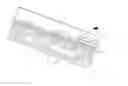
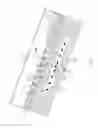
FIG. 1 is a cross sectional view showing the assembly of an apparatus for placing and mounting solder balls on an integrated circuit substrate according to a preferred embodiment of the present invention.
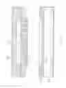
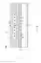
FIG. 2 is a cross sectional view showing the operation of step A of a method for placing and mounting solder balls on an integrated circuit substrate according to a preferred embodiment of the present invention.
FIG. 3 is a cross sectional view showing the operation of step B of the method for placing and mounting solder balls on an integrated circuit substrate according to the preferred embodiment of the present invention.
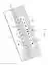
FIG. 4 is a cross sectional view showing the operation of step C of the method for placing and mounting solder balls on an integrated circuit substrate according to the preferred embodiment of the present invention.
FIG. 5 is a cross sectional view showing after the turning assembly rotates counterclockwisely over 180 degrees, a plurality of solder balls in the storage tank move leftward.
FIG. 6 is a cross sectional view showing the operation of step D of the method for placing and mounting solder balls on an integrated circuit substrate according to the preferred embodiment of the present invention.
FIG. 7 is a cross sectional view showing the operation of step E of the method for placing and mounting solder balls on an integrated circuit substrate according to the preferred embodiment of the present invention.
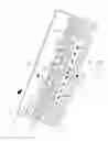
FIG. 8 is a cross sectional view showing the operation of step F of the method for placing and mounting solder balls on an integrated circuit substrate according to the preferred embodiment of the present invention.
FIG. 9 is a cross sectional view showing the operation of step G of the method for placing and mounting solder balls on an integrated circuit substrate according to the preferred embodiment of the present invention.
FIG. 10 is a cross sectional view showing the operation of step H of the method for placing and mounting solder balls on an integrated circuit substrate according to the preferred embodiment of the present invention.
FIG. 11 is a cross sectional view showing the operation of step I of the method for placing and mounting solder balls on an integrated circuit substrate according to the preferred embodiment of the present invention.
FIG. 12 is a cross sectional view showing the operation of step J of the method for placing and mounting solder balls on an integrated circuit substrate according to the preferred embodiment of the present invention.
FIG. 13 is a cross sectional view showing the operation of step K of the method for placing and mounting solder balls on an integrated circuit substrate according to the preferred embodiment of the present invention.
FIG. 14 is a cross sectional view showing the operation of step L of the method for placing and mounting solder balls on an integrated circuit substrate according to the preferred embodiment of the present invention.
DETAILED DESCRIPTION OF THE PREFERRED EMBODIMENTS
With reference to FIG. 1, an apparatus for placing and mounting solder balls on an integrated circuit substrate according to a preferred embodiment of the present invention comprises: a fixture 10, a vacuuming device 20, a guiding plate 30, and a storage tank 40.
The fixture 10 includes a plurality of first grooves 11 defined therein, and each first groove 11 has an upper opening and a lower opening, wherein a diameter of the upper opening is less than that of the lower opening, and each first groove 11 is provided to receive a respective one of a plurality of solder balls 1, and the fixture 10 also includes a plurality of through holes 12 formed therein and located on the plurality of first grooves 11.
The vacuuming device 20 is disposed over the fixture 10 and includes a vacuum chamber 21 arranged therein and having a plurality of connecting orifices 22 for corresponding to the plurality of through holes 12 of the fixture 10, the vacuum chamber 21 has an air pore 23 defined on a central portion thereof so that when air is drawn out of the vacuum chamber 21 via the air pore 23, the plurality of solder balls 1 are attached, and when the air is fed into the vacuum chamber 21 from the air pore 23, the plurality of solder balls 1 are released. The vacuuming device 20 includes a turning assembly 24 fixed on two sides thereof so as to leftward or rightward rotate the fixture 10, the vacuuming device 20, the guiding plate 30, and the storage tank 40 over 180 degrees.
The guiding plate 30 is secured below the fixture 10 and includes a plurality of apertures 31 for corresponding to the plurality of first grooves 11 of the fixture 10, and each aperture 31 is used to receive the respective one of the plurality of solder balls 1. The guiding plate 30 also includes a plurality of second grooves 32 defined therein and communicating with the plurality of apertures 31, and wherein a diameter of a lower opening of each second groove 32 is greater than that of each aperture 31.
The storage tank 40 is arranged below the guiding plate 30 and is applied to accommodate the plurality of solder balls 1.
A method for placing and mounting solder balls on an integrated circuit substrate according to a preferred embodiment of the present invention comprises steps of:
-
- A. lifting a guiding plate 30 and a storage tank 40 upwardly to connect with a fixture 10 (as shown in FIG. 2);
- B. rotating a turning assembly 24 counterclockwisely, after the guiding plate 30 and the storage tank 40 are connected with the fixture 10 (as illustrated in FIG. 3);
- C. drawing air out of the vacuum chamber 21 via an air pore 23 by means of a vacuuming device 20 so as to attach a plurality of solder balls 1, when the turning assembly 24 rotates counterclockwisely (as shown in FIG. 4), wherein after the turning assembly 24 rotates counterclockwisely over 180 degrees, the plurality of solder balls 1 in the storage tank 40 move leftward (as illustrated in FIG. 5);
- D. rotating the turning assembly 24 clockwisely after the plurality of solder balls 1 in the storage tank 40 move leftward (as shown in FIG. 6);
- E. moving the plurality of solder balls 1 in storage tank 40 rightward after the turning assembly 24 rotates clockwisely over 180 degrees (as illustrated in FIG. 7);
- F. placing the plurality of solder balls 1 into a plurality of apertures 31 of the guiding plate 30 from the storage tank 40 again and rotating the storage tank 40, the guiding plate 30, the vacuuming device 20, and the fixture 10 back to an original angle (as shown in FIG. 8);
- G. moving the guiding plate 30 and the storage tank 40 downwardly so that the guiding plate 30 and the storage tank 40 disconnect from the fixture 10 (as illustrated in FIG. 9);
- H. horizontally moving the guiding plate 30 and the storage 40 to one side (as illustrated in FIG. 10);
- I. lifting a substrate 50 (as shown in FIG. 11);
- J. starting to mount the plurality of solder balls 1 (as illustrated in FIG. 12);
- K. re-feeding air into the vacuum chamber 21 from the air pore 23 of the vacuuming device 20 so as to release the plurality of solder balls 1 onto a flux 51 of the substrate 50 from the fixture 10 (as shown in FIG. 13);
- L. descending the substrate 50 on which the plurality of solder balls 1 are mounted (as illustrated in FIG. 14).
Thereby, a production yield of placing and mounting the plurality of solder balls on an integrated circuit substrate is enhanced.
While the preferred embodiments of the invention have been set forth for the purpose of disclosure, modifications of the disclosed embodiments of the invention as well as other embodiments thereof may occur to those skilled in the art. Accordingly, the appended claims are intended to cover all embodiments which do not depart from the spirit and scope of the invention.
Claims
What is claimed is:1. An apparatus for placing and mounting solder balls on an integrated circuit substrate comprising: a fixture, a vacuuming device, a guiding plate, and a storage tank; wherein
the fixture includes a plurality of first grooves defined therein, and each first groove has an upper opening and a lower opening, a diameter of the upper opening is less than that of the lower opening, and each first groove is provided to receive a respective one of a plurality of solder balls, and the fixture also includes a plurality of through holes formed therein and located on the plurality of first grooves;
the vacuuming device is disposed over the fixture and includes a vacuum chamber arranged therein and having a plurality of connecting orifices for corresponding to the plurality of through holes of the fixture, the vacuum chamber has an air pore defined on a central portion thereof so that when air is drawn out of the vacuum chamber via the air pore, the plurality of solder balls are attached, and when the air is fed into the vacuum chamber from the air pore, the plurality of solder balls are released, the vacuuming device includes a turning assembly fixed on two sides thereof so as to leftward or rightward rotate the fixture, the vacuuming device, the guiding plate, and the storage tank over 180 degrees;
the guiding plate is secured below the fixture and includes a plurality of apertures for corresponding to the plurality of first grooves of the fixture, and each aperture is used to receive the respective one of the plurality of solder balls, the guiding plate also includes a plurality of second grooves defined therein and communicating with the plurality of apertures, and a diameter of a lower opening of each second groove is greater than that of each aperture;
the storage tank is arranged below the guiding plate and is applied to accommodate the plurality of solder balls.
2. A method for placing and mounting solder balls on an integrated circuit substrate comprises steps of:
A. lifting a guiding plate and a storage tank upwardly to connect with a fixture;
B. rotating a turning assembly counterclockwisely, after the guiding plate and the storage tank are connected with the fixture;
C. drawing air out of the vacuum chamber via an air pore by means of a vacuuming device so as to attach a plurality of solder balls 1, when the turning assembly rotates counterclockwisely, wherein after the turning assembly rotates counterclockwisely over 180 degrees, the plurality of solder balls in the storage tank move leftward;
D. rotating the turning assembly clockwisely after the plurality of solder balls in the storage tank move leftward;
E. moving the plurality of solder balls in storage tank rightward after the turning assembly rotates clockwisely over 180 degrees;
F. placing the plurality of solder balls into a plurality of apertures of the guiding plate from the storage tank again and rotating the storage tank, the guiding plate, the vacuuming device, and the fixture back to an original angle;
G. moving the guiding plate and the storage tank downwardly so that the guiding plate and the storage tank disconnect from the fixture;
H. horizontally moving the guiding plate and the storage to one side;
I. lifting a substrate;
J. starting to mount the plurality of solder balls;
K. re-feeding air into the vacuum chamber from the air pore of the vacuuming device so as to release the plurality of solder balls onto a flux of the substrate from the fixture;
L. descending the substrate on which the plurality of solder balls are mounted.
Images & Drawings included:


Sources:
- United States Patent and Trademark Office - verify current appl. status at the USPTO↗
Similar patent applications:
Recent applications in this class:
- » 20250091149 2025-03-20
SOLDER JETTING HEAD CAPABLE OF ABSORBING IMPACT, AND RELATED SYSTEMS AND METHODS - » 20250018491 2025-01-16
SINGLE-HEAD TIN BALL IMPLANTATION SPRAY HEAD - » 20240207961 2024-06-27
Ball attachment apparatus - » 20240165727 2024-05-23
SOLDER BALL SUPPLY DEVICE AND SOLDER BALL SUPPLY METHOD - » 20240149363 2024-05-09
QUALITY DETERMINATION DEVICE AND QUALITY DETERMINATION METHOD - » 20230121381 2023-04-20
Systems and methods for providing an interface on a printed circuit board using pin solder enhancement - » 20230105729 2023-04-06
Press-Forming Device for Depositing Solder and Producing Individual Solder Bodies - » 20230105144 2023-04-06
Laser-assisted Soldering Apparatus and Solder Deposition Machine - » 20230088097 2023-03-23
Dual-type solder ball placement system - » 20230087608 2023-03-23
Flux tool using elastic pad