Capacitive structure
US20150146343A1
2015-05-28
14/407,388
2013-06-10
✅ Patent granted
US 10,304,625 B2
2019-05-28
WO; PCT/EP2013/061918; 20130610
WO; WO2013/186172; 20131219
Nguyen T Ha
Foley & Lardner LLP
2035-02-21
Abstract:
The invention relates to a capacitive structure comprising: first and second components, at least one component comprising a plurality of capacitive layers of a dielectric, each layer arranged between electrodes of different polarity, wherein the first and second components are arranged in a stack separated by a stress reducing layer having a supporting structure with an open mesh in which air acts to reduce the transmissibility of cracks through the stress reducing layer.
Assignee:
- KNOWLES (UK) LIMITED 3 🇬🇧 Norwich, United Kingdom
Applicant:
Interested in similar patents?
Get notified when new applications in this technology area are published.
Classification:
H01G2/10 IPC
Details of capacitors not covered by a single one of groups - Housing; Encapsulation
H01G4/385 » CPC further
Fixed capacitors; Processes of their manufacture; Multiple capacitors, i.e. structural combinations of fixed capacitors Single unit multiple capacitors, e.g. dual capacitor in one coil
H01G4/38 IPC
Fixed capacitors; Processes of their manufacture Multiple capacitors, i.e. structural combinations of fixed capacitors
H01G2/103 » CPC main
Details of capacitors not covered by a single one of groups -; Housing; Encapsulation Sealings, e.g. for lead-in wires; Covers
H01G4/30 » CPC further
Fixed capacitors; Processes of their manufacture Stacked capacitors
Description
The present invention relates to a capacitive structure. Although the present invention is concerned principally with capacitive structures which are formed of capacitive layers and which are intended to act as a capacitor, it will be appreciated from the following that the invention does not relate exclusively to capacitors, but extends to other structures which may implement another circuit function, or a combination of a capacitor and another circuit function. This is discussed in more detail in the following but for convenience sake, the term “capacitive structure” is used herein to denote a layered structure which includes at least some capacitive layers. The term “layered structure” does not imply any capacitive layers.
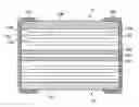
FIG. 1 is a cross-sectional view through one known stacked capacitor, of which there are many variants. The capacitor is formed of a plurality of capacitive layers 2a, 2b, etc., formed between respective electrode pairs of opposing polarities. For example, the layer 2a lies between electrodes 3a, 3b, and the layer 2b lies between electrodes 3b, 3c, etc. In the illustrated structure, alternate electrodes are secured to respective end caps 5a, 5b. The overall depth of the capacitor is denoted d, and the thickness of each layer is denoted df. Where the combined thicknesses of the capacitive layers do not make up the full depth of the capacitor, bulk layers (illustrated as 2e and 2f) can be provided. The overall depth of the capacitor may for example be determined by a required external package size.
The capacitive layers are formed of a dielectric material, such as a ceramic, while the electrodes themselves can be formed of a suitable precious or base metal. The terminating caps 5a, 5b can be of electroplated silver, electroplated copper, Pd/Ag or any suitable material.
There is an ongoing need to obtain the maximum possible capacitance of a stack capacitor structure of this type, at a maximum working voltage in a small as possible package size. Capacitance can be increased by increasing the electrode count (number of electrodes, 3a, 3b, etc), and/or increasing the spacing between electrodes (the layers thickness df to increase working voltage. There is however a trade-off between a maximum capacitive value achieved by a part, and the maximum working voltage. For example, at present, a structure of this type capable of operating at a voltage of 500V would deliver a maximum capacitance of about 0.5 μF. Conversely, parts of the capacitance value of 1 μF currently cannot exceed working voltages of around 200V. Moreover, it is important that capacitors are reliable, in that they should not fail over their intended lifetimes.
The inventors have devised a capacitive structure and a technique for forming the capacitive structure which allows these parameters to be modified, such that a part can deliver a higher capacitance at a higher working voltage, without significant failure rates.
According to an aspect of the present invention, there is provided a capacitive structure comprising: first and second components, at least one component comprising a plurality of capacitive layers of a dielectric, each layer arranged between electrodes of different polarity, wherein the first and second components are arranged in a stack separated by a stress reducing layer having a supporting structure with an open mesh in which air acts to reduce the transmissibility of cracks through the stress reducing layer.
In the following described embodiments, both of the first and second components have the structure of a plurality of layers of a dielectric, each layer arranged between electrodes of different polarity. Thus a capacitive part is formed. However, it is also possible to provide other electrical components in the stack, in place of a second capacitive component—for example, the component could be a varistor or inductive component. A still further possibility is that first and second components are a varistor or inductive component.
Still further possibilities include combining two different capacitor materials such as a low and high dielectric constant material or materials with differing properties with respect to operating parameters such as temperature.
Another aspect of the invention provides a method of making a capacitive structure comprising:
-
- forming a first component comprising a plurality of capacitive layers of a dielectric, each layer arranged between electrodes of differing pluralities;
- forming a second electrical component:
- providing a stress reducing layer between the first and second components to form a stack, the stress reducing layer having a supporting structure with an open mesh in which air acts to reduce the transmissibility of cracks through the stress reducing layer.
The stress reducing layer could be formed in a number of different ways, and according to the preferred embodiment which is described herein it is formed by forming a blended layer of an organic material, preferably particulate and a dielectric material between the first and second components, and sintering the structure so as to remove the organic particulate material, thereby leaving the open mesh.
When seeking to achieve the objective of the invention, that is to provide a part which can deliver a higher capacitance at a higher working voltage, the inventors had to contend with failures of the parts. For small chips and large, low voltage chips, product reliability is determined by material performance and manufacturing defect levels. The inventors have recognised that as chip size and working voltage increases, piezoelectric/electrostrictive stress cracking becomes important as an additional failure mechanism. In fact, the inventors have determined through repeated observation and analysis that piezoelectric/electrostrictive stress cracking eventually dominates the failure mechanism for large, higher voltage parts.
The stress reducing layer with an open mesh (a sponge-like structure) has been found to significantly reduce the effect of failures by cracking. This has permitted the construction of a part with a maximum working voltage of 500V and a capacitive value of 1 μF in a chip referred to as 2220 which has dimensions of 0.22″ (5.6 mm)×0.20″ (5.1 mm) and which has hitherto not been possible with these types of capacitive structures.
A principle advantage of the present invention is that for any given working voltage a higher capacitance per unit volume can be achieved than has been the case before. The invention has a wide applicability over all voltages and capacitance values, for example, from around 200V (or even lower) up to possible working voltages of 6 KV (or even higher). It is expected that the benefit of the invention can be achieved through capacitance values over a wide range from a few pF to μFr.
The method of making the capacitive structure in accordance with the invention fits in very well with existing manufacturing techniques where capacitive layers are screen printed. Once the correct amount of ceramic layers have been put down, with the intervening electrodes for the first component, the blended layer can be formed over these layers, following by subsequent layers for the other component. The entire structure can then be fired or sintered in a single step, simultaneously sintering the dielectric material of the capacitive layers and “burning off” the particulate organic material to leave the open mesh or sponge structure.
In this technique, carbon is particularly effective as the organic particulate material although it is expected that other materials (such as corn flour) would achieve the same result.
It will also be apparent that there are other ways of achieving the required spongy structure, for example, by using a coarser version of the ceramic material which would not bond together well after sintering, thereby offering the same advantage of a weaker structure allowing absorption of electrical stress. Furthermore, it may not be necessary when a blended layer is used for the organic material to be particulate—a binder blend could achieve a similar effect.
One example of a capacitive structure with which the techniques of the present invention can be used is that shown in FIG. 1. However, the technique can be applied to a wide range of layered capacitive structures, for example, using sectional or floating electrode patterns.
Moreover, the number of components in the part need not be restricted to two. It is possible to have more than two components, each separated from its adjacent component by an open mesh layer. This allows the thickness of each component to be reduced, thereby taking maximum advantage of properties of thinner “chips”.
The capacitance value and maximum working voltage of the part is affected by a number of different parameters, including the following:
-
- the number of electrodes, which is any suitable number but can typically lie between 20 and 100 and can extend up to 300;
- the thickness of an inner bulk layer which can be provided to separate the components on either side of the open mesh layer—this could have a value for example, between 65 and 200 microns, and more preferably between 70 and 150 microns (these values are the fired values—the corresponding green value for 65μ fired is 900;
- the thickness of open mesh layer itself, which can lie for example, between 10 and 200 microns, for example between 10 and 80 μm—values greater than 40 μm have been found to be preferred; and
- the thickness of the individual capacitive layers which can lie, for example, between 10 microns and 100 microns and can extend up to 200 μm. In one example, it lies between 30 microns and 40 microns.
(The above thicknesses are particularly appropriate for the 500 v/1 μF part).
The overall dimensions of the part can also play a part. Test parts which have been shown to deliver 1 μF at 500V have had a width of 5 mm, a length of 5.7 mm and thickness of 2.6 mm or 3.2 mm. It is expected that parts with dimensions in the following ranges would also be effective:
-
- Length between 3.2 mm and 20.5 mm or between 2 and 25 mm;
- Width between 1.6 mm and 15.5 mm or between 1 and 20 mm; and
- depth between 1.6 mm and 4 mm, or up to a maximum of at least 5 mm.
For a better understanding of the present invention and to show how the same may be carried into effect, reference will now be made by way of example, to the accompanying drawings in which:
FIG. 1 illustrates a section through a known capacitive structure;
FIG. 2 illustrates a section through a structure in accordance with one embodiment of the present invention;
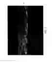
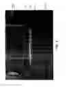
FIGS. 3 and 4 are SEM images showing the open mesh layer in two different magnifications;
FIG. 5 is a schematic diagram of the external configuration of a capacitive part;
FIG. 6 is a graph showing data for designing a capacitor;
FIGS. 7 and 8 are alternate sectional capacitor designs.
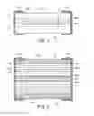
FIG. 2 illustrates a capacitive structure in accordance with one embodiment of the invention. The capacitor comprises ceramic capacitive layers 12a, 12b, etc., formed between pairs of electrodes 13a, 13b, 13c, etc. In this respect, the structure is somewhat similar to the structure shown in FIG. 1, and the principles of operation as a capacitor are the same. Of significant difference however is the fact that the capacitive structure of FIG. 2 comprises upper and lower components 14, 16, separated by a dividing layer 18. The upper and lower parts 14, 16 are held in a common capacitive structure by end caps 15a, 15b, formed for example, of electroplated silver. If necessary, to make up the required depth of the capacitor, outer bulk layers 12e, 12f can be provided. Each component can also have an inner bulk layer 12g, 12h adjacent the dividing layer 18. The dividing layer 18 performs two important functions. It has sufficient physical structure to hold together the upper and lower parts, but also is sufficiently loose grained that it can trap a sufficient quantity of air to prevent cracks being transmitted and causing failure. This is described in more detail in the following, but it has been determined that a layer with a sponge construction is the most effective. FIG. 3 is an SEM of the sponge layer itself, showing how it differs from the ceramic layer on either side of it. FIG. 4 is a lower scale SEM which shows the sponge layer 18 and also illustrates the ceramic layers 12a, 12b and electrodes 13a, 13b, etc.
Although the precise mechanism for reducing failure due to piezoelectric/electrostrictive cracks is not completely certain, it appears that stress is absorbed by the spongy layer 18 so that piezoelectric stress cracks do not form through the structure such as to cause failure.
Thus, the capacitive structure can withstand significantly higher voltages and deliver a higher capacitive value, without failure, than has hitherto been possible. In particular, a 500V, 1 μF capacitor is now enabled in a single package, of 2220 chip size.
According to one method of manufacture, the capacitive structure is formed as a sequence of layers. That is, a first layer of ceramic is put down onto a base substrate (which might involve a number of layering steps by screen printing, for example), allowed to dry, an electrode layer is formed, followed by a subsequent ceramic layer, etc. When sufficient ceramic and electrode layers have been put down to form the lower component 16 of a capacitor structure, a blended layer is put down which comprises, in one embodiment, a blend of carbon and the base ceramic material. The upper component of the capacitive structure can then be formed in a similar manner to the lower component. In a sintering step which dries the layers, the carbon is burnt off leaving a weakened ceramic “spongy” layer 18.
The resulting piece can then be cut into capacitive parts of the required dimensions.
The success of the above structure and technique in delivering a high voltage, high capacitance value structure which is resistant to failures is counterintuitive in that it provides a weaker layer at the centre of the capacitive structure. Nevertheless, the findings are impressive as set out in more detail later.
In seeking to develop a high voltage high capacitive failure-resistant structure, the inventors developed a useful understanding of piezoelectric/electrostrictive stress cracks which are formed when a high voltage is applied to a susceptible ceramic capacitor. The ceramic material is put under stress by the application of high voltage and a characteristic crack is formed, generally through the centre of the component. If the cracked component continues to be used with applied voltage, then an electrical failure will result, where the crack crosses opposing electrodes. This results in a short circuit condition arising as metal from the electrodes, for example, migrates through the crack and thereby allows an electrical short circuit.
If a part is susceptible to piezoelectric/electrostrictive cracking, then the crack can be generated at any stage of component use, i.e. at initial switch on, or during subsequent switching operations. Consequently, cracked components may not be detected at equipment test stage, but only later as field failures. Similarly, susceptible batches may be tested several times, generating widely different results, as crack formation is not always reproducible. It is thus a frustrating and hard to handle failure mechanism.
Prior to development of the present invention, the effect of piezoelectric/electrostrictive cracking as a failure mechanism was not sufficiently well understood to be incorporated into the normal design rules for designing multilayer ceramic capacitors. These rules sought to apply a minimum layer thickness between electrodes, expressed in volts per micron. This rule was thought to be applicable to a wide range of chip sizes and voltages, and generally speaking parts with higher capacitance values and lower working voltages could be manufactured by increasing the chip thickness to accommodate the increased specification. Chip thickness could be increased by increasing the thickness df of the capacitive layers, increasing the number of electrodes (and thus the number of layers), or increasing the depth of the bulk layers.
It should also be understood that in addition to considering these rules, there are practical limitations imposed by the manufacture of capacitors, either by manufacturing techniques or by cost implications. For example, there is a maximum chip size that can sensibly be automatically manufactured. Attempts by the applicant to manufacture a 500V 1 μF capacitor within that maximum 2220 chip size, using the conventional V/u rules resulted in a part that failed due to piezoelectric/electrostrictive cracking.
Attempts were made to increase the thickness of the ceramic layers (df), in line with what was considered standard practice to reduce the V/u rating. The inventors noticed however that parts re-made with thicker layers still suffered from similar failure levels due to piezoelectric/electrostrictive cracking. Further increases in layer thicknesses offered no improvement.
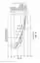
Following analysis, the inventors determined that failures due to piezoelectric/electrostrictive cracking were related to chip dimensions. Consider FIG. 5, which shows a capacitor having a depth d, with w and length l. The inventors determined that large, thicker chips (large l, large w, large d) were significantly more prone to failure than small thinner chips (small w, l, and d), or even large thinner chips (large w, l; small d). The inventors also noticed that the thicker the layer between electrodes (df) the more likely it was to induce piezoelectric/electrostrictive cracking.
Thus, the conventional rules would not permit the construction of a capacitive structure for large capacitance, high voltage components which were not prone to failure by cracking.
FIG. 6 illustrates a graph of maximum volts per micron (V/u) versus chip thickness in millimetres for a “2220” chip. As shown in the right-hand side of the graph, different geometrical icons represent different layer thicknesses. In order to form different overall chip thicknesses (as on the X scale of the graph), the number of electrodes, and thus the number of layers was adjusted.
Consider the data for a layer thickness between 30-40 microns, at a chip thickness of around 2.7 mm. At this point, the maximum volt per micron is around 12 using conventional design rules. Similarly, consider a structure with a layer thickness of between 30-40 microns, and a chip thickness of around 3.4 mm. The maximum volt per micron is around 11.
Consider now the two points marked with a star, labelled “TP1” (Test Part 1) and “TP2” (Test Part 2). Note that the maximum volts per micron for TP1 are around 17-18 (significantly higher than its conventional counterpart). The maximum volt per micron for TP2 is around 14, significantly greater than 12. In both cases, the part performs more like chips at least one millimetre thinner according to the conventional design strategy. More specific information on the test parts is given in the following.
The test parts (2 batches TP1/TP2) had the following construction based on fired measurements:
-
- a) Ceramic layers 210/250 microns
- b) 34 electrode and ceramic layers of 31/37 microns
- c) Ceramic layers of 62/74 microns
- d) 12 sponge layer prints (approx 50 microns)
- e) Ceramic layers of 62/74 microns
- f) 34 electrode and ceramic layers of 31/37 microns
- g) Ceramic layers 210/250 microns
1. Dimensions of Chip
| Length | Width | Thickness | |
| Experimental parts TP1/TP2 | 5.7 mm | 5.0 mm | 2.6 mm/3.2 mm |
2. Thickness of Each Layer;
-
- Experimental parts “green layer” (ceramic prior to sintering) thickness 37.5 and 44.5 microns, equates to fired layers of 31 and 37 microns approx.
3. Overall Thickness of Chip as Above;
-
- thickness of each stacked component of the finished chip was 1.3 mm (TP1) and 1.6 mm (TP2).
4. Materials;
-
- The base ceramic (dielectric) material has BaTiO3 as the primary ingredient, and is classified as an X7R material.
- The sponge layer 18 as present in the finished product is also made entirely of the base ceramic material (BaTiO3 for test parts). The layer was made into a sponge by mixing the ceramic ink with carbon which after sintering formed the spongy layer 18.
5. Blend Percentages
-
- The ceramic sponge ink was made by blending 60% of our black coverplate ink (9.6% carbon) with 40% BaTiO3 based dielectric ink (65% solids).
- This gave an ink containing weight percentages 26% BaTiO3 based dielectric, 5.8% carbon, 68.2% organic solvents plus binders.
The manufacturing process described above is a screen printing process.
A tape process would also be capable of producing the proposed parts. The tape process involves more stages to replace the screen printing stage, but other than this, the manufacturing processes are essentially the same.
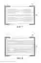
FIG. 7 shows an alternate capacitor design in section. In FIG. 7, each component of the design has two sections, although 4, 6, 8, 10 and more sections are also possible. Sectional or floating electrode patterns are used for higher voltages, allowing voltage to be dropped across each section. There are many variants; according to one prior art variant, a two section screen at rated voltage 1 kV would have 500V across each section. A four section screen at 4 kV would have 1 kV across each section, etc.
FIG. 8 shows a fractional capacitor design which is commonly used at mid voltages to reduce surface flashover.
It will be appreciated that while certain embodiments of the invention have been described, there is no intention to limit the invention to these embodiments as many variants are possible. In particular, although the 500V/1 μF/2220 part has been a part which has been particularly elusive in the industry, is readily apparent that the principles of the invention may be applied to parts of different working voltages, different capacitive values and of different dimensions. It is anticipated that the principles described herein will be widely applicable to improve the delivery of many different capacitive structures. For example, the following table gives a range of different parts to which the technique described herein can be applied.
| TABLE I |
| Maximum capacitance values |
| Voltage | 1812 | 2220 | 3640 | 5550 | 8060 |
| 100 | Vdc | — | — | — | 22 | uF | 33 | uF |
| 200/250 | Vdc | 1.0 | uF | 2.2 | uF | 5.6 | uF | 10 | uF | 15 | uF |
| 500 | Vdc | 470 | nF | 1.2 | uF | 2.7 | uF | 3.9 | uF | 6.8 | uF |
| 630 | Vdc | 330 | nF | 1.0 | uF | 2.2 | uF | 3.3 | uF | 3.9 | uF |
| 1 | kVdc | 180 | nF | 470 | nF | 1.0 | uF | 1.2 | uF | 1.8 | uF |
| 1.2 | kVdc | 100 | nF | 220 | nF | 470 | nF | 820 | nF | 1.2 | uF |
| 1.5 | kVdc | 56 | nF | 150 | nF | 330 | nF | 560 | nF | 680 | nF |
| 2 | kVdc | N/a | 100 | nF | 150 | nF | 270 | nF | 470 | nF |
| 2.5 | kVdc | — | — | — | 150 | nF | 270 | nF |
| 3 | kVdc | — | — | — | 100 | nF | 220 | nF |
| 4 | kVdc | — | — | — | 68 | nF | 100 | nF |
Furthermore, it is anticipated that the principles of the invention can be applied in a scenario where the first and second components are of different base ceramic materials having therefore different properties. Thus, it would be possible to produce a capacitive structure in which a first component had particularly good temperature resistant properties in one range, combined with a second component having particularly good temperature resistant properties in another range. In this way it would be possible to “blend” the characteristics of different ceramics to achieve a capacitive structure capable of operating over a wider range of variables than is presently possible.
In another variant, a lead is soldered to each termination of the capacitive structure. The structure can then be coated with a conformal coating to protect against environment/voltage.
Furthermore, although the above discussion has focused on the capacitive structure, it is expected that the techniques discussed herein could be usefully extended to varistor and/or inductor structures.
Claims
1. A capacitive structure comprising: first and second components, at least one component comprising a plurality of capacitive layers of a dielectric, each layer arranged between electrodes of different polarity, wherein the first and second components are arranged in a stack separated by a stress reducing layer having a supporting structure with an open mesh in which air acts to reduce the transmissibility of cracks through the stress reducing layer.
2. A capacitive structure according to claim 1, comprising terminating caps at opposed ends of the stack, each cap extending the full depth of the stack, wherein at least some of the electrodes contact one of the terminating caps and at least some others of the electrodes contact the other of the terminating caps.
3. A capacitive structure according to claim 1, wherein the supporting structure is formed of a ceramic material.
4. A capacitive structure according to claim 3, wherein the dielectric layer is a ceramic material.
5. A capacitive structure according to claim 1, wherein the ceramic material of the supporting structure is formed of a ceramic material which is the same as a ceramic material of the dielectric.
6. A capacitive structure according to claim 5, wherein the ceramic material is an X7R dielectric material.
7. A capacitive structure according to claim 5, having a depth of between 1.6 mm and 4 mm.
8. (canceled)
9. (canceled)
10. A capacitive structure according to claim 1, wherein the first and second components have the same depth.
11. (canceled)
12. A capacitive structure according to claim 1, wherein each capacitive layer has a thickness of between 10 μm and 100 μm.
13. (canceled)
14. A capacitive structure according to claim 1, which has a maximum voltage of 500V and a capacitive value of 1 μF.
15. A capacitive structure according to claim 14, having a width between 3.2 mm and 20.5 mm, and a length between 1.6 mm and 15.5 mm.
16. A capacitive structure according to claim 1, wherein each component has a bulk dielectric layer forming an outer layer of the component.
17. (canceled)
18. A capacitive structure according to claim 16, wherein each component has an inner bulk layer adjacent the stress reducing layer.
19. (canceled)
20. (canceled)
21. A capacitive structure according to claim 1, wherein both of the first and second components comprise a plurality of capacitive layers of dielectric, each layer arranged between electrodes of different polarity, whereby the capacitive structure forms a capacitor.
22. A capacitive structure according to claim 1, wherein the first component comprises a plurality of capacitive layers of a dielectric, each layer arranged between electrodes of different polarity, and wherein the second component has a varistor or inductive characteristic.
23. A capacitive structure according to claim 1, comprising at least one further component, separated from an adjacent one of the first and second components by a further stress reducing layer.
24. A method of making a capacitive structure comprising:
forming a first component comprising a plurality of capacitive layers of a dielectric, each layer arranged between electrodes of differing polarities;
forming a second electrical component:
providing a stress reducing layer between the first and second components to form a stack, the stress reducing layer having a supporting structure with an open mesh in which air acts to reduce the transmissibility of cracks through the stress reducing layer.
25. A method according to claim 24, wherein the second component comprises a plurality of capacitive layers of a dielectric, each layer arranged between electrodes of different polarities.
26. A method according to claim 24, wherein the step of providing the stress reducing layer comprises forming a blended layer of an organic particulate material and a dielectric material between the first and second components and sintering the structure so as to remove the organic material thereby leaving the open mesh.
27. (canceled)
28. A method according to claim 26, wherein the organic particulate material comprises carbon.
29. (canceled)
30. (canceled)
31. A method according to claim 24, wherein each of the plurality of capacitive layers is formed by screen printing a layer of ceramic ink and allowing to dry before a subsequent capacitive layer is formed.
32. A method according to claim 24, wherein the first and second components are formed in a tape process.
33. A layered structure comprising: first and second components, at least one component comprising a plurality of layers of a dielectric, each layer arranged between electrodes, wherein the first and second components are arranged in a stack separated by a stress reducing layer having a supporting structure with an open mesh in which air acts to reduce the transmissability of cracks through the stress reducing layer.
34. A layered structure according to claim 33 wherein each of the first and second components is selected from a capacitive component, a varistor component and an inductive component.
Images & Drawings included:

Sources:
- United States Patent and Trademark Office - verify current appl. status at the USPTO↗
Similar patent applications:
- » 20190033357
Capacitive structure and method for determining an amount of charge using the capacitive structure - » 15337026
MOS capacitive structure of reduced capacitance variability - » 11372830
Method of forming a metal interconnect with capacitive structures that adjust the capacitance of the interconnect - » 10010696
Multilevel metal interconnect and method of forming the interconnect with capacitive structures that adjust the capacitance of the interconnect - » 20170053989
TERMINATION STRUCTURE WITH MULTIPLE EMBEDDED POTENTIAL SPREADING CAPACITIVE STRUCTURES FOR TRENCH MOSFET - » 20150214312
Termination structure with multiple embedded potential spreading capacitive structures for trench MOSFET - » 20110198605
Termination structure with multiple embedded potential spreading capacitive structures for trench MOSFET and method - » 20180090558
Capacitive structure in a semiconductor device having reduced capacitance variability - » 20190349687
MEMS structure, capacitive sensor, piezoelectric sensor, acoustic sensor having mems structure - » 20210143673
Capacitive coupler structure and wireless power transfer system including the capacitive coupler structure
Recent applications in this class:
- » 20250069804 2025-02-27
MULTILAYER ELECTRONIC COMPONENT - » 20220028610 2022-01-27
Method for producing resin mold-type electronic component and resin mold-type electronic component - » 20210313112 2021-10-07
Capacitor - » 20200357572 2020-11-12
Transformer for vacuum capacitor type instrument - » 20200350121 2020-11-05
Film capacitor manufacturing method and case - » 20200279690 2020-09-03
Capacitor - » 20200227207 2020-07-16
Ceramic package - » 20180182546 2018-06-28
CAPACITOR UNIT AND ELECTRICAL APPARATUS - » 20160093435 2016-03-31
Terminal bushing sealing element - » 20150325368 2015-11-12
Thin film capacitor
Recent applications for this Assignee:
- » 20220020532 2022-01-20
Electrical component having layered structure with improved breakdown performance - » 20170069427 2017-03-09
Dielectric material and capacitor comprising the dielectric material