Semiconductor structure including stacked structure and method for forming the same
US20150187694A1
2015-07-02
14/143,040
2013-12-30
✅ Patent granted
US 9,293,348 B2
2016-03-22
-
-
Alexander Oscar Williams
McClure, Qualey & Rodack, LLP
2033-12-30
Abstract:
A semiconductor structure and a method for forming the same are provided. The semiconductor structure includes a substrate, a stacked structure, a dielectric layer, a conductive structure, a dielectric structure and a conductive plug. The stacked structure includes dielectric films and conductive films arranged alternately. The dielectric layer is between the conductive structure and a sidewall of the stacked structure. The dielectric structure is on the stacked structure and defining a through via. The conductive plug fills the through via and physically contacts one of the conductive films exposed by the through via and adjoined with the dielectric layer.
Inventors:
- Yen-Hao Shih 19 🇹🇼 New Taipei City, Taiwan
- Erh-Kun Lai 56 🇹🇼 Taichung City, Taiwan
- Guan-Ru Lee 12 🇹🇼 Kaohsiung City, Taiwan
- Erh-Kun Lai 78 🇹🇼 Taichung, Taiwan
- Yen-Hao Shih 21 🇹🇼 New Taipei, Taiwan
- Guan-Ru Lee 11 🇹🇼 Kaohsiung, Taiwan
Assignee:
- MACRONIX INTERNATIONAL CO., LTD. 2,995 🇹🇼 Hsinchu, Taiwan
Applicant:
Interested in similar patents?
Get notified when new applications in this technology area are published.
Classification:
H01L23/5226 » CPC further
Details of semiconductor or other solid state devices; Arrangements for conducting electric current within the device in operation from one component to another, i.e. interconnections, e.g. wires, lead frames including external interconnections consisting of a multilayer structure of conductive and insulating layers inseparably formed on the semiconductor body Via connections in a multilevel interconnection structure
H01L23/53271 » CPC further
Details of semiconductor or other solid state devices; Arrangements for conducting electric current within the device in operation from one component to another, i.e. interconnections, e.g. wires, lead frames including external interconnections consisting of a multilayer structure of conductive and insulating layers inseparably formed on the semiconductor body characterised by the materials; Conductive materials containing semiconductor material, e.g. polysilicon
H01L27/1052 » CPC further
Devices consisting of a plurality of semiconductor or other solid-state components formed in or on a common substrate including semiconductor components specially adapted for rectifying, oscillating, amplifying or switching and having at least one potential-jump barrier or surface barrier; including integrated passive circuit elements with at least one potential-jump barrier or surface barrier the substrate being a semiconductor body including a plurality of individual components in a repetitive configuration including field-effect components Memory structures and multistep manufacturing processes therefor not provided for in groups -
H01L23/532 IPC
Details of semiconductor or other solid state devices; Arrangements for conducting electric current within the device in operation from one component to another, i.e. interconnections, e.g. wires, lead frames including external interconnections consisting of a multilayer structure of conductive and insulating layers inseparably formed on the semiconductor body characterised by the materials
H01L21/76805 » CPC further
Processes or apparatus adapted for the manufacture or treatment of semiconductor or solid state devices or of parts thereof; Manufacture or treatment of devices consisting of a plurality of solid state components formed in or on a common substrate or of parts thereof; Manufacture of integrated circuit devices or of parts thereof; Manufacture of specific parts of devices defined in group; Applying interconnections to be used for carrying current between separate components within a device comprising conductors and dielectrics characterised by the formation and the after-treatment of the dielectrics, e.g. smoothing by forming openings in dielectrics the opening being a via or contact hole penetrating the underlying conductor
H01L21/76877 » CPC further
Processes or apparatus adapted for the manufacture or treatment of semiconductor or solid state devices or of parts thereof; Manufacture or treatment of devices consisting of a plurality of solid state components formed in or on a common substrate or of parts thereof; Manufacture of integrated circuit devices or of parts thereof; Manufacture of specific parts of devices defined in group; Applying interconnections to be used for carrying current between separate components within a device comprising conductors and dielectrics characterised by the formation and the after-treatment of the conductors Filling of holes, grooves or trenches, e.g. vias, with conductive material
H01L21/76883 » CPC further
Processes or apparatus adapted for the manufacture or treatment of semiconductor or solid state devices or of parts thereof; Manufacture or treatment of devices consisting of a plurality of solid state components formed in or on a common substrate or of parts thereof; Manufacture of integrated circuit devices or of parts thereof; Manufacture of specific parts of devices defined in group; Applying interconnections to be used for carrying current between separate components within a device comprising conductors and dielectrics characterised by the formation and the after-treatment of the conductors; Filling of holes, grooves or trenches, e.g. vias, with conductive material Post-treatment or after-treatment of the conductive material
H01L21/768 IPC
Processes or apparatus adapted for the manufacture or treatment of semiconductor or solid state devices or of parts thereof; Manufacture or treatment of devices consisting of a plurality of solid state components formed in or on a common substrate or of parts thereof; Manufacture of integrated circuit devices or of parts thereof; Manufacture of specific parts of devices defined in group Applying interconnections to be used for carrying current between separate components within a device comprising conductors and dielectrics
H01L21/76834 » CPC further
Processes or apparatus adapted for the manufacture or treatment of semiconductor or solid state devices or of parts thereof; Manufacture or treatment of devices consisting of a plurality of solid state components formed in or on a common substrate or of parts thereof; Manufacture of integrated circuit devices or of parts thereof; Manufacture of specific parts of devices defined in group; Applying interconnections to be used for carrying current between separate components within a device comprising conductors and dielectrics characterised by the formation and the after-treatment of the dielectrics, e.g. smoothing characterised by the formation of thin functional dielectric layers, e.g. dielectric etch-stop, barrier, capping or liner layers formation of thin insulating films on the sidewalls or on top of conductors
H01L29/792 » CPC further
Semiconductor devices adapted for rectifying, amplifying, oscillating or switching, or capacitors or resistors with at least one potential-jump barrier or surface barrier, e.g. PN junction depletion layer or carrier concentration layer; Details of semiconductor bodies or of electrodes thereof; Multistep manufacturing processes therefor; Types of semiconductor device ; Multistep manufacturing processes therefor controllable by only the electric current supplied, or only the electric potential applied, to an electrode which does not carry the current to be rectified, amplified or switched; Unipolar devices, e.g. field effect transistors; Field effect transistors with field effect produced by an insulated gate with charge trapping gate insulator, e.g. MNOS-memory transistors
H01L23/528 » CPC main
Details of semiconductor or other solid state devices; Arrangements for conducting electric current within the device in operation from one component to another, i.e. interconnections, e.g. wires, lead frames including external interconnections consisting of a multilayer structure of conductive and insulating layers inseparably formed on the semiconductor body layout of the interconnection structure
H01L27/105 IPC
Devices consisting of a plurality of semiconductor or other solid-state components formed in or on a common substrate including semiconductor components specially adapted for rectifying, oscillating, amplifying or switching and having at least one potential-jump barrier or surface barrier; including integrated passive circuit elements with at least one potential-jump barrier or surface barrier the substrate being a semiconductor body including a plurality of individual components in a repetitive configuration including field-effect components
H01L23/522 IPC
Details of semiconductor or other solid state devices; Arrangements for conducting electric current within the device in operation from one component to another, i.e. interconnections, e.g. wires, lead frames including external interconnections consisting of a multilayer structure of conductive and insulating layers inseparably formed on the semiconductor body
H01L21/3205 IPC
Processes or apparatus adapted for the manufacture or treatment of semiconductor or solid state devices or of parts thereof; Manufacture or treatment of semiconductor devices or of parts thereof the devices having at least one potential-jump barrier or surface barrier, e.g. PN junction, depletion layer or carrier concentration layer the devices having semiconductor bodies comprising elements of Group IV of the Periodic System or AB compounds with or without impurities, e.g. doping materials; Treatment of semiconductor bodies using processes or apparatus not provided for in groups - to form insulating layers thereon, e.g. for masking or by using photolithographic techniques ; After treatment of these layers; Selection of materials for these layers Deposition of non-insulating-, e.g. conductive- or resistive-, layers on insulating layers; After-treatment of these layers
H01L27/115 IPC
Devices consisting of a plurality of semiconductor or other solid-state components formed in or on a common substrate including semiconductor components specially adapted for rectifying, oscillating, amplifying or switching and having at least one potential-jump barrier or surface barrier; including integrated passive circuit elements with at least one potential-jump barrier or surface barrier the substrate being a semiconductor body including a plurality of individual components in a repetitive configuration including field-effect components; Read-only memory structures [ROM] and multistep manufacturing processes therefor Electrically programmable read-only memories; Multistep manufacturing processes therefor
H01L29/423 IPC
Semiconductor devices adapted for rectifying, amplifying, oscillating or switching, or capacitors or resistors with at least one potential-jump barrier or surface barrier, e.g. PN junction depletion layer or carrier concentration layer; Details of semiconductor bodies or of electrodes thereof; Multistep manufacturing processes therefor; Electrodes ; Multistep manufacturing processes therefor characterised by their shape, relative sizes or dispositions not carrying the current to be rectified, amplified or switched
H01L29/66 IPC
Semiconductor devices adapted for rectifying, amplifying, oscillating or switching, or capacitors or resistors with at least one potential-jump barrier or surface barrier, e.g. PN junction depletion layer or carrier concentration layer; Details of semiconductor bodies or of electrodes thereof; Multistep manufacturing processes therefor Types of semiconductor device ; Multistep manufacturing processes therefor
Description
BACKGROUND
1. Technical Field
The invention relates to a semiconductor structure and a method for forming the same and more specifically to a contact pad structure and a method for forming the same.
2. Description of the Related Art
The demand of memory devices increases complying with a growth in market of the electronic products. There are several types of memory devices, such as volatile and non-volatile memory (NVM) devices.
The dynamic random access memory (DRAM) and the cache memory are volatile memories. Although a read access velocity of a volatile memory is fast, a non-volatile memory can be used as a hard disk since data stored in non-volatile memories will exist even when the current pinch off. According to read/write characteristic differences of memory devices, the non-volatile memory can be separated into read only memory (ROM) and flash memory. Recently, flash memory has been widely used in a variety of filed, such as cell phone, digital camera and MP3.
In order to increase a storage capacity of the memory in a limited memory volume, a three dimensional (3D) memory is developed. In a 3D memory, pitches between each of elements are smaller and an element density in an unit area of the 3D memory is larger.
SUMMARY
According to one embodiment, a semiconductor structure is provided. The semiconductor structure comprises a substrate, a stacked structure, a dielectric layer, a conductive structure, a dielectric structure and a conductive plug. The stacked structure comprises dielectric films and conductive films arranged alternately. The dielectric layer is between the conductive structure and a sidewall of the stacked structure. The dielectric structure is on the stacked structure and defining a through via. The conductive plug fills the through via and physically contacts one of the conductive films exposed by the through via and adjoined with the dielectric layer.
According to another embodiment, a method for forming a semiconductor structure is provided. The method comprises following steps. A stacked structure comprising dielectric films and conductive films arranged alternately is formed on a substrate. A dielectric layer is formed on a sidewall of the stacked structure. A conductive structure is formed on the dielectric layer. A dielectric structure is formed on the stacked structure. A conductive plug is formed to pass through the dielectric structure and physically contact one portion of one of the conductive films having an electric conductivity higher than an electric conductivity of the other portion of the one of the conductive films.
BRIEF DESCRIPTION OF THE DRAWINGS
FIGS. 1A˜6C illustrate a method for forming a semiconductor structure.
DETAILED DESCRIPTION
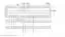
FIGS. 1A˜6C illustrate a method for forming a semiconductor structure. The figures marked with “A” are top views, and the figures marked with “B” are cross-section views taken along BB line in the top views.
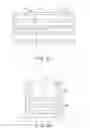
Referring to FIGS. 1A and 1B, a stacked structure 102 is formed on a substrate 104, The stacked structure 102 comprises dielectric films 106 and a conductive film 108 comprising conductive films 108A, 108B, 108C, 108D arranged alternately. Amount of the dielectric film and the conductive film may be varied according to actual demands properly.
In embodiments, the conductive films 108A, 108B, 108C, 108D comprise an un-doped Si or an un-doped polysilicon. The dielectric film 106 may comprise an oxide, a nitride, an oxynitride, such as silicon oxide, silicon nitride, silicon oxynitride, or other suitable materials. The conductive films 108A, 108B, 108C, 108D are conductively insulated from each other by the dielectric films 106. As shown in FIG. 1A, the stacked structure 102 comprise a pad portion 110 in a pad region 112 and strip portions 114 in an array region 116. An amount of the strip portions 114 extended from a side all of the pad portion 110 may be varied according to actual demands.
Referring to FIGS. 2A and 2B, a dielectric layer 118 is formed on an upper surface and a sidewall of the stacked structure 102. The dielectric layer 118 may comprise a conformal material formed by a deposition method such as a CVD method or a PVD method, or other suitable methods. The dielectric layer 118 may comprise an oxide, a nitride, an oxynitride, such as silicon oxide, silicon nitride, silicon oxynitride, or other suitable materials. In one embodiment, the dielectric layer 118 has a multi-layer structure such as an ONO structure or an ONONO structure, but is not limited thereto, and may have a single-layer structure, or other suitable structures. In one embodiment, the dielectric layer 118 is a multi-layer structure of tunneling layer/trapping layer/blocking layer.
A conductive structure 120 is formed on the dielectric layer 118 in the pad region 112. A word line (WL) 122 is formed on the dielectric layer 118, not shown in FIG. 2A, in the array region 116. In one embodiment, the conductive structure 120 and the word line 122 are formed at the same time. For example, the conductive structure 120 and the word line 122 may be formed by a process comprising forming a conductive material and patterning the conductive material by the same photolithography process. The photolithography process for forming the conductive structure 120 and the word line 122 at the same time can reduce etch loading effect, compared to a photolithography for forming only the word line 122. Therefore, an accuracy of feature of a product and a yield can be increased.
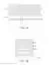
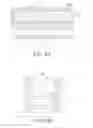
Referring to FIGS. 3A and 3B, for example, upper portions of conductive structure 120, the dielectric layer 118 (not shown in FIG. 3A) and the stacked structure 102 are removed to form an opening 124 exposing the conductive film 108. In embodiments, the opening 124 in different regions exposes the conductive films 108A, 108B, 108C, 108D of different levels. According to one embodiment, for example, the semiconductor structure may have a stair plane structure as shown in a cross-section view of FIG. 3C taken from a line corresponding a CC line in FIG. 3A. As shown in FIG. 3C, the opening 124 exposes the conductive film 108 of different levels.
Referring to FIGS. 4A and 4B, the opening 124 is filled with a dielectric structure 126. The dielectric structure 126 may comprise an oxide, a nitride, an oxynitride, such as silicon oxide, silicon nitride, silicon oxynitride, or other suitable materials. The dielectric structure 126 may be formed by a deposition method such as CVD method or PVD method, or other suitable methods. A portion of the dielectric structure 126 is removed to define a through via 128 exposing the conductive film 108B, for example. Based on the similar concepts, through via 128 in other regions exposes other conductive film such as conductive films 108A, 108C, 108D, not described in detail herein for the sake of brevity.
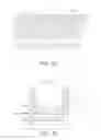
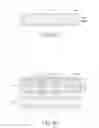
Referring to FIGS. 5A and 5B, and FIG. 5C which shows only the conductive film 108B and the dielectric layer 118, a portion of the conductive film 108B exposed by the through via 128 is removed until an etching condition reaches the dielectric layer 118. In one embodiment, the conductive film 108B is removed by an isotropic etching step having a high selectivity to the dielectric layer 118, i.e. mainly etching the conductive film 108B of un-doped Si or polysilicon. For example, the etching step comprises a wet etching of TMAH dip. In other embodiments, a chemical dry etching method may be used.
Referring to FIGS. 6A and 6B, and FIG. 6C which shows only the conductive film 108B and the dielectric layer 118, the removed portion 130 (FIGS. 5A˜5C) of the conductive film 108B and the through via 128 are filled with a conductive material to a (one) portion 132 of the conductive film 108B and a conductive plug 134 passing through the dielectric structure 126 and physically contacting the one portion 132 the conductive film 108B. The conductive material may comprise a doped Si or a doped polysilicon, such as a heavily doped (N+) polysilicon, or a metal containing material such as TiN (barrier layer), W, Cu, metal silicides, etc. For example, the doped polysilicon may be formed by an in-situ deposition method. The conductive material may be formed by any suitable method. The one portion 132 of the conductive film 108B and the conductive plug 134 may have the same material or different materials. For example, the one portion 132 may have the doped polysilicon, and the conductive plug 134 may have a structure of TiN barrier layer and a W fill. A CMP process may be performed to form an upper planer surface.
The conductive plug 134 is separated or conductively insulated from the other conductive films, for example conductive films 108A, 108C, by the dielectric structure 126 and the dielectric film 106.
In embodiments, the conductive material for forming the one portion 132 of the conductive film 108B is different the conductive material for forming the other portion 136 of the conductive film 108B separated from the conductive plug 134. In other words, the conductive film 108B has a material interface 138 of the different conductive materials. The material interface 138 is adjoined with (or physically contacts) the dielectric layer 118 (not shown in FIGS. 1A, 2A, 3A, 4A, for the sake of brevity).
In one embodiment, an electric conductivity of the one portion 132 is higher than an electric conductivity of the other portion 136 of the conductive film 108B comprising the material illustrated in FIGS. 1A and 1B. For example, the conductive material for the one portion 132 comprises a doped polysilicon, such as a heavily doped (N+) polysilicon, or a metal containing material such as W, Cu, TiN, etc., and the conductive material for the other portion 136 comprises an un-doped polysilicon.
The conductive films 108A, 108B, 108C, 108D (FIG. 1B) of the strip portions 114 of the stacked structure 102 in the array region 116 are functioned as bit lines (BL). In embodiments, the bit lines are formed by an un-doped polysilicon, which usually has higher resistance than a doped polysilicon, such as a heavily doped (N+) polysilicon, or a metal containing material such as W, Cu, TiN, etc., and therefore a normal state of the bit lines of a three-dimensional (3D) stacked NAND flash memory is in an “off” state (normally OFF) and the bit lines can be easily controlled to turn “on” by applying a proper voltage to a string select line (SSL) (not shown) between the pad region 112 and the array region 116.
A proper voltage (such as 3.3V) may be applied to the conductive structure 120 functioned as an assistant gate to generate an inversion layer in a portion of the conductive films 108A, 108B, 108C, 108D (FIG. 1B) adjoined to the dielectric layer 118. Since the one portion 132 of the conductive film 108B functioned as a BL pad is also adjoined to the dielectric layer 118, the formed inversion layer overlaps (or physically connects) with the one portion 132 of the conductive film. The inversion layer and the one portion 132 of the conductive film 108B form a current path of low resistance so as to increase contact efficiency (or electrical conductivity) for a contact structure comprising the conductive film 108B and the conductive plug 134.
While the invention has been described by way of example and in terms of the exemplary embodiment(s), it is to be understood that the invention is not limited thereto. On the contrary, it is intended to cover various modifications and similar arrangements and procedures, and the scope of the appended claims therefore should be accorded the broadest interpretation so as to encompass all such modifications and similar arrangements and procedures.
Claims
1. A semiconductor structure, comprising:
a substrate;
a stacked structure comprising dielectric films and conductive films arranged alternately;
a dielectric layer;
a conductive structure, the dielectric layer being between the conductive structure and a sidewall of the stacked structure;
a dielectric structure on the stacked structure and defining a through via; and
a conductive plug filling the through via and physically contacting one of the conductive films exposed by the through via and adjoined with the dielectric layer.
2. The semiconductor structure according to claim 1, wherein a material of one portion of the one of the conductive films physically contacting the conductive plug is different from a material of the other portion of the one of the conductive films separated from the conductive plug.
3. The semiconductor structure according to claim 1, wherein an electric conductivity of one portion of the one of the conductive films physically contacting the conductive plug is higher than an electric conductivity of the other portion of the one of the conductive films separated from the conductive plug.
4. The semiconductor structure according to claim 1, wherein a material of one portion of the one of the conductive films physically contacting the conductive plug comprises a doped poly silicon or a metal containing material, a material of the other portion of the one of the conductive films separated from the conductive plug comprises an un-doped polysilicon.
5. The semiconductor structure according to claim 1, wherein one portion of the one of the conductive films having a doped polysilicon material or a metal containing material physically contacts the dielectric layer.
6. The semiconductor structure according to claim 1, wherein the conductive plug is separated from the other of the conductive films by the dielectric structure and the dielectric layer.
7. The semiconductor structure according to claim 1, wherein an upper portion of the stacked structure above the one of the conductive films defines an opening filled with the dielectric structure.
8. The semiconductor structure according to claim 1, comprising a plurality of the conductive plugs respectively physically contacting the different conductive films.
9. The semiconductor structure according to claim 8, wherein one portion of each of the conductive films physically contacts the corresponding one of the conductive plugs.
10. The semiconductor structure according to claim 1, wherein each of the dielectric films has a material interface of different materials.
11. The semiconductor structure according to claim 10, wherein the material interface physically contacts the dielectric layer.
12. The semiconductor structure according to claim 11, comprising an array region and a pad region, the conductive plug is arranged in the pad region.
13. A method for forming a semiconductor structure, comprising:
forming a stacked structure comprising dielectric films and conductive films arranged alternately on a substrate;
forming a dielectric layer on a sidewall of the stacked structure;
forming a conductive structure on the dielectric layer;
forming a dielectric structure on the stacked structure; and
forming a conductive plug passing through the dielectric structure and physically contacting one portion of one of the conductive films having an electric conductivity higher than an electric conductivity of the other portion of the one of the conductive films.
14. The method for forming the semiconductor structure according to claim 13, comprising:
removing a portion of the one of the conductive films; and
filling the removed portion of the one of the conductive films with a conductive material to form the one of the conductive films having a material interface of materials having different electric conductivities.
15. The method for forming the semiconductor structure according to claim 13, comprising:
removing an upper portion of the stacked structure above the one of the conductive films to define an opening;
filling the opening with the dielectric structure;
removing a portion o the dielectric structure to define a through via exposing the one of the conductive films;
removing a portion of the one of the conductive film exposed by the through via; and
forming a conductive material to fill the removed portion of the one of the conductive film and the through via defined by the dielectric structure.
16. The method for forming the semiconductor structure according to claim 15, wherein the portion of the one of the conductive film exposed by the through via is removed by an isotropic etching step.
17. The method for forming the semiconductor structure according to claim 13, comprising:
forming a conductive material on the stacked structure in an array region and a pad region; and
patterning the conductive material to form a word line in the array region and the conductive structure in the pad region.
18. The method for forming the semiconductor structure according to claim 17, wherein the word line and the conductive structure are formed simultaneously.
19. The method for forming the semiconductor structure according to claim 13, comprising removing an upper portion of the dielectric layer and the conductive structure.
20. The method for forming the semiconductor structure according to claim 13, wherein the conductive films are separated from each other by the dielectric films.
Images & Drawings included:

Sources:
- United States Patent and Trademark Office - verify current appl. status at the USPTO↗
Similar patent applications:
Recent applications in this class:
- » 20250293154 2025-09-18
LAYOUT FOR REDUCING LOADING AT LINE SOCKETS AND/OR FOR INCREASING OVERLAY TOLERANCE WHILE CUTTING LINES - » 20250285967 2025-09-11
METAL-INSULATOR-METAL CAPACITOR AND METHODS OF MANUFACTURING - » 20250285966 2025-09-11
SEMICONDUCTOR STRUCTURE AND METHOD FOR FORMING THE SAME - » 20250285965 2025-09-11
PINWHEEL-SHAPED CONNECTIONS BETWEEN DIAGONALLY OPPOSITE INTEGRATED CIRCUITS IN A MULTI-CHIP MODULE TO REDUCE NUMBER OF ROUTING LAYERS - » 20250285964 2025-09-11
DEEP VIA STRUCTURES FOR STACKED TRANSISTOR DEVICES - » 20250279357 2025-09-04
SEMICONDUCTOR STORAGE DEVICE AND METHOD FOR MANUFACTURING SEMICONDUCTOR STORAGE DEVICE - » 20250273567 2025-08-28
SEMICONDUCTOR INTEGRATED CIRCUIT DEVICE - » 20250266349 2025-08-21
SEMICONDUCTOR MEMORY STRUCTURE - » 20250266348 2025-08-21
SEMICONDUCTOR DEVICE - » 20250253237 2025-08-07
DISPLAY PANEL AND DISPLAY DEVICE
Recent applications for this Assignee:
- » 20250285994 2025-09-11
SEMICONDUCTOR STRUCTURE AND MANUFACTURING METHOD THEREOF - » 20250267869 2025-08-21
MEMORY DEVICE AND METHOD OF FABRICATING THE SAME - » 20250267866 2025-08-21
MEMORY DEVICE - » 20250265239 2025-08-21
Quantization Error Compensation for Vector Computing - » 20250226027 2025-07-10
MEMORY STRUCTURE AND CONTROL METHOD FOR MEMORY DEVICE - » 20250217107 2025-07-03
DESIGNS FOR EFFICIENT NEAR-MEMORY-COMPUTING AND DIGITAL COMPUTING-IN-MEMORY - » 20250217078 2025-07-03
MEMORY SYSTEM HAVING PLANES WITH MULTIBIT STATUS - » 20250210100 2025-06-26
MEMORY STRUCTURE, MANUFACTURING METHOD THEREOF, AND OPERATING METHOD THEREOF - » 20250174273 2025-05-29
INTEGRATED CIRCUIT STRUCTURE AND METHOD FOR OPERATING THE SAME - » 20250165407 2025-05-22
MANAGING DATA SECURITY IN STORAGE DEVICES