Method of manufacturing 3D barrier substrate
US20150194660A1
2015-07-09
14/353,792
2013-12-17
✅ Patent granted
US 9,590,231 B2
2017-03-07
WO; PCT/CN2013/089646; 20131217
WO; WO2015/000272; 20150108
Donghai D Nguyen
Brooks Kushman P.C.
2034-07-03
Abstract:
An embodiment of the present invention discloses a 3D barrier substrate o and a method for manufacturing the same, and a display device in order to improve the utilization of facilities, increase the production efficiency, and decrease the cost of production. The method of manufacturing 3D barrier substrate comprises: forming a transparent electrode thin film on a substrate, and forming a passivation layer on the transparent electrode thin film; forming an transparent electrode and a passivation layer via hole by a patterning process, wherein the via hole is used for coupling the transparent electrode to the signal line; and forming a signal line, wherein the signal line is coupled to the transparent electrode through the via hole.
Inventors:
- Xiaowei Liu 42 🇨🇳 Beijing, China
- Shoukun Wang 30 🇨🇳 Beijing, China
- Xiaming ZHU 10 🇨🇳 Beijing, China
- Huibin Guo 52 🇨🇳 Beijing, China
- Zongjie Guo 23 🇨🇳 Beijing, China
Assignee:
- BEIJING BOE DISPLAY TECHNOLOGY CO., LTD. 1,501 🇨🇳 Beijing, China
- BOE TECHNOLOGY GROUP CO., LTD. 20,350 🇨🇳 Beijing, China
Applicant:
Interested in similar patents?
Get notified when new applications in this technology area are published.
Classification:
H01M4/04 IPC
Electrodes; Electrodes composed of, or comprising, active material Processes of manufacture in general
H01M4/0404 » CPC further
Electrodes; Electrodes composed of, or comprising, active material; Processes of manufacture in general; Methods of deposition of the material by coating on electrode collectors
H05K1/0284 » CPC further
Printed circuits; Details Details of three-dimensional rigid printed circuit boards
H05K1/0284 » CPC further
Printed circuits; Details Details of three-dimensional rigid printed circuit boards
H05K1/0296 » CPC further
Printed circuits; Details Conductive pattern lay-out details not covered by sub groups -
H05K1/0296 » CPC further
Printed circuits; Details Conductive pattern lay-out details not covered by sub groups -
H05K1/02 IPC
Printed circuits Details
H05K1/02 IPC
Printed circuits Details
B33Y10/00 » CPC further
Processes of additive manufacturing
H05K1/11 IPC
Printed circuits; Details Printed elements for providing electric connections to or between printed circuits
H05K1/11 IPC
Printed circuits; Details Printed elements for providing electric connections to or between printed circuits
H01M4/02 » CPC main
Electrodes Electrodes composed of, or comprising, active material
H05K1/09 » CPC further
Printed circuits; Details Use of materials for the conductive, e.g. metallic pattern
H05K1/09 » CPC further
Printed circuits; Details Use of materials for the conductive, e.g. metallic pattern
G02F1/136286 » CPC further
Devices or arrangements for the control of the intensity, colour, phase, polarisation or direction of light arriving from an independent light source, e.g. switching, gating or modulating; Non-linear optics for the control of the intensity, phase, polarisation or colour based on liquid crystals, e.g. single liquid crystal display cells; Constructional arrangements; Operation of liquid crystal cells; Circuit arrangements; Liquid crystal cells structurally associated with a semi-conducting layer or substrate, e.g. cells forming part of an integrated circuit; Active matrix addressed cells Wiring, e.g. gate line, drain line
H05K1/0306 » CPC further
Printed circuits; Details; Use of materials for the substrate Inorganic insulating substrates, e.g. ceramic, glass
H05K1/0306 » CPC further
Printed circuits; Details; Use of materials for the substrate Inorganic insulating substrates, e.g. ceramic, glass
H05K3/064 » CPC further
Apparatus or processes for manufacturing printed circuits in which the conductive material is applied to the surface of the insulating support and is thereafter removed from such areas of the surface which are not intended for current conducting or shielding the conductive material being removed chemically or electrolytically, e.g. by photo-etch process; Etching masks Photoresists
H05K2201/0108 » CPC further
Indexing scheme relating to printed circuits covered by; Dielectrics; Properties and characteristics in general Transparent
H05K2201/0108 » CPC further
Indexing scheme relating to printed circuits covered by; Dielectrics; Properties and characteristics in general Transparent
H05K2201/0326 » CPC further
Indexing scheme relating to printed circuits covered by; Conductive materials; Materials Inorganic, non-metallic conductor, e.g. indium-tin oxide [ITO]
H05K2201/0326 » CPC further
Indexing scheme relating to printed circuits covered by; Conductive materials; Materials Inorganic, non-metallic conductor, e.g. indium-tin oxide [ITO]
H05K2201/10136 » CPC further
Indexing scheme relating to printed circuits covered by; Details of components or other objects attached to or integrated in a printed circuit board; Types of components; Display Liquid Crystal display [LCD]
H05K2201/10136 » CPC further
Indexing scheme relating to printed circuits covered by; Details of components or other objects attached to or integrated in a printed circuit board; Types of components; Display Liquid Crystal display [LCD]
H01K3/10 IPC
Apparatus or processes adapted to the manufacture, installing, removal, or maintenance of incandescent lamps or parts thereof; Manufacture of mounts or stems Machines therefor
G02F1/1362 IPC
Devices or arrangements for the control of the intensity, colour, phase, polarisation or direction of light arriving from an independent light source, e.g. switching, gating or modulating; Non-linear optics for the control of the intensity, phase, polarisation or colour based on liquid crystals, e.g. single liquid crystal display cells; Constructional arrangements; Operation of liquid crystal cells; Circuit arrangements; Liquid crystal cells structurally associated with a semi-conducting layer or substrate, e.g. cells forming part of an integrated circuit Active matrix addressed cells
H05K1/03 IPC
Printed circuits; Details Use of materials for the substrate
H05K1/03 IPC
Printed circuits; Details Use of materials for the substrate
H05K3/06 IPC
Apparatus or processes for manufacturing printed circuits in which the conductive material is applied to the surface of the insulating support and is thereafter removed from such areas of the surface which are not intended for current conducting or shielding the conductive material being removed chemically or electrolytically, e.g. by photo-etch process
B33Y80/00 » CPC further
Products made by additive manufacturing
H05K1/115 » CPC further
Printed circuits; Details; Printed elements for providing electric connections to or between printed circuits Via connections; Lands around holes or via connections
H05K1/115 » CPC further
Printed circuits; Details; Printed elements for providing electric connections to or between printed circuits Via connections; Lands around holes or via connections
Description
TECHNICAL FIELD
The present invention relates to the field of a display technique, in particular to a 3D barrier substrate, the method of manufacturing the same, and a display device.
BACKGROUND
In the prior art, the method of manufacturing a 3D barrier substrate comprises the steps as follows.
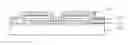
Referred to FIGS. 1(a) and 1(b), a signal line metal layer is deposited on the whole glass substrate 10, and a pattern of a first mask is formed on a photo-resist layer by performing the first coating, exposing and developing, and a signal line metal electrode 11 is formed by performing the first etching and removing the photo-resist, wherein the signal line metal electrode 11 is a ring shape electrode.
Referred to FIGS. 2(a) and 2(b), a passivation layer 21 is deposited on the whole glass substrate 10, a pattern of a second mask is formed on the photo-resist layer by performing the second coating, exposing and developing, and a passivation layer 21 is formed by performing the second etching to remove the passivation layer on the signal line metal layer and remove the photo-resist, and a square shape via hole 22 is formed on the signal line metal electrode 11.
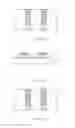
Referred to FIGS. 3(a) and 3(b), a transparent conductive layer 21 is deposited on the whole glass substrate 10, the transparent conductive layer is generally an ITO layer. A pattern of a third mask is formed on the photo-resist layer by performing the third coating, exposing and developing, and ITO electrodes which are alternately arranged are formed by performing the third etching and removing the photo-resist. The ITO electrode is a stripe shape electrode and the ITO electrode 31 is coupled to the signal line metal electrode 11 through the square shape via hole 22.
The above-described method of manufacturing a 3D barrier substrate may ensure that the ring shape signal line metal electrode 11 charges the stripe shape ITO transparent electrode 31 respectively, and the design requirements for a 3D barrier substrate are met
To sum up, in the prior art, the method of manufacturing a 3D barrier substrate need to perform a photo etching process for three times and adopts a three-layer structure comprising a signal line metal layer, a passivation layer, and an ITO transparent conducting layer, and each of which need to design a mask respectively, so many procedures decreases the production efficiency and increases the cost of production.
SUMMARY
An embodiment according to the present invention provides a 3D barrier substrate, a method of manufacturing the same, and a display device to improve the utilization of facilities, increase the production efficiency, and decrease the cost of production.
An embodiment according to the present invention provides a method of manufacturing a 3D barrier substrate comprising:
forming a transparent electrode thin film on a substrate, and forming a passivation layer on the transparent electrode thin film;
forming an transparent electrode and a passivation layer via hole by a patterning process, wherein the via hole is used for coupling the transparent electrode to a signal line; and
forming the signal line, wherein the signal line is coupled to the transparent electrode through the via hole.
An embodiment according to the present invention provides a 3D barrier substrate comprising: a substrate, a transparent electrode on the substrate, a passivation layer on the transparent electrode layer, and a signal line on the passivation layer, wherein the signal line is coupled to the transparent electrode through a via hole on the passivation layer.
An embodiment according to the present invention provides a display device comprising the above-described 3D barrier substrate.
To sum up, among the technical solutions provided by the embodiments of the present invention, the method of manufacturing a 3D barrier substrate comprises: forming a transparent electrode thin film on a substrate, and forming a passivation layer on the transparent electrode thin film; forming an transparent electrode and a passivation layer via hole by a patterning process, wherein the via hole is used for coupling the transparent electrode to the signal line; and forming a signal line, wherein the signal line couples to the transparent electrode through the via hole. The method provided by the embodiment of the present invention adopts two times patterning process, decreases the cost of producing the mask, reduces one time exposure process, shortens the process procedure, improves the utilization of facilities, increases the production efficiency, and decreases the cost of production
BRIEF DESCRIPTION OF THE DRAWINGS
FIGS. 1(a) and 1(b) are a cross-section diagram and a front-view diagram of a signal line metal electrode manufactured in the prior art respectively;
FIGS. 2(a) and 2(b) are a cross-section diagram and a front-view diagram of the passivation layer manufactured on the basis of FIG. 1 in the prior art respectively;
FIGS. 3(a) and 3(b) are a cross-section diagram and a front-view diagram of the ITO electrode manufactured on the basis of FIG. 2 in the prior art respectively;
FIG. 4 is a flowchart showing the method of manufacturing a 3D barrier substrate according to an embodiment of the present invention;
FIGS. 5(a) and 5(b) are a cross-section diagram and a front-view diagram of the ITO layer and the passivation layer after depositing according to an embodiment of the present invention respectively;
FIGS. 6(a) and 6(b) are a cross-section diagram and a front-view diagram of a first photo-resist layer and a second photo-resist layer manufactured by coating the photo-resist and exposing and developing the photo-resist with a half exposure mask on the basis of FIG. 5 according to an embodiment of the present invention;
FIGS. 7(a) and 7(b) are a cross-section diagram and a front-view diagram after etching the passivation layer which is not coated by the photo-resist on the basis of FIG. 6 according to an embodiment of the present invention;
FIGS. 8(a) and 8(b) are a cross-section diagram and a front-view diagram after removing the second photo-resist layer on the basis of FIG. 7 according to an embodiment of the present invention;
FIGS. 9(a) and 9(b) are a cross-section diagram and a front-view diagram of the ITO electrode manufactured on the basis of FIG. 8 according to an embodiment of the present invention;
FIGS. 10(a) and 10(b) are a cross-section diagram and a front-view diagram after etching the passivation layer which is formerly coated by the second photo-resist layer on the basis of FIG. 9 according to an embodiment of the present invention;
FIGS. 11(a) and 11(b) are a cross-section diagram and a front-view diagram after removing the first photo-resist layer and depositing the signal line metal electrode on the basis of FIG. 10 according to an embodiment of the present invention;
FIGS. 12(a) and 12(b) are a cross-section diagram and a front-view diagram after coating the third photo-resist layer on the signal line metal electrode and then exposing and developing on the basis of FIG. 11 according to an embodiment of the present invention;
FIGS. 13(a) and 13(b) are a cross-section diagram and a front-view diagram of the signal line metal electrode manufactured on the basis of FIGS. 12 according to an embodiment of the present invention.
DETAILED DESCRIPTION
An embodiment of the present invention provides a 3D barrier substrate and a method of manufacturing the same, and a display device to improve the utilization of facilities, increases the production efficiency, and decrease the cost of production
The details of the technical solutions provided by the embodiments of present invention are described as follows.
Referred to FIG. 4, the method of manufacturing a 3D barrier substrate provided by an embodiment of the present invention comprises following steps:
S101: forming a transparent electrode thin film on a substrate, and forming a passivation layer on the transparent electrode thin film;
S102: forming a transparent electrode and a passivation layer via hole by a patterning process, and the via hole being used to couple the transparent electrode to a signal line;
It is appreciated that the patterning process may comprise a part or all processes of masking, exposing, developing, photo-etching, etching and so on which are required to form a pattern, and may also comprise ashing and annealing and so on.
For example, forming a pattern of a gate electrode on the substrate by a patterning process comprises: firstly, depositing a gate electrode layer on the substrate; then coating the photo-resist, and exposing and developing the photo-resist using a mask so as to form a photo-resist pattern; then, removing a corresponding electrode layer by etching process and so on by using the photo-resist pattern as an etching mask, and removing the residual photo-resist; and finally forming the gate electrode pattern on the substrate.
S103: forming the signal line which is coupled to the transparent electrode through a via hole.
Preferably, the patterning process comprises: a part or all processes of a photo etching process of coating a photo-resist on the passivation layer and then exposing and developing, a etching process after photo-etching, and a process of removing the photo-resist after etching.
Preferably, when a transparent electrode and a passivation layer via hole are formed by the patterning process, after exposing and developing the photo-resist coated on the passivation layer by a halftone technique, the photo-resist layer coated on the passivation layer comprises: a first photo-resist layer which coats a region where the transparent electrode is to be formed, a second photo-resist layer which coats a region where the via hole is to be formed, the via hole is used to couple the transparent electrode to the signal line, and the thickness of the first photo-resist layer is larger than that of the second photo-resist layer.
Preferably, the process of forming the via hole comprises: etching the passivation layer which is not coated by the photo-resist, removing the second photo-resist layer, forming the transparent electrode by etching the revealed transparent electrode layer, and forming the via hole by etching the passivation layer that is formerly coated by the second photo-resist layer.
Preferably, the thickness of the first photo-resist layer is in the range of 1.5-3 μm, and the thickness of the second photo-resist layer is in the range of 0.5-1 μm.
Preferably, when removing the second photo-resist layer, the photo-resist having the thickness of 0.5-1 m is removed from the first photo-resist layer.
Preferably, the second photo-resist layer is removed by an ashing process.
Preferably, the process of forming the transparent electrode by etching the revealed transparent electrode layer comprises: performing over-etching when the revealed transparent electrode layer is etched, and the transparent electrode formed after over-etching has an indentation with a size of 0.5-2 μm relative to the passivation layer coating the transparent electrode so that the signal line may be only coupled to the transparent electrode through the via hole.
Preferably, the process of forming the signal line comprises: depositing a signal line metal layer, coating a third photo-resist layer on the signal line metal layer, and forming a pattern which is required by the signal line on the third photo-resist layer by exposing and developing, etching the signal line metal layer which is not coated by the third photo-resist layer, and forming the signal line by removing the third photo-resist layer.
The embodiments will be described in detail.
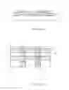
As shown in FIGS. 5(a) and 5(b), firstly, the transparent conductive layer 31 and the passivation layer 21 are sequentially deposited on the substrate 10, wherein the substrate 10 is a glass substrate, the transparent electrode layer 31 is an ITO transparent conductive thin film layer. The ITO layer 31 and the passivation layer 21 are deposited in a low temperature by sputtering, wherein the deposition temperature is between a room temperature to 50° C., the deposition thickness of the ITO layer 31 is about between 400 to 800 Å, the deposition thickness of the passivation layer 21 is about between 2000 to 6000 Å. Furthermore, the ITO layer 31 may be deposited by a method of electron beam evaporation and so on, and the passivation layer 21 may be deposited by a method of Plasma Chemical Vapor Deposition (PCVD) and so on.
The detail of forming the transparent electrode and the passivation layer via hole by a patterning process is described as follows.
As shown in FIGS. 6(a) and 6(b), the photo-resist is coated on the passivation layer 21 evenly, the first photo-resist layer 51 and the second photo-resist layer 52 are formed on the passivation layer after the photo-resist is exposed and developed using a half exposure mask, wherein the first photo-resist layer 51 coats a region where the ITO electrode pattern is required to be formed, and the second photo-resist layer 52 coats a region where the via hole coupling the ITO electrode to the signal line is required to be formed, and the thickness of the first photo-resist layer 51 is larger than that of the second photo-resist layer 52. In an embodiment of the present invention, the thickness of the first photo-resist layer 51 is in a range of about 1.5-3 μm, and the thickness of the second photo-resist layer 52 is in a range of about 0.5-1 μm. However, the thickness of the first photo-resist layer 51 and the thickness of the second photo-resist layer 52 are not limited to the values presented in this invention, and may be adjusted according to an actual process. Wherein in the subsequent etching process, in the region which is not coated by the photo-resist, the ITO layer and the passivation layer are completely etched. In the subsequent etching process, in the region which is coated by the second photo-resist layer 52, the ITO layer 31 is kept and the passivation layer is completely etched. In the subsequent etching process, in the region that is coated by the first photo-resist layer 51, the passivation layer 21 and the ITO layer 31 are kept.
As shown in FIGS. 7(a) and 7(b), the passivation layer which is not coated by the photo-resist is etched and removed by dry etching so as to reveal the ITO layer 31 under the passivation layer 21.
As shown in FIGS. 8(a) and 8(b), the second photo-resist layer is removed by an ashing and photo-resist removing process so as to reveal the passivation layer 21 coated by the second photo-resist layer, and the first photo-resist layer 51 becomes thinner during this process, such as the thickness of the first photo-resist layer 51 is reduced by 0.5-1 μm.
As shown in FIGS. 9(a) and 9(b), the revealed ITO layer is etched by wet etching so as to form the desirable ITO electrode pattern 31. Wherein the ITO layer which is coated by the first photo-resist layer 51 and the passivation layer 21 is not etched.
Preferably, over-etching is required during the etching process. After over-etching, the ITO layer 31 has an indentation region 80 with a size of 0.5-2 μm relative to the passivation layer 21 coating the ITO layer 31 so that the ITO layer 31 and the metal layer are not electrically connected when depositing the metal layer subsequently.
As shown in FIGS. 10(a) and 10(b), the revealed passivation layer which is not coated by the photo-resist is etched by the second dry-etching so as to form the via hole 101 and reveal the ITO electrode 31,wherein the revealed ITO electrode 31 is located in the display area of the substrate.
As shown in FIGS. 11(a) and 11(b), the first photo-resist layer is removed and the ITO layer 31 is annealed. The conditions of annealing are: in the protective gas such as N2, O2 and so on, the temperature of annealing is in a range of 250° C-300° C., and the time period of annealing is in a range of 15-30 minutes. Wherein conditions of annealing are not limited to the conditions of annealing provided by the embodiment of the present invention. The conditions such as temperature of annealing, the time period of annealing and so on can be properly adjusted according to the actual process.
Then, the signal line metal layer 11 which has a thickness about 2000-5000 Å is deposited by sputtering, wherein the signal line metal layer 11 may also be deposited by other methods such as electron beam evaporation and so on.
The signal line is formed by the second patterning process, and the signal line may be only coupled to the transparent electrode through the via hole. Certainly, the second patterning process may be not exactly the same as the preceding pattering process. For example, the detail of the second patterning process may be described as following.
As shown in FIGS. 12(a) and 12(b), a third photo-resist layer 53 is coated on the signal line metal layer 11, and after exposing and developing, the pattern on the third photo-resist layer 53 is formed as required by the signal line 11. In the region where the third photo-resist layer 53 is coated, the signal line metal layer 11 is kept in the subsequent etching process.
As shown in FIGS. 13(a) and 13(b), the signal line metal layer which is coated by the third photo-resist layer 53 is etched by wet-etching, and then the third photo-resist layer 53 is removed by a striping method so as to form the required signal line 11. In the display area of the substrate, the ITO electrode lines 31 having different functionalities are coupled to the corresponding signal lines 11 respectively through the via holes so that the same signal is applied to the alternately arranged ITO electrode lines 31.
An embodiment of the present invention provides a 3D barrier substrate comprising: a substrate, a transparent electrode on the substrate, a passivation layer on the transparent electrode layer, and a signal line on the passivation layer, wherein the signal line is coupled to the transparent electrode through the via hole on the passivation layer.
Preferably, the transparent electrode, which is revealed at the position of the via hole on the passivation layer, is in the display area of the substrate.
Preferably, the transparent electrodes are alterately arranged transparent electrodes.
Preferably, the signal line is a ring shape signal line, and the transparent electrode is a strip shape transparent electrode.
Preferably, the transparent electrode is an Indium Tin Oxide transparent electrode.
An embodiment of the present invention provides a display device comprising the 3D barrier substrate, wherein the display device may be a liquid crystal display (LCD) or a naked-eye 3D display.
To sum up, among the technical solutions provided by the embodiments of the present invention, the method of manufacturing a 3D barrier substrate comprises: forming a transparent electrode thin film on a substrate, and forming a passivation layer on the transparent electrode thin film; forming an transparent electrode and a passivation layer via hole by a patterning process, wherein the via hole is used for coupling the transparent electrode to the signal line; and forming a signal line, wherein the signal line couples to the transparent electrode through the via hole. The method provided by the embodiment of the present invention adopts two times patterning process, decreases the cost of producing the mask, reduces one time exposure process, shortens the process procedure, improves the utilization of facilities, increases the production efficiency, and decreases the cost of production.
It should be noted that, those of ordinary skills in the art may further make improvements and modifications without departing from the principle of the present invention, and these improvements and modifications shall also be considered as the scope of the present invention.
Claims
1. A method for manufacturing a three-dimensional (3D) barrier substrate, comprising:
forming a transparent electrode thin film on a substrate, and forming a passivation layer on the transparent electrode thin film;
forming a transparent electrode and a passivation layer via hole by a patterning process, wherein the via hole is used for coupling the transparent electrode to a signal line; and
forming the signal line, wherein the signal line is coupled to the transparent electrode through the via hole.
2. The method according to claim 1, wherein the patterning process comprises:
a part or all processes of a photo etching process of coating photo-resist on the passivation layer and then exposing and developing the photo-resist, an etching process after photo-etching, and a process of removing the photo-resist after etching.
3. The method according to claim 1, wherein when the transparent electrode and the passivation layer via hole are formed by the patterning process, after exposing and developing the photo-resist coated on the passivation layer by a halftone technique, the photo-resist layer coated on the passivation layer comprises:
a first photo-resist layer and a second photo-resist layer, wherein the first photo-resist photo-resist layer coats a region where a transparent electrode pattern is to be formed, and the second photo-resist layer coats a region where the via hole is to be formed, the via hole is used to couple the transparent electrode to the signal line, and the thickness of the first photo-resist layer is larger than that of the second photo-resist layer.
4. The method according to claim 1, wherein the process of forming the via hole comprises:
etching the passivation layer which is not coated by the photo-resist,
removing the second photo-resist layer,
forming the transparent electrode by etching the revealed transparent electrode layer, and
forming the via hole by etching the passivation layer that is formerly coated by the second photo-resist layer.
5. The method according to claim 3, wherein
the thickness of the first photo-resist layer is in the range of 1.5-3 μm, and the thickness of the second photo-resist layer is in the range of 0.5-1 μm.
6. The method according to claim 4, wherein, when removing the second photo-resist layer, the photo-resist having the thickness of 0.5-1 μm is removed from the first photo-resist layer.
7. The method according to claim 4, wherein
the second photo-resist layer is removed by an ashing process.
8. The method according to claim 4, wherein
the process of forming the transparent electrode by etching the revealed transparent electrode layer comprises:
performing over-etching when the revealed transparent electrode layer is etched, and the transparent electrode formed after over-etching has an indentation relative to the passivation layer coating the transparent electrode, so that the signal line is only coupled to the transparent electrode through the via hole.
9. The method according to claim 1, wherein forming the signal line comprises:
depositing a signal line metal layer,
coating a third photo-resist layer on the signal line metal layer, and forming a pattern which is required by the signal line on the third photo-resist layer by exposing and developing,
etching the signal line metal layer which is not coated by the third photo-resist layer, and forming the signal line by removing the third photo-resist layer.
10. A three-dimensional (3D) barrier substrate comprising:
a substrate,
a transparent electrode on the substrate,
a passivation layer on the transparent electrode layer, and
a signal line on the passivation layer, wherein the signal line is coupled to the transparent electrode through a via hole on the passivation layer.
11. The 3D barrier substrate according to claim 10, wherein
the transparent electrode, which is revealed at the position of the via hole on the passivation layer, is in a display area of the substrate.
12. The 3D barrier substrate according to claim 10, wherein transparent electrodes are alternately arranged transparent electrodes.
13. The 3D barrier substrate according to claim 10, wherein
the signal line is a ring shape signal line, and the transparent electrode is a strip shape transparent electrode.
14. The 3D barrier substrate according to claim 10, wherein
the transparent electrode is an Indium Tin Oxide transparent electrode.
15. A display device comprising the three-dimensional (3D) barrier substrate according to claim 10.
16. The method according to claim 3, wherein the process of forming the via hole comprises:
etching the passivation layer which is not coated by the photo-resist,
removing the second photo-resist layer,
forming the transparent electrode by etching the revealed transparent electrode layer, and
forming the via hole by etching the passivation layer that is formerly coated by the second photo-resist layer.
17. The method according to claim 8, wherein the indentation has a size of 0.5-2 μm.
Images & Drawings included:


Sources:
- United States Patent and Trademark Office - verify current appl. status at the USPTO↗
Recent applications in this class:
- » 20250070107 2025-02-27
Electrode Comprising a Plurality of Deformable, Proximally-Diverging Electroconductive Protrusions - » 20240429360 2024-12-26
CURRENT COLLECTOR, SECONDARY BATTERY, ELECTRONIC DEVICE, AND MANUFACTURING METHOD THEREOF - » 20240405189 2024-12-05
ELECTRODE SHEET FOR LITHIUM ION BATTERY - » 20240332478 2024-10-03
BI-POLAR LITHIUM-ZINC-ION BATTERIES - » 20240113273 2024-04-04
Lithium-ion battery of fast-charging capability - » 20230395771 2023-12-07
Electrochemical cells having semi-solid electrodes and methods of manufacturing the same - » 20230246154 2023-08-03
CURRENT COLLECTOR, SECONDARY BATTERY, ELECTRONIC DEVICE, AND MANUFACTURING METHOD THEREOF - » 20230170457 2023-06-01
RECHARGEABLE LITHIUM BATTERY - » 20220320477 2022-10-06
BATTERY CELL, BATTERY, AND ELECTRIC DEVICE - » 20210167351 2021-06-03
Electrochemical cells having semi-solid electrodes and methods of manufacturing the same
Recent applications for this Assignee:
- » 20250295022 2025-09-18
QUANTUM DOT COMPOSITION, LIGHT-EMITTING ELEMENT, DISPLAY PANEL AND PREPARATION METHOD THEREOF - » 20250295019 2025-09-18
HEAT DISSIPATION FILM, DISPLAY MODULE AND DISPLAY DEVICE - » 20250294987 2025-09-18
DISPLAY PANEL, DISPLAY DEVICE - » 20250294983 2025-09-18
DISPLAY PANEL AND DISPLAY DEVICE - » 20250292736 2025-09-18
DRIVING CIRCUIT, DRIVING METHOD, DRIVING MODULE AND DISPLAY DEVICE - » 20250291336 2025-09-18
COMPUTER-IMPLEMENTED METHOD, APPARATUS FOR MANAGING PRODUCTION OF ONE OR MORE PRODUCTS, AND COMPUTER-PROGRAM PRODUCT - » 20250291215 2025-09-18
CIRCUIT BOARD AND METHOD FOR MANUFACTURING THE SAME, LIGHT-EMITTING SUBSTRATE, BACKLIGHT MODULE, DISPLAY PANEL AND DISPLAY APPARATUS - » 20250287801 2025-09-11
ARRAY SUBSTRATE AND DISPLAY APPARATUS - » 20250287695 2025-09-11
ARRAY PANEL, METHOD OF MANUFACTURING THE SAME AND DISPLAY DEVICE - » 20250287695 2025-09-11
ARRAY PANEL, METHOD OF MANUFACTURING THE SAME AND DISPLAY DEVICE