Method for generating clock for system operating at rising edge
US20150214941A1
2015-07-30
14/524,508
2014-10-27
✅ Patent granted
US 9,203,388 B2
2015-12-01
-
-
An Luu
Lee, Hong, Degerman, Kang & Waimey
2034-10-27
Abstract:
A method of converting an input clock to generate an output clock and providing a certain system with the output clock is provided. The method includes setting up a desired output clock value and a variable value and determining whether the input clock is the rising edge; adding the output clock value to the variable value to provide a calculated value when the input clock is the rising edge; comparing the calculated value with the input clock value; and outputting, when the calculated value is equal to or larger than the input clock value as a result of comparison, the output clock as logic state ‘1’ and setting, a value obtained by subtracting the input clock value from the calculated value, as the variable value.
Assignee:
- LSIS CO., LTD. 661 🇰🇷 Anyang-si, South Korea
- LSIS CO., LTD. 557 🇰🇷 Anyang-si, Gyeonggi-do, South Korea
Applicant:
Interested in similar patents?
Get notified when new applications in this technology area are published.
Classification:
H03K5/1534 » CPC main
Manipulating of pulses not covered by one of the other main groups of this subclass; Arrangements in which a pulse is delivered at the instant when a predetermined characteristic of an input signal is present or at a fixed time interval after this instant Transition or edge detectors
H03K5/135 IPC
Manipulating of pulses not covered by one of the other main groups of this subclass; Arrangements having a single output and transforming input signals into pulses delivered at desired time intervals by the use of time reference signals, e.g. clock signals
H03K23/68 » CPC further
Pulse counters comprising counting chains; Frequency dividers comprising counting chains with a base or radix other than a power of two with a base which is a non-integer
G06F1/08 » CPC further
Details not covered by groups - and; Generating or distributing clock signals or signals derived directly therefrom Clock generators with changeable or programmable clock frequency
Description
CROSS-REFERENCE TO RELATED APPLICATIONS
Pursuant to 35 U.S.C. §119(a), this application claims the benefit of earlier filing date and right of priority to Korean Patent Application No. 10-2014-0009486, filed on Jan. 27, 2014, the contents of which are hereby incorporated by reference herein in its entirety.
BACKGROUND
The present disclosure relates to a method of generating a clock operating at a rising edge and more particularly, to a method of generating a clock signal in a simple structure at high precision.
The clock signal is a square wave signal in which logic states ‘1’ and ‘0’ are regularly represented. In a general system, a clock has a certain duty ratio and the system is synchronized with the clock to process various signals.
A clock generation device may be a device that generates a clock having a certain duty ratio to be used in a system and may include a PLL circuit. However, the PLL circuit has limitations in that its logic is complex and it needs many transistors.
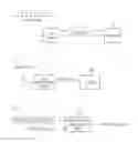
FIG. 1 shows how to provide a system needing a clock having a certain duty ratio with a clock.
Referring to FIG. 1, a PLL circuit 11 adjusts an input clock and generates an output clock suitable for a system 12. In this case, the PLL circuit may be implemented in both hardware and software, and since a hardware PLL structure has high precision but is complex in logic structure, it needs many transistors. On the contrary, a software-type PLL structure has a limitation in that it is difficult to ensure the precision of an output clock.
Also, in order to provide a system with a clock having a certain duty ratio, a clock adjustment by the PLL circuit is needed but a system that operates only at the rising edge or falling edge of the clock does not need a PLL circuit having a complex structure. Thus, in a system that needs a clock without a certain duty ratio, generating the clock precisely is needed.
SUMMARY
Embodiments provide a method of generating a clock at high precision through a simple structure, in the case of a system that operates in the rising edge of the clock.
In one embodiment, a method of converting an input clock to generate an output clock and providing a certain system with the output clock includes setting up a desired output clock value and a variable value and determining whether the input clock is the rising edge; adding the output clock value to the variable value to provide a calculated value when the input clock is the rising edge; comparing the calculated value with the input clock value; and outputting, when the calculated value is equal to or larger than the input clock value as a result of comparison, the output clock as logic state ‘1’ and setting, a value obtained by subtracting the input clock value from the calculated value, as the variable value.
The output clock value may be set to be smaller than the frequency of the input clock.
The determining of whether the input clock is the rising edge may include continually checking whether the input clock is the rising edge, when the input clock is not the rising edge.
When the calculated value is smaller than the input clock value as a result of comparison, the variable value may be set with the calculated value and then it may be checked whether the input clock is the rising edge.
When the calculated is equal to or larger than the input clock value, the output clock may be output with logic state ‘1’ and then with logic state ‘0’ at the rising edge of the input clock.
The variable value may be initially set to 0, and in this case, the output clock may be set as logic state ‘0’.
The method may further include determining whether the input clock is the rising edge, after the setting of the value obtained by subtracting the input clock value from the calculated value as the variable value.
The details of one or more embodiments are set forth in the accompanying drawings and the description below. Other features will be apparent from the description and drawings, and from the claims.
BRIEF DESCRIPTION OF THE DRAWINGS
FIG. 1 shows how to provide, a system needing a clock having a certain duty ratio, with a clock.
FIG. 2 shows an example of where a clock generation device according to an embodiment is used.
FIG. 3 shows a configuration of a clock generation device for a system operating at a rising edge according to an embodiment.
FIG. 4 is a flowchart of the operation of a clock generation device for a system operating at a rising edge according to an embodiment.
FIG. 5 is an exemplary waveform diagram of an output clock that is generated by a method of generating a clock for a system operating at a rising edge according to an embodiment.
DETAILED DESCRIPTION OF THE EMBODIMENTS
Reference will now be made in detail to embodiments of the present disclosure, examples of which are illustrated in the accompanying drawings.
FIG. 2 shows an example of where a clock generation device according to an embodiment is used, and FIG. 3 shows a configuration of a clock generation device for a system operating at a rising edge according to an embodiment.
Referring to FIGS. 2 and 3, a clock generation device according to an embodiment is applied to a system that operates by a rising edge. In addition, a clock generation device 110 changes an input clock to be suitable for a system 120 and provides the system 120 with a generated output clock.
In addition, the clock generation device 110 may include an output clock setup unit 11 and an output clock generation unit 113.
The output clock setup unit 111 is used for setting up an output clock to be provided for the system 120 and may be a user interface with which a user set up an output clock. For example, it may include an input screen that is shown on a display to be able to input an output clock, and an input unit such as a keyboard.
That is, a user may input a desired output clock to the input screen shown on the display by using a keyboard to set up the output clock.
In this case, since the output clock is generated by using the rising edge of an input clock in the present embodiment, the output clock may be set to be smaller than the input clock. In addition, the unit of a value set up for the output clock setup unit 111 is a frequency.
The output clock generation unit 113 changes the frequency of the input clock based on a setup value set by the output clock setup unit 111 and generates the output clock. The operation of the output clock generation unit 113 is described with reference to FIGS. 4 and 5.
FIG. 4 is a flowchart of the operation of a clock generation device for a system operating at a rising edge according to an embodiment.
Referring to FIG. 4, a desired output clock value N and a variable value N′ are firstly set up in step S110. In this case, the output clock value N is set up to be smaller than an input clock value M. In addition, the output clock value is set up through the output clock setup unit 111 and the variable value N′ is initially set to ‘0’.
Next, the output clock generation unit 113 receives the output clock value set up by the output clock setup unit 111 and an input clock, converts the frequency of the input clock based on the output clock value, then generates and outputs the output clock.
In particular, it is determined whether the input clock is a rising edge in step S120, and when negative, it is continually checked whether the input clock is the rising edge. In this case, the output clock is initially set with logic state ‘0’.
When it is determined that the input clock is the rising edge, the output clock generation unit 113 adds the variable value N′ to the output clock value N to generate a calculated value N″ in step S130.
Next, the input clock value M is compared with the calculated value N″ in step S140, and when the latter is smaller than the former (No in step S140), the variable value N′ is set with the calculated value N″ in step S150. In addition, it is again determined whether the input clock is the rising edge in step S120.
When the calculated value N″ is equal to or larger than the input clock value M (Yes in step S140), the output clock generation unit 113 generates the output clock of logic state ‘1’ for a certain time and sets, a value obtained by subtracting the input clock value M from the calculated value N″, as the variable value N′ in step S160.
Next, it is determined whether the input clock is the rising edge in step S120, and by repetitively performing such an operation, an output clock converted into a frequency set as an output setup value
A time period during which the logic state ‘1’ of the output clock is maintained is the same as the width of logic state ‘1’ of the input clock. That is, the output state of the output clock maintains logic state ‘1’ and then changes to logic state ‘0’ as at the falling edge of the input clock.
Thus, the output clock generation unit 113 maintains the output clock at logic state ‘1’ and outputs the output clock with logic state ‘0’ at the falling edge of the input clock, in step S170.
FIG. 5 is an exemplary waveform diagram of an output clock that is generated by a method of generating a clock for a system operating at a rising edge according to an embodiment.
FIG. 5 shows that the input clock value M is 300 MHz and the output clock value N is 100 MHz. When the first rising edge E_up1 of the input clock is input (Yes in step S120) while the output clock value N is initially set to 100 and the variable value N′ is initially set to 0 in step S110, the output clock value N ‘100’ is added to the variable value N″‘0’ to provide a calculated value N″ ‘100’ in step S130.
Next, the input clock value M ‘300’ is compared with the calculated value N″ ‘100’ in step S140, and since the latter M is smaller than the former N″ (No in step S140), the variable value N′ is set with the calculated value N″ in step S150. Thus, the variable value N′ becomes 100 and then it is determined whether the input clock is the rising edge in step S120.
Next, when the second rising edge E_up2 of the input clock is input, an output clock value N ‘100’ is added to the variable value N″100′ to provide a calculated value N″ ‘200’ in step S130.
Next, the input clock value M ‘300’ is compared with the calculated value N″ ‘200’ in step S140, and since the former M is larger than the latter N″ (No in step S140), the variable value N′ is set with the calculated value N″ in step S150, the variable value N′ becomes 200 and then it is determined whether the input clock is the rising edge in step S120.
Next, when the third rising edge E_up3 of the input clock is input, the output clock value N ‘100’ is added to the variable value N″200′ to provide a calculated value N″ ‘300’ in step S130. In addition, the input clock value M ‘300’ is compared with the calculated value N″ ‘300’ in step S140, and since the former M is equal to the latter N″ (Yes in step S140), the output clock is output as logic state ‘1’ and zero obtained by subtracting the input clock value M ‘300’ from the calculated value N″ ‘300’ is set as the variable value N′ in step S160.
Next, it is again determined whether the input clock is a rising edge in step S120, and as such a process is repeated, an output clock is generated.
The output clock maintains logic state ‘1’ and then logic state ‘0’ at the falling edge of the input clock in step S170.
Accordingly, when being applied to the generation of a clock for a system operating at a rising edge using only the rising edge of the clock without needing a certain duty ratio, it is possible to generate the clock without using a complex PLL. In addition, it is possible to ensure the precision of an output clock that a software-type PLL structure may not ensure.
Claims
What is claimed is:1. A method of generating a clock for a system operating at a rising edge, converting an input clock to generate an output clock and providing a certain system with the output clock, the method comprising:
setting up a desired output clock value and a variable value and determining whether the input clock is the rising edge;
adding the output clock value to the variable value to provide a calculated value when the input clock is the rising edge;
comparing the calculated value with the input clock value; and
outputting, when the calculated value is equal to or larger than the input clock value as a result of comparison, the output clock as logic state ‘1’ and setting, a value obtained by subtracting the input clock value from the calculated value, as the variable value.
2. The method according to claim 1, wherein the output clock value is set to be smaller than the frequency of the input clock.
3. The method according to claim 1, wherein the determining of whether the input clock is the rising edge comprises continually checking whether the input clock is the rising edge, when the input clock is not the rising edge.
4. The method according to claim 1, wherein when the calculated value is smaller than the input clock value as a result of comparison, the variable value is set with the calculated value and then it is checked whether the input clock is the rising edge.
5. The method according to claim 1, wherein when the calculated is equal to or larger than the input clock value, the output clock is output with logic state ‘1’ and then with logic state ‘0’ at the rising edge of the input clock.
6. The method according to claim 1, wherein the variable value is initially set to 0, and in this case, the output clock is set as logic state ‘0’.
7. The method according to claim 1, further comprising determining whether the input clock is the rising edge, after the setting of the value obtained by subtracting the input clock value from the calculated value as the variable value.
Images & Drawings included:


Sources:
- United States Patent and Trademark Office - verify current appl. status at the USPTO↗
Recent applications in this class:
- » 20250293677 2025-09-18
LOW-POWER SYNCHRONIZATION USING TRANSITION DETECTION - » 20250211217 2025-06-26
PHASE DIFFERENCE-BASED CALIBRATION USING MULTIPLE PHASE INTERPOLATORS - » 20250047271 2025-02-06
METHODS AND APPARATUS FOR CROSS-CONDUCTION DETECTION - » 20240030904 2024-01-25
Measuring pin-to-pin delays between clock routes - » 20230336167 2023-10-19
Methods and apparatus for cross-conduction detection - » 20230299759 2023-09-21
Glitch removal circuit - » 20230238949 2023-07-27
Techniques to reduce the effect of pad asymmetry and signal routing on resolution of PWM or PFM signals - » 20220294438 2022-09-15
Signal output circuit and circuit for outputting delayed signal - » 20220294437 2022-09-15
Pulse generation circuit and stagger pulse generation circuit - » 20220209760 2022-06-30
Measuring pin-to-pin delays between clock routes
Recent applications for this Assignee:
- » 20210194275 2021-06-24
Uninterruptible power supply system comprising energy storage system - » 20210152079 2021-05-20
Power conversion device utilizing a relay unit with multiple relays - » 20210111581 2021-04-15
Hybrid energy storage system - » 20200366101 2020-11-19
Energy storage system - » 20200312599 2020-10-01
Arc extinguishing unit of molded case circuit breaker - » 20200294744 2020-09-17
Coil control device of electronic magnetic contactor - » 20200280191 2020-09-03
Energy storage system - » 20200232711 2020-07-23
Heatsink module for inverter - » 20200228028 2020-07-16
Inverter system - » 20200220380 2020-07-09
Hierarchical power control system