Method, apparatus and system for level shifting of common mode voltage from input to output for capacitive feedback transimpedance amplifier
US20150256136A1
2015-09-10
14/642,602
2015-03-09
✅ Patent granted
US 9,489,098 B2
2016-11-08
-
-
Calvin C Ma
Frank D. Cimino
2035-04-10
Abstract:
A circuit for a level shifting of common mode voltage. The circuit includes a first amplifier, wherein the input of the first amplifier is coupled to a voltage source and another input of the first amplifier is coupled 2.5v, feedback resistor, Rfb, and feedback capacitor, Cfb, connected coupled to the voltage source, wherein other side of feedback resistor is coupled between two resistors, R2 and R2′, and wherein the other side of the feedback capacitor is coupled between R2′ and the output of the first amplifier, R2 is connected to Vbias from one side and Rfb and R2′ from the other, R2′ is connected to Rfb and R2 from one side and Cfb and output of the first amplifier from the other side, another resistor, R1, is connect to the output of the first amplifier, Cfb and R2′ from one side and R1′, yet another resistor, and input of amp2 from the other, a second amplifier, Amp2, is connected to the R1 and R1′ at one input and 1.5v at the other input, and wherein the output of the second amplifier is connected to R1′, and R1′ connects to one input of the second amplifier and the output of the second amplifier.
Inventors:
- Harish Venkataraman 16 🇺🇸 Wylie, TX, United States
- Karan Singh Jain 7 🇺🇸 Dallas, TX, United States
- Susan Ann Curtis 3 🇺🇸 Allen, TX, United States
Assignee:
- TEXAS INSTRUMENTS INCORPORATED 18,931 🇺🇸 Dallas, TX, United States
Applicant:
Interested in similar patents?
Get notified when new applications in this technology area are published.
Classification:
H03F3/04 » CPC main
Amplifiers with only discharge tubes or only semiconductor devices as amplifying elements with semiconductor devices only
G01D5/24 » CPC further
Mechanical means for transferring the output of a sensing member; Means for converting the output of a sensing member to another variable where the form or nature of the sensing member does not constrain the means for converting; Transducers not specially adapted for a specific variable using electric or magnetic means influencing the magnitude of a current or voltage by varying capacitance
H03F1/02 IPC
Details of amplifiers with only discharge tubes, only semiconductor devices or only unspecified devices as amplifying elements Modifications of amplifiers to raise the efficiency, e.g. gliding Class A stages, use of an auxiliary oscillation
G09G5/00 IPC
Control arrangements or circuits for visual indicators common to cathode-ray tube indicators and other visual indicators
G09G5/003 » CPC further
Control arrangements or circuits for visual indicators common to cathode-ray tube indicators and other visual indicators Details of a display terminal, the details relating to the control arrangement of the display terminal and to the interfaces thereto
H03F1/0205 » CPC further
Details of amplifiers with only discharge tubes, only semiconductor devices or only unspecified devices as amplifying elements; Modifications of amplifiers to raise the efficiency, e.g. gliding Class A stages, use of an auxiliary oscillation in transistor amplifiers
G09G2300/0404 » CPC further
Aspects of the constitution of display devices; Structural and physical details of display devices Matrix technologies
H03F2200/135 » CPC further
Indexing scheme relating to amplifiers there being a feedback over one or more internal stages in the global amplifier
H03F2200/144 » CPC further
Indexing scheme relating to amplifiers the feedback circuit of the amplifier stage comprising a passive resistor and passive capacitor
H03F2200/555 » CPC further
Indexing scheme relating to amplifiers A voltage generating circuit being realised for biasing different circuit elements
G06F3/047 » CPC further
Input arrangements for transferring data to be processed into a form capable of being handled by the computer; Output arrangements for transferring data from processing unit to output unit, e.g. interface arrangements; Input arrangements or combined input and output arrangements for interaction between user and computer; Arrangements for converting the position or the displacement of a member into a coded form; Digitisers, e.g. for touch screens or touch pads, characterised by the transducing means using sets of wires, e.g. crossed wires
G06F3/044 » CPC main
Input arrangements for transferring data to be processed into a form capable of being handled by the computer; Output arrangements for transferring data from processing unit to output unit, e.g. interface arrangements; Input arrangements or combined input and output arrangements for interaction between user and computer; Arrangements for converting the position or the displacement of a member into a coded form; Digitisers, e.g. for touch screens or touch pads, characterised by the transducing means by capacitive means
H03F2203/45101 » CPC further
Indexing scheme relating to amplifiers with only discharge tubes or only semiconductor devices as amplifying elements covered by; Indexing scheme relating to differential amplifiers Control of the DC level being present
H03F2203/45138 » CPC further
Indexing scheme relating to amplifiers with only discharge tubes or only semiconductor devices as amplifying elements covered by; Indexing scheme relating to differential amplifiers Two or more differential amplifiers in IC-block form are combined, e.g. measuring amplifiers
H03F2203/45526 » CPC further
Indexing scheme relating to amplifiers with only discharge tubes or only semiconductor devices as amplifying elements covered by; Indexing scheme relating to differential amplifiers the FBC comprising a resistor-capacitor combination and being coupled between the LC and the IC
H03F2203/45528 » CPC further
Indexing scheme relating to amplifiers with only discharge tubes or only semiconductor devices as amplifying elements covered by; Indexing scheme relating to differential amplifiers the FBC comprising one or more passive resistors and being coupled between the LC and the IC
G06F3/045 IPC
Input arrangements for transferring data to be processed into a form capable of being handled by the computer; Output arrangements for transferring data from processing unit to output unit, e.g. interface arrangements; Input arrangements or combined input and output arrangements for interaction between user and computer; Arrangements for converting the position or the displacement of a member into a coded form; Digitisers, e.g. for touch screens or touch pads, characterised by the transducing means using resistive elements, e.g. a single continuous surface or two parallel surfaces put in contact
H03F3/45 IPC
Amplifiers with only discharge tubes or only semiconductor devices as amplifying elements Differential amplifiers
H03F3/45475 » CPC further
Amplifiers with only discharge tubes or only semiconductor devices as amplifying elements; Differential amplifiers with semiconductor devices only characterised by the way of implementation of the active amplifying circuit in the differential amplifier using IC blocks as the active amplifying circuit
Description
CROSS REFERENCES TO RELATED APPLICATIONS
This application claims priority from U.S. Provisional Patent Application No. 61/949,391 filed on Mar. 7, 2014, which is hereby incorporated by reference in its entirety.
BACKGROUND OF THE INVENTION
1. Field of the Invention
Embodiments of the present invention generally relate to a method, apparatus and system for touch screen processing. More specifically, to a level shifting of common mode voltage from input to output for capacitive feedback transimpedance amplifier
2. Description of the Related Art
In a touch screen's amplifier configuration, the input of amplifier is capacitive. However, the amplifier configuration is required to be held at DC voltage different than output of the amplifier. As a result, a lot of DC current is wasted, which is inefficient, or another analog stage of amplifier is required, which comes at a cost of adding another source of noise to the system and its associated complexity.
Therefore, there is a need to hold the DC voltage without the extra stage or wasted DC power.
SUMMARY OF THE INVENTION
Embodiments of the present invention relate to a circuit for a level shifting of common mode voltage. The circuit includes a first amplifier, wherein the input of the first amplifier is coupled to a voltage source and another input of the first amplifier is coupled 2.5v, feedback resistor, Rfb, and feedback capacitor, Cfb, connected coupled to the voltage source, wherein other side of feedback resistor is coupled between two resistors, R2 and R2′, and wherein the other side of the feedback capacitor is coupled between R2′ and the output of the first amplifier, R2 is connected to Vbias from one side and Rfb and R2′ from the other, R2′ is connected to Rfb and R2 from one side and Cfb and output of the first amplifier from the other side, another resistor, R1, is connect to the output of the first amplifier, Cfb and R2′ from one side and R1′, yet another resistor, and input of amp2 from the other, a second amplifier, Amp2, is connected to the R1 and R1′ at one input and 1.5v at the other input, and wherein the output of the second amplifier is connected to R1′, and R1′ connects to one input of the second amplifier and the output of the second amplifier.
BRIEF DESCRIPTION OF THE DRAWINGS
So that the manner in which the above recited features of the present invention can be understood in detail, a more particular description of the invention, briefly summarized above, may be had by reference to embodiments, some of which are illustrated in the appended drawings. It is to be noted, however, that the appended drawings illustrate only typical embodiments of this invention and are therefore not to be considered limiting of its scope, for the invention may admit to other equally effective embodiments.
FIG. 1 is an embodiment of a circuit schematic of the prior art;
FIG. 2 is an embodiment of a graph depicting performance of the prior art;
FIG. 3 is an embodiment of a circuit schematic for a level shifting of common mode voltage;
FIG. 4 is an embodiment of a graph depicting performance of the circuit schematic of FIG. 3.
DETAILED DESCRIPTION
The proposed solution provides for a way of providing DC feedback which leads the amplifier to think it is regulating the same voltage both at the input and the output. The solution uses a common mode DC shift current inside the feedback loop, which maintains a different DC voltage at the output with respect to the input of the amplifier.
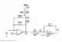
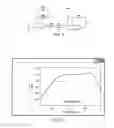
FIG. 1 is an embodiment of a circuit schematic of the prior art. The circuit comprises ample 1, amp 2, Rfb, Cfb, R1, R1′ and switch S1. The amp1 receives input from an input voltage source and 2.5 v. The amp1 is connected in series with Rfb and Cfb, where one lead of Rfb and Cfb is coupled to the voltage source and the other is coupled to the output of amp1. V1 is measures at the output of amp 1 to be 2.5v. R1 is connect in series at the output of amp 1. R1 is coupled to the output of amp1, R1′ on one side and R1′ and S1 on the other. S1 is coupled to R1, R1′ and amp2 from one side and Vbias one the other. R′1 is connected to the input of amp 2, R1 and Vbias; on the other side, R1′ is connected to the output of amp2. Amp2 has input voltage of 1.5 v on one lead and R1, R1′ and S1 on the other input lead. The output of amp2 is v2. FIG. 2 is an embodiment of a graph depicting performance of the prior art. The performance of this circuit is shown in the graph of FIG. 2 and is defined as follows:
| Characteristics | Performance |
| DC Power | Idc1 = (2.5 − 1.5)/R1 |
| If R1 5 Kohms → Then Idc1 = 200 uA/Amplifier | |
| If R1 40 Kohms → Then Idc1 = 25 uA/Amplifier | |
| Output-Dynamic | 4 Vpp |
| Range | |
| Area Impact | Require Vbias generation can be used for all the Amps |
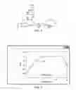
FIG. 3 is an embodiment of a circuit schematic for a level shifting of common mode voltage. The circuit comprises ample 1, amp 2, Rfb, Cfb, R1, R1′, R2, and R2′. One lead of amp1 is coupled to the voltage source and the other to 2.5v. One lead of Rfb and Cfb are connected to the voltage source. The other side of Rfb is connected between R2 and R2′. R2 is connected to Vbias from one side and Rfb and R2′ from the other. R2′ is connected to Rfb and R2 from one side and Cfb and output of amp1 from the other side. R1 is connect to the output of amp1, Cfb and R2′ from one side and R1′ and input of amp2 from the other. Amp2 is connected to the R1 and R1′ at one input, 1.5v at the other input and R1′ at its output. R1′ connects to one input of amp2 and the output of amp2. FIG. 4 is an embodiment of a graph depicting performance of the circuit schematic of FIG. 3. The performance of this circuit is shown in the graph of FIG. 4 and is defined as follows:
| Characteristics | Comments | |
| DC Power | Idc1 = 0; | |
| Idc2 = (2.5 − 1.5)/R2 ~= 100 Kohms | ||
| Then Idc2 = 10 uA/Amplifier | ||
| Output | 2 Vpp | |
| Dynamic | ||
| Range | ||
| Area Impact | Require Vbias generation can be used for all the | |
| Amps | ||
The improved solution between FIG. 1 and FIG. 3 does not require an increase DC power or noise of system and is simple and simple to implement.
While the foregoing is directed to embodiments of the present invention, other and further embodiments of the invention may be devised without departing from the basic scope thereof, and the scope thereof is determined by the claims that follow.
Claims
What is claimed is:1. A circuit for a level shifting of common mode voltage, comprising:
A first amplifier, wherein the input of the first amplifier is coupled to a voltage source and another input of the first amplifier is coupled 2.5v;
feedback resistor, Rfb, and feedback capacitor, Cfb, connected coupled to the voltage source, wherein other side of feedback resistor is coupled between two resistors, R2 and R2′, and wherein the other side of the feedback capacitor is coupled between R2′ and the output of the first amplifier;
R2 is connected to Vbias from one side and Rfb and R2′ from the other;
R2′ is connected to Rfb and R2 from one side and Cfb and output of the first amplifier from the other side;
another resistor, R1, is connect to the output of the first amplifier, Cfb and R2′ from one side and R1′, yet another resistor, and input of amp2 from the other;
a second amplifier, Amp2, is connected to the R1 and R1′ at one input and 1.5v at the other input, and wherein the output of the second amplifier is connected to R1′; and
R1′ connects to one input of the second amplifier and the output of the second amplifier.
2. The circuit for a level shifting of common mode voltage of claim 1, wherein R1 and R1′ have the same value.
3. The circuit for a level shifting of common mode voltage of claim 1, wherein R2 and R2′ have the same value.
4. The circuit for a level shifting of common mode voltage of claim 1, wherein the circuit is couple to a touch screen.
Images & Drawings included:
Sources:
- United States Patent and Trademark Office - verify current appl. status at the USPTO↗
Recent applications in this class:
- » 20250202441 2025-06-19
AMPLIFIER ARRANGEMENT AND METHOD FOR AMPLIFIER ARRANGEMENT WITH SET CURRENT AT CONTROL INPUT OF THE AMPLIFIER ARRANGEMENT IN DEPENDENCE ON AN OUTPUT CURRENT OF THE AMPLIFIER ARRANGEMENT - » 20250132735 2025-04-24
CIRCUITS FOR AMPLFICATION OF A DELTA-SIGMA MODULATED BIT-STREAM - » 20250119107 2025-04-10
BI-DIRECTIONAL AMPLIFIER DEVICE - » 20250105800 2025-03-27
METHODS AND APPARATUS TO IMPROVE AN OUTPUT OF AN AMPLIFIER - » 20250080061 2025-03-06
SEMICONDUCTOR DEVICE, AMPLIFIER AND BIASING CIRCUIT - » 20250080060 2025-03-06
AMPLIFIER WITH TRANSISTOR VOLTAGE CONTROL - » 20250070726 2025-02-27
Amplifier Auto-Zero Without Signal Switching - » 20240364278 2024-10-31
CASCODED HIGH-VOLTAGE AMPLIFIER - » 20240339967 2024-10-10
SEMICONDUCTOR AMPLIFIER CIRCUIT - » 20240213931 2024-06-27
INSTRUMENTATION AMPLIFIER WITH BASE CURRENT COMPENSATOR FOR IMPROVED PERFORMANCE
Recent applications for this Assignee:
- » 20250291595 2025-09-18
CIRCUIT, SYSTEM, AND METHOD FOR MATRIX DECIMATION - » 20250286550 2025-09-11
TRANSISTOR SHUTDOWN CIRCUT - » 20250279725 2025-09-04
CONDUCTION MODE CONTROL - » 20250274138 2025-08-28
SWITCH REGULATOR - » 20250267687 2025-08-21
ENHANCED BROADCAST TRANSMISSION IN UNSLOTTED CHANNEL HOPPING MEDIUM ACCESS CONTROL - » 20250266825 2025-08-21
BOOTSTRAP CIRCUIT - » 20250247097 2025-07-31
LEVEL SHIFTER CIRCUIT - » 20250247082 2025-07-31
LOW AREA AND POWER MULTI-BIT FLIP-FLOP - » 20250246995 2025-07-31
SWITCHING CONVERTER DEADTIME CONTROL - » 20250246345 2025-07-31
TRIMMING RESISTOR USING MODULATED SIGNAL