High dynamic range exponential current generator with MOSFETs
US20150286237A1
2015-10-08
14/243,741
2014-04-02
✅ Patent granted
US 9,176,513 B2
2015-11-03
-
-
Quan Tra
Richard C. Litman
2034-07-26
Abstract:
The high dynamic range exponential current generator produces an output waveform (current/voltage) which is an exponential function of the input waveform (current/voltage). The exponential characteristics are obtained in BiCMOS or Bipolar technologies using the intrinsic characteristics (IC/VBE) of the bipolar transistors. The high dynamic range exponential current generator is biased in weak inversion region. MOSFETs biased in weak inversion region are used not to utilize the inherent exponential (IDS/VGS) relationship but to simply implement x2 and x4 terms using translinear loops. The term x4 is realized by two cascaded squaring units. The approximation equation used is
x ≅ 0.025 + ( 1 + 0.125 x ) 4 0.025 + ( 1 - 0.125 x ) 4 .
Inventors:
- KARAMA M. AL-TAMIMI 3 🇸🇦 DHAHRAN, Saudi Arabia
- MUNIR A. AL-ABSI 19 🇸🇦 DHAHRAN, Saudi Arabia
Assignee:
- KING FAHD UNIVERSITY OF PETROLEUM AND MINERALS 2,608 🇸🇦 DHAHRAN, Saudi Arabia
Applicant:
Interested in similar patents?
Get notified when new applications in this technology area are published.
Classification:
G05F3/16 » CPC main
Regulating voltage or current wherein the variable is dc using uncontrolled devices with non-linear characteristics being semiconductor devices
G05F1/10 IPC
Automatic systems in which deviations of an electric quantity from one or more predetermined values are detected at the output of the system and fed back to a device within the system to restore the detected quantity to its predetermined value or values, i.e. retroactive systems Regulating voltage or current
Description
BACKGROUND OF THE INVENTION
1. Field of the Invention
The present invention relates to exponential generator circuits, and particularly to a high dynamic range exponential current generator utilizing MOSFETS operating in the weak inversion mode.
2. Description of the Related Art
An exponential function generator produces an output waveform (current/voltage) which is an exponential function of the input waveform (current/voltage). The exponential characteristics can be easily obtained in BiCMOS or Bipolar technologies using the intrinsic characteristics (IC/VBE) of the bipolar transistors. Though, it is not easy to realize such function in CMOS technology because of the inherent square-law or linear characteristics of MOSFETs operating in the strong inversion region. So the widely used technique to implement analog exponential function circuits using MOSFETs in strong inversion is based on pseudo-approximations. To mathematically implement the exponential function by this method, different approximations have been already introduced; Taylor series 2nd order, Taylor series 4th order, Pseudo exponential, Pseudo-Taylor approximation, Modified Pseudo-Taylor approximation, additional approximations have been proposed.
A MOSFET device biased in weak inversion region is a well-known approach to introduce an exponential function due to the exponential relationship between IDS and VGS of MOSFET in weak inversion regime. Referring to IDS/Vgs relationship, the drain current of MOSFET in weak inversion region is given by:
I DS = 2 n μ n C ox W L V T 2 ( V gs - V th nU T )
Although the low VGS voltage makes this technique efficient in low voltage applications compared with approximations that use MOSFET in strong inversion regime but, obviously, the exponential relation between IDS and VGS is not perfect because it suffers from strong temperature dependency, threshold voltage variation effect and sensitivity against process variation. Therefore, it is highly preferred to design an exponential function generator that provides accurate and stable exponential function vs. temperature variation; provides a robust and efficient design versus the supply voltage variation; utilizes current-input current-output exponential generator thereby providing higher frequencies of operation and wider dynamic ranges and extended output range with minimum linearity error.
Thus, a high dynamic range exponential current generator with MOSFETs solving the aforementioned problems is desired.
SUMMARY OF THE INVENTION
The high dynamic range exponential current generator produces an output waveform (current/voltage) which is an exponential function of the input waveform (current/voltage). The exponential characteristics are obtained in BiCMOS or Bipolar technologies using the intrinsic characteristics (IC/VBE) of the bipolar transistors. The high dynamic range exponential current generator is biased in weak inversion region. MOSFETs biased in weak inversion region are used not to utilize the inherent exponential (IDS/VGS) relationship but to simply implement x2 and x4 terms using translinear loops. The term x4 is realized by two cascaded squaring units. The approximation equation used is
x ≅ 0.025 + ( 1 + 0.125 x ) 4 0.025 + ( 1 - 0.125 x ) 4 .
These and other features of the present invention will become readily apparent upon further review of the following specification and drawings.
BRIEF DESCRIPTION OF THE DRAWINGS
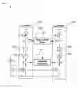
FIG. 1 is a block diagram of the high dynamic range exponential current generator according to the present invention.
FIGS. 2A-2C is a circuit diagram of the high dynamic range exponential current generator according to the present invention.
FIG. 3 is a circuit diagram of a squaring unit of the high dynamic range exponential current generator according to the present invention.
FIG. 4 is a circuit diagram of a single quadrant divider of the high dynamic range exponential current generator according to the present invention.
FIG. 5 is a circuit diagram of a current mirror of the high dynamic range exponential current generator according to the present invention.
FIG. 6 is a plot showing exact vs. proposed exponential approximation according to the present invention.
FIG. 7 is a plot showing exact vs. simulation results of the SQ block of the high dynamic range exponential current generator according to the present invention.
FIG. 8 is a plot showing BDCM error of the high dynamic range exponential current generator according to the present invention.
FIG. 9 is a plot showing effect of mismatch in the current mirror of the high dynamic range exponential current generator according to the present invention.
FIG. 10 is a plot showing linear-in-dB characteristics of the high dynamic range exponential current generator according to the present invention.
Similar reference characters denote corresponding features consistently throughout the attached drawings.
DETAILED DESCRIPTION OF THE PREFERRED EMBODIMENTS
The high dynamic range exponential current generator produces an output waveform (current/voltage) which is an exponential function of the input waveform (current/voltage). The exponential characteristics are obtained in BiCMOS or Bipolar technologies using the intrinsic characteristics (IC/VBE) of the bipolar transistors. The high dynamic range exponential current generator is biased in weak inversion region. MOSFETs biased in weak inversion region are used to simply implement x2 and x4 terms using translinear loops. The term x4 is realized by two cascaded squaring units 106. The exponential function generator approximation equation used is characterized by the relation,
x ≅ 0.025 + ( 1 + 0.125 x ) 4 0.025 + ( 1 - 0.125 x ) 4 . ( 1 )
and has a dynamic range of approximately 96 dB. Plot 700 of FIG. 7 shows exact vs. simulation results of the squaring unit 106.
The full block diagram of the present high dynamic range exponential current generator with MOSFETs 100 is shown in FIGS. 2A-2C. The number of transistors used in the overall circuit is 65 MOSFETs without any passive elements and all of them are stacked between ±0.75V voltage-supply.
The squaring unit 106 is shown in detail in FIG. 3. The voltage supply is ±0.75V and the aspect ratios of the transistors are illustrated in Table 1. The constant currents equal to 4 Iref and 1.6 Iref can be easily provided by a proper current source and current sink of current Iref; e.g. if the current Iref shown in FIG. 1 is set to be 25 nA, then the constant current 4 Iref flowing through M9 (shown in FIG. 3) will be 100 nA. With reference to the MOSFET circuitry of squaring unit 106, by applying Translinear Loop (TL) through transistors M1-M4 then,
Vgs1+Vgs2=Vgs3+Vgs4, (2)
where Vgs1, Vgs2, Vgs3 and Vgs4 are the gate-to-source voltages of M1, M2, M3 and M4 respectively. From equation (2), one obtains the following:
I1I2=I3I4. (3)
Since I1=I2=Ix, I3=4Iref and I4=Iout then the output current will be expressed as follows:
I out = I x 2 4 I ref . ( 4 )
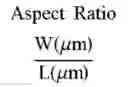
Equation (4) represents the current-mode squaring function. Since the squaring circuit 106 is a key block in the present current-mode exponential generator 100, the simulation results have been carried out to demonstrate the validity of the theory. The corresponding maximum error is 1.5% and the circuit is stable with temperature variation. Table 1 details the aspect ratios of the squaring unit.
| TABLE 1 |
| Aspect ratios of squaring unit |
| Transistor | Aspect Ratio W ( μm ) L ( μm ) | Ratio |
| M1, M3 | 3.5/7 | 0.5 |
| M2, M4 | 91.7/7 | 13.1 |
| M5-M10 | 7/7 | 1 |
With respect to the current divider 108, as shown in FIG. 4, the transistors involved in dashed box Ma-Md forms a single-quadrant current divider where all transistors are operating in the sub-threshold region. Analysis of the Ma-Md loop results in:
Vsga+Vsgb=Vsgc+Vsgd, (5)
IaIb=IcId, (6)
with Ia=Iw, Ib=0.125 Inum, Ic=0.125 Iden, and Id=Iout. Then the equation (6) becomes
I out , Divider = I w I num I den . ( 7 )
The transistor ratios are shown in Table 2. The
( W L ) j , l = 1 8 ( W L ) i , k
scale down the currents Inum and Iden so that transistors Mb (representing the dividend quantity) and Mc (representing the divisor quantity) can absorb this amount of current and as a result the quotient amount (represented by Md) can be improved in terms of accuracy. This implies that the aspect ratios of all the transistors involved in the translinear loop must be selected to meet the anticipated dynamic range of the input and output currents. Table 2 details the transistor dimensions of the single quadrant divider circuit 108.
| TABLE 2 |
| Transistor dimensions of the single quadrant divider circuit |
| Transistor | Aspect Ratio W ( μm ) L ( μm ) | Ratio |
| Ma, Md | 196/1.4 | 140 |
| Mb, Md | 175/1.4 | 125 |
| Me-Mh | 7/7 | 1 |
| Mi, Mk | 19.6/19.6 | 1 |
| Mj, Ml | 2.45/19.6 | 0.125 |
| Mm-Mn | 1/1 | 1 |
As shown in FIG. 5, the current mirror circuitry (CM) 110 has two output currents. If the input current is Ix then two copies of this current can obtained at the output, Ix and −Ix. The dimensions of CM 110 are listed in Table 3. The simulation results with ±0.75V voltage supply are shown to verify the functionality of the circuit. Plot 600 of FIG. 6 shows exact vs. the present exponential approximation. With respect to the DC transfer characteristics and transient response, the calculated error is very small, as shown in plot 800 of FIG. 8.
| TABLE 3 |
| Dimensions of CM |
| Transistor | Aspect Ratio W ( μm ) L ( μm ) | Ratio |
| Mn1-Mn5 | 1/10 | 0.1 |
| Mp1-Mp5 | 1.7/10 | 0.17 |
With reference to the present current mode exponential generator 100 as shown in FIG. 1, there are nodes A, B, C, D, E and F. The current flows through these nodes as follows:
I A = 8 I ref + I x = 8 I ref ( 1 + 0.125 I x I ref ) ( 8 ) I B = 8 I ref - I x = 8 I ref ( 1 - 0.125 I x I ref ) ( 9 ) I C = ( 8 I ref ) 2 ( 1 + 0.125 I x I ref ) 2 4 I ref ( 10 ) I D = ( 8 I ref ) 2 ( 1 - 0.125 I x I ref ) 2 4 I ref ( 11 ) I E = ( 8 I ref ) 4 ( 1 + 0.125 I x I ref ) 4 ( 4 I ref ) 3 = 64 I ref ( 1 + 0.125 I x I ref ) 4 ( 12 ) I F = ( 8 I ref ) 4 ( 1 - 0.125 I x I ref ) 4 ( 4 I ref ) 3 = 64 I ref ( 1 - 0.125 I x I ref ) 4 ( 13 ) I num = 1.6 I ref + 64 I ref ( 1 + 0.125 I x I ref ) 4 = 64 I ref [ 0.025 + ( 1 + 0.125 I x I ref ) 4 ] ( 14 ) I den = 1.6 I ref + 64 I ref ( 1 - 0.125 I x I ref ) 4 = 64 I ref [ 0.025 + ( 1 - 0.125 I x I ref ) 4 ] ( 15 )
By recall of the equations, the output current of the present EXPFG will be
I out = I w I num I den = I w { [ 0.025 + ( 1 + 0.125 I x I ref ) 4 ] [ 0.025 + ( 1 - 0.125 I x I ref ) 4 ] } ≅ I w ( I x I ref ) and , ( 16 ) I out = I w ( I x I ref ) , ( 17 )
where Iout is the output current, Ix is the input ac signal, Iref is a constant current and Iw is a DC component which can be used to scale the output signal. From equation (17), it is clear that the exponential current-mode generator can be realized and its output current can be adjusted by Iw. The full circuit of the present current-mode exponential function generator (EXPFG) 100 is shown in FIGS. 2A-2C.
Referring again to EXPFG 100 of FIG. 1, if the current mirror 1.6 Iref is not exact (i.e. it is equal to 1.6 Iref+ΔIref), then equations (14) to (16) can be reevaluated and the output current is expressed as:
I out = I w I num I den = I w { [ k + ( 1 + 0.125 I x I ref ) 4 ] [ k + ( 1 - 0.125 I x I ref ) 4 ] } , ( 18 )
where
k = 0.025 + Δ I ref 64 I den .
Assuming that there is ±10% deviation from the exact value (0.025), the results shown in plot 900 of FIG. 9 demonstrate that the deviation is not significant.
The EXPFG Circuit 100 shown in detail in FIGS. 2A-2C is used to implement the present function and is verified by simulation in 0.35 μm CMOS process technology with supply voltage ±0.75V. The threshold voltage of PMOS and NMOS is 0.833V and 0.572V in this process technology. The Tanner simulation result is illustrated in plot 1000 of FIG. 10 where Iref equals to 25 nA. Thus the x-axis, 150 nA≦Ix≦150 nA, can be normalized as −6≦x≦6 for comparison purposes. The curve of the present function is very close to the ideal exponential function,
I w ( I x 25 nA ) ,
with a high output dynamic range, nearly 96 dB. The error between the present function and the ideal exponential function,
I w ( I x 25 nA ) ,
is limited to ±0.5 dB when −137.5 nA≦Ix≦137.5 nA.
The simulation of transient response has been carried out with sinusoidal input signal of frequency 5 kHz. With respect to the results of normalized output current Iout (dB) at −25° C., +25° C. and +75° C., as expected the input\output characteristics are roughly stable with temperature variation. The linearity error remains less than ±1.5 dB for the full scale of the input current range. The maximum deviation of the output current was about ±1.27 dB and is occurred for the normalized value
I x I ref = 5.25 .
It is to be understood that the present invention is not limited to the embodiments described above, but encompasses any and all embodiments within the scope of the following claims.
Claims
We claim:1. A high dynamic range exponential current generator with MOSFETs, comprising:
a numerator current generator;
first and second numerator current generator squaring circuits connected in-line within the numerator current generator;
a denominator current generator;
first and second denominator current generator squaring circuits connected in-line within the denominator current generator;
a single quadrant divider circuit connected between output of the first numerator current generator squaring circuit and output of the first denominator current generator squaring circuit;
a bidirectional current mirror circuit connected between output of the second numerator current generator squaring circuit and output of the second denominator current generator squaring circuit;
numerator current generator and denominator current generator being biased in a weak inversion region that provides an approximation characterized by a relation,
x ≅ 0.025 + ( 1 + 0.125 x ) 4 0.025 + ( 1 - 0.125 x ) 4 ;
and
wherein all components of the exponential current generator are MOSFETs.
2. The high dynamic range exponential current generator with MOSFETs according to claim 1, wherein each of the squaring circuits further comprises a squaring circuit translinear loop consisting of first, second, third, and fourth squaring circuit translinear loop transistors, aspect ratio of first and third squaring circuit translinear loop transistors being approximately 0.5, aspect ratio of second and fourth squaring circuit translinear loop transistors being approximately 13.1, aspect ratio of non-translinear loop portion of the squaring circuit being approximately 1.
3. The high dynamic range exponential current generator with MOSFETs according to claim 2, wherein the single quadrant divider circuit further comprises:
a single quadrant divider circuit translinear loop consisting of first, second, third, and fourth single quadrant divider circuit translinear loop transistors, aspect ratio of first and fourth single quadrant divider circuit translinear loop transistors being approximately 140, aspect ratio of second and fourth single quadrant divider circuit translinear loop transistors being approximately 125, aspect ratio of non-translinear loop portion of the single quadrant divider circuit being approximately 1;
first, second, third and fourth VDD rail connected transistors having an aspect ratio of 1;
a VSS rail connected numerator current input following transistor of the single quadrant divider circuit;
a VSS rail connected denominator current input following transistor of the single quadrant divider circuit;
aspect ratio of the VSS rail connected numerator current input following transistor of the single quadrant divider circuit/VSS rail connected denominator current input following transistor of the single quadrant divider circuit being approximately 0.125;
a numerator current input transistor;
a denominator current input transistor;
aspect ratio of the numerator current input transistor/denominator current input transistor being approximately 1; and
first and second single quadrant divider output current transistors having their gates connected together, drain of the first single quadrant divider output current transistor having its drain connected to drain of the fourth single quadrant divider translinear loop transistor, the current output being taken from drain of the second single quadrant divider output current transistor, aspect ratio of the first/second single quadrant divider output current transistors being approximately 1.
4. The high dynamic range exponential current generator with MOSFETs according to claim 3, wherein the bidirectional current mirror circuit further comprises:
VDD rail connected transistors each having an aspect ratio of approximately 0.1; and
VSS rail connected transistors each having an aspect ratio of approximately 0.17.
Images & Drawings included:


Sources:
- United States Patent and Trademark Office - verify current appl. status at the USPTO↗
Recent applications in this class:
- » 20250076914 2025-03-06
VOLTAGE REGULATOR - » 20250013256 2025-01-09
REFERENCE CURRENT GENERATING CIRCUIT - » 20240192717 2024-06-13
POWER SUPPLY - » 20240103555 2024-03-28
Sensor mirror circuitry with reduced error compounding - » 20230324942 2023-10-12
Power management circuit - » 20210271279 2021-09-02
Power voltage selection circuit - » 20200319661 2020-10-08
Measuring internal voltages of packaged electronic devices - » 20200159270 2020-05-21
Back-gate biasing voltage divider topology circuit structure - » 20200081474 2020-03-12
Constant current circuit for suppressing transient variation in constant current - » 20200081473 2020-03-12
Measuring internal voltages of packaged electronic devices
Recent applications for this Assignee:
- » 20250292541 2025-09-18
SYSTEM AND METHOD TO DETECT ROAD ANOMALIES - » 20250289999 2025-09-18
LUMINESCENT PAINT CONTAINING UPCONVERSION PHOSPHOR - » 20250289755 2025-09-18
CURED CEMENT COMPOSITION CONTAINING A ZEOLITE - » 20250286384 2025-09-11
SYSTEM AND METHODS FOR INTELLIGENT STABILITY AND CONTROL OF FREQUENCY OF AN INTEGRATED HYBRID RENEWABLE ENERGY SYSTEM - » 20250286379 2025-09-11
LOAD FREQUENCY STABILIZATION USING OPTIMIZED MPC-(1+PIDN) CONTROLLER FOR HIGH ORDER INTERCONNECTED RENEWABLE ENERGY BASED POWER SYSTEMS - » 20250282987 2025-09-11
INCORPORATING IMIDAZOLE-BASED NANOMATERIAL INTO DRILLING FLUIDS FOR EFFECTIVE HYDROGEN SULFIDE SCAVENGING DURING DRILLING OPERATIONS - » 20250281950 2025-09-11
VESSEL CLEANING ROBOTIC SYSTEM - » 20250281910 2025-09-11
FIBROUS SILICA LANTHANUM OXIDE-BASED CATALYST FOR DRY REFORMING OF METHANE AND METHODS OF PREPARATION THEREOF - » 20250281899 2025-09-11
METAL-ORGANIC FRAMEWORKS BASED ON UiO-66 AND METHOD FOR DIRECT AIR CAPTURE OF CARBON DIOXIDE - » 20250281898 2025-09-11
METHOD FOR REMOVING AMMONIA FROM WASTEWATER