Self-referenced MRAM element and device having improved magnetic field
US20150287764A1
2015-10-08
14/437,362
2013-10-11
✅ Patent granted
US 9,461,093 B2
2016-10-04
WO; PCT/EP2013/071357; 20131011
WO; WO2014/063938; 20140501
Galina Yushina
Pearne & Gordon LLP
2033-10-11
Abstract:
Self-reference-based MRAM element including: first and second magnetic tunnel junctions, each having a magnetoresistance that can be varied; and a field line for passing a field current to vary the magnetoresistance of the first and second magnetic tunnel junctions. The field line includes a first branch and a second branch each branch including cladding. The first branch is arranged for passing a first portion of the field current to selectively vary the magnetoresistance of the first magnetic tunnel junction, and the second branch is electrically connected in parallel with the first branch and arranged for passing a second portion of the field current to selectively vary the magnetoresistance of the second magnetic tunnel junction. The self-referenced MRAM element and an MRAM device including corresponding MRAM elements can use a reduced field current.
Assignee:
- CROCUS Technology SA 1 🇫🇷 Grenobie, France
- CROCUS Technology SA 56 🇫🇷 Grenoble, France
Applicant:
Interested in similar patents?
Get notified when new applications in this technology area are published.
Classification:
H01L27/222 » CPC main
Devices consisting of a plurality of semiconductor or other solid-state components formed in or on a common substrate including components using galvano-magnetic effects, e.g. Hall effects; using similar magnetic field effects Magnetic non-volatile memory structures, e.g. MRAM
H01L27/22 IPC
Devices consisting of a plurality of semiconductor or other solid-state components formed in or on a common substrate including components using galvano-magnetic effects, e.g. Hall effects; using similar magnetic field effects
H01L43/08 » CPC further
Devices using galvano-magnetic or similar magnetic effects; Processes or apparatus specially adapted for the manufacture or treatment thereof or of parts thereof Magnetic-field-controlled resistors
H01L43/02 » CPC further
Devices using galvano-magnetic or similar magnetic effects; Processes or apparatus specially adapted for the manufacture or treatment thereof or of parts thereof Details
H01L43/10 » CPC further
Devices using galvano-magnetic or similar magnetic effects; Processes or apparatus specially adapted for the manufacture or treatment thereof or of parts thereof Selection of materials
G11C11/161 » CPC further
Digital stores characterised by the use of particular electric or magnetic storage elements; Storage elements therefor using magnetic elements using elements in which the storage effect is based on magnetic spin effect details concerning the memory cell structure, e.g. the layers of the ferromagnetic memory cell
G11C11/15 » CPC further
Digital stores characterised by the use of particular electric or magnetic storage elements; Storage elements therefor using magnetic elements using thin-film elements using multiple magnetic layers
G11C11/1675 » CPC further
Digital stores characterised by the use of particular electric or magnetic storage elements; Storage elements therefor using magnetic elements using elements in which the storage effect is based on magnetic spin effect; Auxiliary circuits Writing or programming circuits or methods
H01L27/226 » CPC further
Devices consisting of a plurality of semiconductor or other solid-state components formed in or on a common substrate including components using galvano-magnetic effects, e.g. Hall effects; using similar magnetic field effects; Magnetic non-volatile memory structures, e.g. MRAM comprising multi-terminal components, e.g. transistors
G11C11/16 » CPC further
Digital stores characterised by the use of particular electric or magnetic storage elements; Storage elements therefor using magnetic elements using elements in which the storage effect is based on magnetic spin effect
H01L27/228 » CPC further
Devices consisting of a plurality of semiconductor or other solid-state components formed in or on a common substrate including components using galvano-magnetic effects, e.g. Hall effects; using similar magnetic field effects; Magnetic non-volatile memory structures, e.g. MRAM comprising multi-terminal components, e.g. transistors of the field-effect transistor type
Description
FIELD
The present disclosure concerns a self-referenced magnetic random access memory (MRAM) element having a field line adapted to provide an improved magnetic field. The present disclosure further concerns a self-referenced MRAM device comprising the MRAM elements.
DESCRIPTION OF RELATED ART
Self-referenced MRAM devices comprise a plurality of MRAM cells sharing common conducting lines. In particular, the plurality of MRAM cells can share a field line being arranged for passing a field current for generating a magnetic field destined to the writing of the MRAM cells and/or to the reading of the MRAM cells.
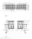
FIG. 1 illustrates a self-referenced MRAM element such as the one described in U.S. Pat. No. 8,031,519 by the present applicant. More particularly, the elevation view of FIG. 1 shows the MRAM element 1 comprising a first and second magnetic tunnel junction 2, 2′, a first strap 7 electrically connecting one end of the first magnetic tunnel junction 2 to a first CMOS selection transistor 8, and a second strap 7′ electrically connecting one end of the second magnetic tunnel junction 2′ to a second CMOS selection transistor 8′. The MRAM element further comprises a common field line 5 addressing the first and second magnetic tunnel junction 2, 2′, and a current line 3 connected to the other end of the first and second magnetic tunnel junction 2, 2′. In FIG. 1, the field line 5 is represented orthogonal to the page and perpendicular to the current line 3. FIG. 2 is a top view of a self-referenced MRAM device comprising a plurality of the MRAM elements 1. In the figure, the MRAM elements 1 are arranged in a row, along the field line 5. FIG. 3 represents another possible configuration of a MRAM element 1 where each magnetic tunnel junction 2 is connected to a current line 3 being arranged parallel to the field line 5.
In the above configurations of self-referenced MRAM elements, a magnetic field generated by the field current passing in the field line 5 varies a magnetoresistance of the magnetic tunnel junction 2, such that the MRAM element 1 can be written or read. Writing and/or reading the MRAM element requires passing the field current with a magnitude being high enough for the generated magnetic field to be able to vary/switch a magnetization of the magnetic tunnel junction 2. Indeed, the magnetic field should have a magnitude being typically comprised between 0 and 200 Oe, and preferably between 50 and 100 Oe.
In low power application, such as in mobile devices, high field currents are detrimental. The same applies for applications requiring a MRAM device having a high surface density of MRAM elements where high magnetic fields must be generated by small field lines.
Obtaining a self-referenced MRAM element and device wherein the field line is capable of generating a larger magnetic field for a given field current would thus be advantageous.
SUMMARY
The present disclosure concerns a self-reference-based MRAM element comprising a first magnetic tunnel junctions and a second magnetic tunnel junctions, each having a magnetoresistance that can be varied; and a field line for passing a field current destined to vary the magnetoresistance of the first and second magnetic tunnel junctions; the field line comprising a first branch and a second branch electrically connected in parallel with the first branch, the first branch being arranged for passing a first portion of the field current to selectively vary the magnetoresistance of the first magnetic tunnel junction, and the second branch being arranged for passing a second portion of the field current to selectively vary the magnetoresistance of the second magnetic tunnel junction.
In an embodiment, the first and second branches can be arranged so that a first portion of magnetic field generated by passing the first portion of field current in the first branch can only vary the magnetization of the first magnetic tunnel junction, and a second portion of magnetic field generated by passing the second portion of field current in the second branch can only vary the magnetization of the second magnetic tunnel junction.
In another embodiment, each of the first and second branches can comprise a cladding. Each of the first and second branches can have a rectangular cross section, and the cladding can be comprised on three sides of the rectangular cross section. The cladding can comprise a ferromagnetic material such as a NiFeCo alloy.
In yet another embodiment, the MRAM element can further comprise at least one current line electrically connected to one end each of the first and second magnetic tunnel junctions.
The present disclosure also concerns a MRAM device comprising a plurality of the MRAM elements. The plurality of the MRAM elements can be arranged in rows and columns, and the field line can extend along a row of MRAM elements with the first branch extending along the first magnetic tunnel junctions such as to selectively vary the magnetoresistance of the first magnetic tunnel junction of the MRAM elements in the row when the first portion of the field current is passed. The second branch can extend along the second magnetic tunnel junctions such as to selectively vary the magnetoresistance of the second magnetic tunnel junction of the MRAM elements in the row when the second portion of the field current is passed.
The disclosed self-referenced MRAM element and MRAM device can use a reduced field current in comparison to the one used in conventional self-referenced MRAM elements and devices. The magnetoresistance of the first and second magnetic tunnel junctions can also be varied with increased selectivity.
BRIEF DESCRIPTION OF THE DRAWINGS
The disclosure will be better understood with the aid of the description of an embodiment given by way of example and illustrated by the figures, in which:
FIG. 1 illustrates a conventional self-referenced MRAM element;
FIG. 2 is a top view of a self-referenced MRAM device comprising a plurality of the MRAM elements of FIG. 1;
FIG. 3 represents a conventional self-referenced MRAM element in another configuration;
FIG. 4 illustrates a self-referenced MRAM element, according to an embodiment;
FIG. 5 is a top view showing a self-reference MRAM device comprising a plurality of the MRAM elements, according to an embodiment; and
FIG. 6 represents the self-reference MRAM element according to another embodiment.
DETAILED DESCRIPTION OF POSSIBLE EMBODIMENTS
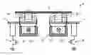
FIG. 4 illustrates an elevation view of a self-reference MRAM element 1 according to an embodiment. The MRAM element 1 comprises a first magnetic tunnel junction 2 and a second magnetic tunnel junction 2′, a field line 5 for passing a field current 51. The first and second magnetic tunnel junction 2, 2′ comprises a magnetoresistance that can be varied with an external magnetic field. In an embodiment not represented, the first and second magnetic tunnel junction 2, 2′ comprises a first ferromagnetic layer having a first magnetization that can be varied with the magnetic field, a barrier layer, and a second ferromagnetic layer having a second magnetization that is fixed or that can also be varied in the magnetic field. Here, the magnetic field varying the magnetoresistance of the first and second magnetic tunnel junctions 2, 2′ is generated by passing the field current 51 in the field line 5.
The field line 5 comprises a first branch 5′ and a second branch 5″ electrically connected in parallel with the first branch 5′. The first branch 5′ is arranged for passing a first portion 51′ of the field current and the second branch 5″ is arranged for passing a second portion 51″ of the field current. In this arrangement, the first portion 51′ of the field current generates a first portion 52′ of magnetic field that is capable of switching the first magnetization of the first ferromagnetic layer (or the second magnetization of the second ferromagnetic layer), such as to vary the magnetoresistance of the first magnetic tunnel junction 2. Similarly, the second portion 51″ of the field current generates a second portion 52″ of magnetic field that is capable of varying the magnetoresistance of the second magnetic tunnel junction 2′. Preferably, the first and second branches 5′, 5″ are arranged so that the first portion 52′ of magnetic field generated by passing the first portion 51′ of field current in the first branch 5′ can only vary the magnetization of the first magnetic tunnel junction 2, and the second portion 52″ of magnetic field generated by passing the second portion 51″ of field current in the second branch 5″ can only vary the magnetization of the second magnetic tunnel junction 2′.
In the configuration of FIG. 4, the MRAM element 1 further comprise a first strap 7 electrically connecting one end of the first magnetic tunnel junction 2 to a first CMOS selection transistor 8, and a second strap 7′ electrically connecting one end of the second magnetic tunnel junction 2′ to a second CMOS selection transistor 8′. The strap 7, 7′ allows for placing the first and second branch 5′, 5″ underneath the first and second magnetic tunnel junction 2, 2′, respectively, such that the first and second branches 5′, 5″ can be located in close proximity to the first and second magnetic tunnel junction 2, 2′, respectively. The proximity of the first and second branch 5′, 5″ to the first and second magnetic tunnel junctions 2, 2′ alloys for the generated first magnetic field 52′ to interact only with the first magnetic layer 2 and the generated second magnetic field 52″ to interact only with the second magnetic layer 2′. This arrangement thus allows for improving the selectivity in varying the magnetoresistance of the first and second magnetic tunnel junctions 2, 2′ during writing and/or reading operation.
The MRAM element 1 can further comprise a current line 3 connected to the other end of the first and second magnetic tunnel junction 2, 2′. In FIG. 1, the first and second branches 5′, 5″ are represented orthogonal to the page and to the current line 3. In the case of a thermally assisted writing operation of the MRAM element 1, a heating current 31 can be passed in the current line 3 and in the magnetic tunnel junction 2, 2′ having its transistor 8, 8′ being set in a passing mode.
In a preferred embodiment, at least a portion of each of the first and second branches 5′, 5″ comprise a cladding 6. In the particular example of FIG. 4, the first and second branch 5′, 5″ has a rectangular cross section. The cladding 6 embeds three sides of the rectangular cross section, leaving the side proximal to the magnetic tunnel junction 2, 2′ uncladded. The cladding 6 focuses the magnetic field 52′, 52″ towards the magnetic tunnel junction 2, 2′, increasing the intensity of the magnetic field 52′, 52″ in the region of the magnetic tunnel junction 2, 2′ as compared to the magnetic field produced by uncladded branches 5′, 5″. In FIG. 4 the magnetic field 52′, 52″ is represented by the magnetic flux lines closing tightly on each branch 5′, 5″ due to the proximity of the two opposite sides of the cladding 6. Consequently, the cladding 6 allows for using a reduced field current 51′, 51″, in comparison to the one required with uncladded branches 5′, 5″, to generate a magnetic field able to vary the magnetoresistance of the magnetic tunnel junction 2, 2′.
For an uncladded field line, the magnetic field H is given by the equation H=I/2 w, where I is the current flowing through the branch 5′, 5″ and w is the width of the branch 5′, 5″. Here, the field loss caused by the finite thickness of the branch is ignored. For the branch 5′, 5″ being cladded on three sides as in the example of FIG. 4, the magnetic field H is given by the equation H=I/w, which is a factor of two larger than the uncladded branch. While the branches 5′, 5″ are represented with a rectangular cross section in FIG. 4, it will be understood that other forms or shapes of the branches 5′, 5″ could be used and all such forms or shapes can incorporate the described sides, and can include a width and a depth.
In a variant of the embodiment, the cladding can comprise a soft ferromagnetic material. The soft ferromagnetic material can include ferromagnetic materials that have high magnetic permeability, such as NiFeCo alloys. With a high permeability, the cladding magnetization rotates in response to the generated magnetic field which enables the focusing and enhancement of the magnetic field 52′, 52″ in the portion of the branch 5′, 5″ comprising the cladding 6. Moreover, in the region of the first and second magnetic tunnel junctions 2, 2′, the magnetic field 52′, 52″ has a component being substantially parallel to the plan of the ferromagnetic layer magnetization being written (or read).
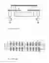
FIG. 5 is a top view showing a self-reference MRAM device comprising a plurality of the MRAM elements 1, according to an embodiment. More particularly, FIG. 5 shows the common field line 5 extending along a row of MRAM elements 1 such as to address the MRAM elements 1 along this row. The field line 5 comprises the first branch 5′ extending along the first magnetic tunnel junctions 2 and the second branch 5″ extending along the second magnetic tunnel junctions 2′. The two ends of the field line 5 are electrically connected such that when the field current 51 is passed in the field line, the first portion 51′ of the field current passes in the first branch 5′, addressing the first magnetic tunnel junctions 2, and the second portion 51″ of the field current passes in the second branch 5″, addressing the second magnetic tunnel junctions 2′. In this arrangement, the first portion 51′ of the field current can generate the first portion 52′ of magnetic field adapted to selectively vary the magnetoresistance of the first magnetic tunnel junctions 2 along the row, and the second portion 51″ of the field current can generate the second portion 52″ of magnetic field adapted to selectively vary the magnetoresistance of the second magnetic tunnel junctions 2′ along the row. In the particular arrangement of FIG. 5, the two substantially parallel branches 5′, 5″ are formed by an opening 9 provided in the common field line 5.
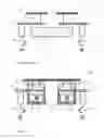
FIG. 6 represents the self-reference MRAM element 1 according to another embodiment, wherein the current line 3 is arranged substantially parallel to the first and second branches 5′, 5″.
REFERENCE NUMBERS
- 1 magnetic random access memory (MRAM) element
- 2 first magnetic tunnel junction
- 2′ second magnetic tunnel junction
- 3 current line
- 5 field line
- 5′ first branch
- 5″ second branch
- 51 field current
- 51′ first portion of field current
- 51″ second portion of field current
- 52′ first magnetic field
- 52″ second magnetic field
- 6 cladding
- 7 first strap
- 7′ second strap
- 8 first selection transistor
- 8′ second selection transistor
- 9 opening
- H magnetic field
- I current
- w width
Claims
1. Self-reference-based MRAM element comprising
a first magnetic tunnel junction and a second magnetic tunnel junction, each having a magnetoresistance that can be varied; and
a field line for passing a field current destined to vary the magnetoresistance of the first and second magnetic tunnel junctions;
the field line comprising a first branch and a second branch both branch comprises a cladding;
the first branch being arranged for passing a first portion of the field current to selectively vary the magnetoresistance of the first magnetic tunnel junction,
and the second branch being electrically connected in parallel with the first branch and arranged for passing a second portion of the field current to selectively vary the magnetoresistance of the second magnetic tunnel junction; wherein
the first and second branches each comprise cladding provided on their respective surfaces and wherein a portion of the surface of the first branch which is closest to the first magnetic tunnel junction is free of cladding so that said portion of the surface is exposed, and a portion of the surface of the second branch which is closest to the second magnetic tunnel junction is free of cladding so that said portion of the surface is exposed, so that a first portion of magnetic field generated by passing the first portion of field current in the first branch can only vary the magnetization of the first magnetic tunnel junction, and a second portion of magnetic field generated by passing the second portion of field current in the second branch can only vary the magnetization of the second magnetic tunnel junction.
2. MRAM element according to claim 1, wherein each of said first and second branches has a rectangular cross section, and wherein the cladding is comprised on three sides of the rectangular cross section.
3. MRAM element according to claim 1, wherein
the cladding comprises a ferromagnetic material.
4. MRAM element according to claim 3, wherein the ferromagnetic material comprises a NiFeCo alloy.
5. MRAM element according to claim 1,
further comprising at least one current line electrically connected to one end of each of the first and second magnetic tunnel junctions.
6. MRAM device comprising a plurality of MRAM elements, each MRAM element comprising:
a first magnetic tunnel junction and a second magnetic tunnel junction each having a magnetoresistance that can be varied; and a field line for passing a field current destined to vary the magnetoresistance of the first and second magnetic tunnel junctions; the field line comprising a first branch and a second branch both branch comprises a cladding; the first branch being arranged for passing a first portion of the field current to selectively vary the magnetoresistance of the first magnetic tunnel junction, and the second branch being electrically connected in parallel with the first branch and arranged for passing a second portion of the field current to selectively vary the magnetoresistance of the second magnetic tunnel junction; wherein the first and second branches are arranged so that a first portion of magnetic field generated by passing the first portion of field current in the first branch can only vary the magnetization of the first magnetic tunnel junction, and a second portion of magnetic field generated by passing the second portion of field current in the second branch can only vary the magnetization of the second magnetic tunnel junction.
7. MRAM device according to claim 6, wherein said plurality of the MRAM elements are arranged in rows and columns, and wherein the field line extends along a row of MRAM elements with the first branch extending along the first magnetic tunnel junctions such as to selectively vary the magnetoresistance of the first magnetic tunnel junction of the MRAM elements in the row when the first portion of the field current is passed, and with the second branch extending along the second magnetic tunnel junctions such as to selectively vary the magnetoresistance of the second magnetic tunnel junction of the MRAM elements in the row when the second portion of the field current is passed.
8. MRAM device according to claim 7, wherein the first branch is electrically connected with the second branch at each end of the row.
Images & Drawings included:
Sources:
- United States Patent and Trademark Office - verify current appl. status at the USPTO↗
Recent applications in this class:
- » 20230371275 2023-11-16
METHOD OF FORMING DIFFERENT TYPES OF MEMORY DEVICES - » 20230262992 2023-08-17
MRAM INTERCONNECT INTEGRATION WITH SUBTRACTIVE METAL PATTERNING - » 20230240080 2023-07-27
Multiferroic memory with piezoelectric layers and related methods - » 20230232637 2023-07-20
Magnetic memory device and method for forming the same - » 20230200087 2023-06-22
SEMICONDUCTOR DEVICE - » 20230200086 2023-06-22
Magneto-resistive random access memory with substitutional bottom electrode - » 20230189535 2023-06-15
Magneto-resistive random access memory with segmented bottom electrode - » 20230189534 2023-06-15
LAYERED BOTTOM ELECTRODE DIELECTRIC FOR EMBEDDED MRAM - » 20230157032 2023-05-18
BIT-LINE RESISTANCE REDUCTION - » 20230139618 2023-05-04
SEMICONDUCTOR DEVICES
Recent applications for this Assignee:
- » 20220268815 2022-08-25
Magnetic current sensor comprising a magnetoresistive differential full bridge - » 20220196764 2022-06-23
Magnetic element having an improved measurement range - » 20220050151 2022-02-17
Magnetic angular sensor device for sensing high magnetic fields with low angular error - » 20220043081 2022-02-10
Magnetoresistive-based sensing circuit for two-dimensional sensing of high magnetic fields - » 20210334482 2021-10-28
Reader device for reading information stored on a magnetic strip and a method for decoding the read information - » 20210110023 2021-04-15
MLU-based magnetic device having an authentication and physical unclonable function and authentication method using said MLU device - » 20200243127 2020-07-30
Apparatus for generating a magnetic field and method of using said apparatus - » 20200202082 2020-06-25
Magnetic reader sensor device for reading magnetic stripes and method for manufacturing the sensor device - » 20190081602 2019-03-14
Magnetoresistive-based signal shaping circuit for audio applications - » 20180336014 2018-11-22
MRAM-based programmable magnetic device for generating random numbers