Ultraviolet-erasable nonvolatile semiconductor device
US20160005744A1
2016-01-07
14/769,048
2014-01-22
✅ Patent granted
US 9,589,972 B2
2017-03-07
WO; PCT/JP2014/051182; 20140122
WO; WO2014/129252; 20140828
Theresa T Doan
Adams & Wilks
2034-01-22
Abstract:
In order to provide an ultraviolet-erasable nonvolatile semiconductor device that has a high water resistance and is capable of erasing data by ultraviolet rays, a protective film includes a silicon nitride film (12) and a silicon oxynitride film (13). The silicon nitride film (12) and the silicon oxynitride film (13) cooperate to prevent moisture from penetrating into the ultraviolet-erasable nonvolatile semiconductor device. The silicon nitride film 12 has such a thickness with which a time for erasing data in a nonvolatile semiconductor storage element (17) through irradiation of the ultraviolet rays is not increased.
Assignee:
- SII Semiconductor Corporation 70 🇯🇵 , Japan
Applicant:
Interested in similar patents?
Get notified when new applications in this technology area are published.
Classification:
H01L27/144 IPC
Devices consisting of a plurality of semiconductor or other solid-state components formed in or on a common substrate including semiconductor components sensitive to infra-red radiation, light, electromagnetic radiation of shorter wavelength or corpuscular radiation and specially adapted either for the conversion of the energy of such radiation into electrical energy or for the control of electrical energy by such radiation Devices controlled by radiation
H01L27/1443 » CPC further
Devices consisting of a plurality of semiconductor or other solid-state components formed in or on a common substrate including semiconductor components sensitive to infra-red radiation, light, electromagnetic radiation of shorter wavelength or corpuscular radiation and specially adapted either for the conversion of the energy of such radiation into electrical energy or for the control of electrical energy by such radiation; Devices controlled by radiation with at least one potential jump or surface barrier
H01L27/115 » CPC main
Devices consisting of a plurality of semiconductor or other solid-state components formed in or on a common substrate including semiconductor components specially adapted for rectifying, oscillating, amplifying or switching and having at least one potential-jump barrier or surface barrier; including integrated passive circuit elements with at least one potential-jump barrier or surface barrier the substrate being a semiconductor body including a plurality of individual components in a repetitive configuration including field-effect components; Read-only memory structures [ROM] and multistep manufacturing processes therefor Electrically programmable read-only memories; Multistep manufacturing processes therefor
H01L23/53295 » CPC further
Details of semiconductor or other solid state devices; Arrangements for conducting electric current within the device in operation from one component to another, i.e. interconnections, e.g. wires, lead frames including external interconnections consisting of a multilayer structure of conductive and insulating layers inseparably formed on the semiconductor body characterised by the materials; Insulating materials Stacked insulating layers
H01L2924/0002 » CPC further
Indexing scheme for arrangements or methods for connecting or disconnecting semiconductor or solid-state bodies as covered by; Technical content checked by a classifier Not covered by any one of groups , and
H01L23/48 IPC
Details of semiconductor or other solid state devices Arrangements for conducting electric current to or from the solid state body in operation, e.g. leads, terminal arrangements ; Selection of materials therefor
H01L23/31 IPC
Details of semiconductor or other solid state devices; Encapsulations, e.g. encapsulating layers, coatings, e.g. for protection characterised by the arrangement or shape
H01L23/532 IPC
Details of semiconductor or other solid state devices; Arrangements for conducting electric current within the device in operation from one component to another, i.e. interconnections, e.g. wires, lead frames including external interconnections consisting of a multilayer structure of conductive and insulating layers inseparably formed on the semiconductor body characterised by the materials
H01L23/3192 » CPC further
Details of semiconductor or other solid state devices; Encapsulations, e.g. encapsulating layers, coatings, e.g. for protection characterised by the arrangement or shape; Partial encapsulation or coating Multilayer coating
Description
TECHNICAL FIELD
The present invention relates to an ultraviolet-erasable nonvolatile semiconductor device.
BACKGROUND ART
Erosion by moisture has been a concern in a semiconductor device represented by a semiconductor integrated circuit. In order to cope with this, as disclosed in Patent Literature 1, a nitride film having an excellent water resistance is formed on a surface of the semiconductor device so that moisture is prevented from penetrating into the semiconductor device, to thereby enhance a water resistance of the semiconductor device.
CITATION LIST
Patent Literature
[PTL 1] JP 2006-344956 A
SUMMARY OF INVENTION
Technical Problem
However, when the technology disclosed in Patent Literature 1 is applied to an ultraviolet-erasable nonvolatile semiconductor device capable of erasing data by ultraviolet rays, due to the presence of the nitride film, the water resistance of the semiconductor device is enhanced but the ultraviolet rays are difficult to transmit therethrough, and hence the data cannot be erased by the ultraviolet rays or a large amount of time is required to erase the data. Thus, a structure has been demand that has a high water resistance and is suitable for an ultraviolet-erasable nonvolatile semiconductor device capable of erasing data by ultraviolet rays.
The present invention has been made in view of the problems described above, and provides an ultraviolet-erasable nonvolatile semiconductor device that has a high water resistance and is capable of erasing data by ultraviolet rays.
Solution to Problem
In order to solve the problems described above, according to one embodiment of the present invention, there is provided an ultraviolet-erasable nonvolatile semiconductor device, including: a semiconductor substrate; a nonvolatile semiconductor storage element formed in the semiconductor substrate; a top metal formed on the semiconductor substrate; and a protective film formed on the top metal. The protective film includes a silicon nitride film and a silicon oxynitride film. The silicon nitride film and the silicon oxynitride film cooperate to prevent moisture from penetrating into the ultraviolet-erasable nonvolatile semiconductor device. The silicon nitride film has such a thickness with which it is possible to shorten a time for erasing data in the nonvolatile semiconductor storage element through irradiation of ultraviolet rays.
Advantageous Effects of Invention
The ultraviolet-erasable nonvolatile semiconductor device according to the one embodiment of the present invention has the high water resistance and is capable of erasing the data by the ultraviolet rays.
BRIEF DESCRIPTION OF DRAWINGS
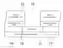
FIG. 1 is a sectional view of an ultraviolet-erasable nonvolatile semiconductor device.
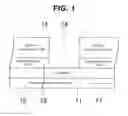
FIG. 2 is a sectional view of an ultraviolet-erasable nonvolatile semiconductor device.
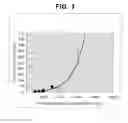
FIG. 3 is a graph for showing a relationship between a thickness of a silicon nitride film and a time for erasing data in an ultraviolet-erasable nonvolatile semiconductor storage element.
DESCRIPTION OF EMBODIMENTS
In the following, embodiments of the present invention are described with reference to the drawings.
An ultraviolet-erasable nonvolatile semiconductor device is now described. FIG. 1 is a sectional view of the ultraviolet-erasable nonvolatile semiconductor device. FIG. 3 is a graph for showing a relationship between a thickness of a silicon nitride film and a time for erasing data in an ultraviolet-erasable nonvolatile semiconductor storage element.
The ultraviolet-erasable nonvolatile semiconductor device includes a semiconductor substrate 10, a nonvolatile semiconductor storage element 17 formed in the semiconductor substrate 10, a top metal 11 formed on the semiconductor substrate 10, and a protective film formed on the top metal 11. Further, the ultraviolet-erasable nonvolatile semiconductor device includes, in part thereof, a pad opening portion 14 obtained by removing the protective film formed on the top metal 11. In this case, the protective film includes two layers of a silicon nitride film 12 and a silicon oxynitride film 13.
Part of the top metal 11 is exposed from the pad opening portion 14, and necessary signal transmission is performed therewith. The silicon nitride film 12 and the silicon oxynitride film 13 cooperate to prevent moisture from penetrating into the ultraviolet-erasable nonvolatile semiconductor device. As a thickness of the silicon nitride film 12 is increased, ultraviolet rays are more difficult to transmit therethrough, and hence such a thickness is selected with which it is possible to shorten the time for erasing data in the nonvolatile semiconductor storage element 17 through irradiation of the ultraviolet rays.
Through a publicly-known semiconductor manufacturing process, the nonvolatile semiconductor storage element 17 such as an erasable programmable read only memory (EPROM) is formed in the semiconductor substrate 10. After that, an inter-layer insulating film (not shown) and the like are laminated on the resultant, and then the top metal 11 is laminated thereon. After that, as the protective film, the silicon nitride film 12 and then the silicon oxynitride film 13 are laminated thereon. After that, the pad opening portion 14 is formed in part of the protective film formed on the top metal 11.
In this case, the silicon nitride film 12 is formed so as to have a thickness of about 1,000 Å or more in order to ensure the water resistance. Moreover, as shown in FIG. 3, when the thickness of the silicon nitride film 12 exceeds about 2,000 Å, the time for erasing data in the ultraviolet-erasable nonvolatile semiconductor storage element is precipitously increased. Thus, it is required that the thickness of the silicon nitride film 12 be set to be about 2,000 Å or less so that the time for erasing data is not unnecessarily increased. With this, the data in the nonvolatile semiconductor storage element 17 can be erased by the ultraviolet rays even in the manufacturing process.
Moreover, the silicon oxynitride film 13 is formed so as to have a refractive index of from 1.65 to 1.85 and a thickness of about 7,000 Å or more, and hence the water resistance can be enhanced. Note that, the silicon oxynitride film 13 does not inhibit the entrance of the ultraviolet rays.
With the configuration described above, the ultraviolet-erasable nonvolatile semiconductor device can have the high water resistance and erase the data by the ultraviolet rays within a period of time that allows the mass production.
Note that, in FIG. 1, the silicon oxynitride film 13 is laminated on the silicon nitride film 12. Although not illustrated, the silicon nitride film 12 may be laminated on the silicon oxynitride film 13.
Moreover, as illustrated in FIG. 2, a TEOS film 15 may be added as the protective film between the silicon nitride film and the silicon oxynitride film.
REFERENCE SIGNS LIST
10 semiconductor substrate
11 top metal
12 silicon nitride film
13 silicon oxynitride film
14 pad opening portion
15 TEOS film
17 nonvolatile semiconductor storage element
Claims
1. An ultraviolet-erasable nonvolatile semiconductor device, comprising:
a semiconductor substrate;
an ultraviolet-erasable nonvolatile semiconductor storage element formed in a surface of the semiconductor substrate;
a top metal formed on the semiconductor substrate; and
a protective film formed on the ultraviolet-erasable nonvolatile semiconductor storage element and the top metal, the protective film comprising a silicon nitride film and a silicon oxynitride film laminated thereon.
2. An ultraviolet-erasable nonvolatile semiconductor device according to claim 1, wherein the silicon nitride film has a thickness of 1,000 Å or more and 2,000 Å or less.
3. An ultraviolet-erasable nonvolatile semiconductor device according to claim 1, wherein the silicon oxynitride film has a refractive index of from 1.65 to 1.85.
4. An ultraviolet-erasable nonvolatile semiconductor device according to claim 1, further comprising a TEOS film formed between the silicon nitride film and the silicon oxynitride film.
Images & Drawings included:
Sources:
- United States Patent and Trademark Office - verify current appl. status at the USPTO↗
Recent applications in this class:
- » 20230133927 2023-05-04
Technologies for fabricating a 3D memory structure - » 20220359539 2022-11-10
MICROELECTRONIC DEVICES WITH TIER STACKS WITH VARIED TIER THICKNESSES, AND RELATED METHODS AND SYSTEMS - » 20220302133 2022-09-22
3D vertical nand memory device including multiple select lines and control lines having different vertical spacing - » 20220238535 2022-07-28
Three-dimensional semiconductor device - » 20220181333 2022-06-09
Semiconductor storage device and method for producing semiconductor storage device - » 20220149052 2022-05-12
Three-dimensional memory device having parallel trench type capacitor - » 20220028870 2022-01-27
Atomic layer deposition of III-V compounds to form V-NAND devices - » 20220013529 2022-01-13
Storage device - » 20210398988 2021-12-23
Semiconductor device - » 20210398987 2021-12-23
Microelectronic devices with tier stacks with varied tier thicknesses, and related methods and systems
Recent applications for this Assignee:
- » 20170351180 2017-12-07
Reticle transmittance measurement method, projection exposure method using the same, and projection exposure device - » 20170263521 2017-09-14
Resin-encapsulated semiconductor device - » 20170257028 2017-09-07
Switching regulator for detecting a plurality of abnormalities using only one comparison circuit - » 20170256582 2017-09-07
Semiconductor device and a method of manufacturing a semiconductor device - » 20170256545 2017-09-07
Method of manufacturing semiconductor integrated circuit device - » 20170162588 2017-06-08
Semiconductor nonvolatile memory element - » 20170025320 2017-01-26
Resin-encapsulatd semiconductor device and method of manufacturing the same - » 20170005174 2017-01-05
Method of manufacturing a semiconductor device - » 20160351731 2016-12-01
Optical sensor device - » 20160351730 2016-12-01
Optical sensor device