FOUR-PHASE CHARGE PUMP CIRCUIT
US20160006349A1
2016-01-07
14/520,355
2014-10-22
Abstract:
A four-phase charge pump circuit including an output stage and multiple boosting stages is provided. The multiple boosting stages are coupled to the output stage in series, and each of the multiple boosting stages is driven by four-phase clock signals. The output stage is driven by two clock signals of the four-phase clock signals and outputs a positive boosted voltage, and thereby the four-phase charge pump circuit is a positive charge pump circuit. Each of the boosting stages includes two branch charge pumps, and each of the two branch charge pumps includes a main pass transistor and a pre-charge transistor. The main pass transistors and the pre-charge transistors of the boosting stages are disposed on an identical deep doped region.
Interested in similar patents?
Get notified when new applications in this technology area are published.
Classification:
H02M3/07 » CPC main
Conversion of dc power input into dc power output without intermediate conversion into ac by static converters using resistors or capacitors, e.g. potential divider using capacitors charged and discharged alternately by semiconductor devices with control electrode, e.g. charge pumps
H03K17/687 » CPC further
Electronic switching or gating, i.e. not by contact-making and –breaking characterised by the components used by the use, as active elements, of semiconductor devices the devices being field-effect transistors
Description
CROSS-REFERENCE TO RELATED APPLICATION
This application claims the priority benefits of U.S. provisional application Ser. No. 62/021,216, filed on Jul. 7, 2014. The entirety of the above-mentioned patent application is hereby incorporated by reference herein and made a part of this specification.
BACKGROUND
1. Technical Field
The disclosure relates to a charge pump circuit. Particularly, the disclosure relates to a four-phase charge pump circuit.
2. Related Art
In order to lower power consumption, an operating voltage for integrated circuits (ICs) is modified to a lower level. For example, the normal operating voltage for the ICs has been changed from the early 5 volts to the present 3.3 volts, and sometimes even lower than 2 volts. Although a lower operating voltage is beneficial for power consumption reduction, some particular applications requiring a high operating voltage still should be concerned. In particular, while erasing data stored in a flash memory, a high voltage, is necessary and supplied by a charge pump circuit.
Generally, a charge pump circuit supplying positive voltage is composed of P-channel metal-oxide-semiconductor (PMOS) transistors. On the contrary, a charge pump circuit supplying negative voltage could be composed of NMOS transistors. However, PMOS transistors have weaker driving capability and lower transconductance than NMOS transistors such that a PMOS type charge pump circuit is less efficient or occupies relatively larger area than a NMOS type charge pump circuit in certain operation conditions.
SUMMARY
The disclosure is directed to a four-phase charge pump circuit, which occupies relatively small chip area.
The disclosure provides a four-phase charge pump circuit including multiple boosting stages. The boosting stages are driven by four-phase clock signals. Each of the boosting stages includes two branch charge pumps, and each of the two branch charge pumps includes a main pass transistor and a pre-charge transistor. The main pass transistor has a body, a gate terminal, a source terminal as a first node of the branch charge pump and a drain terminal as a second node of the branch charge pump. The first node and the second node of the branch charge pump connect respectively to a front boosting stage and a rear boosting stage of the boosting stages. The pre-charge transistor has a gate terminal, a source terminal and a drain terminal. The source terminal and the drain terminal of the pre-charge transistor are respectively coupled to the gate terminal of the main transistor and the first node of the branch charge pump. The gate terminal of the pre-charge transistor is coupled to the second node of the branch charge pump. The main pass transistors and the pre-charge transistors of the boosting stages are disposed on an identical deep doped region.
In an embodiment of the disclosure, each of the two branch charge pumps further includes two capacitors. The two capacitors are coupled respectively to the gate terminal of the main pass transistor and the second node of the branch charge pump.
In an embodiment of the disclosure, for each of the boosting stages, the two capacitors of one branch charge pump receive two clock signals of the four-phase clock signals, and the two capacitors of the other branch charge pump receive the other two clock signals of the four-phase clock signals.
In an embodiment of the disclosure, each of the two branch charge pumps further includes two substrate transistors. Each of the two substrate transistors has a body, a gate terminal, a source terminal and a drain terminal. The source terminals and the bodies of the two substrate transistors are connected together to the body of the main pass transistor. The drain terminals of the two substrate transistors are connected respectively to the first node and the second node of the branch charge pump. The gate terminal of one substrate transistor, whose drain terminal connects to the second node, is connected to the first node of one branch charge pump that the one substrate transistor is located, and the gate terminal of the other substrate transistor is connected to the first node of the other branch charge pump.
In an embodiment of the disclosure, each of the two branch charge pumps further includes an initial transistor. The initial transistor has a body, a gate terminal, a source terminal and a drain terminal. The drain terminal and the source terminal of the initial transistor are respectively coupled to the first node and the second node of the branch charge pump. The gate terminal of the initial transistor is coupled to the drain terminal of the initial transistor, and the body of the initial transistor are connected to the body of the main pass transistor.
In an embodiment of the disclosure, potential at the body of each of the main pass transistors and the initial transistors of the boosting stages is kept at a lower substrate level.
In an embodiment of the disclosure, the substrate transistors and the initial transistors of the boosting stages are disposed on the identical deep doped region.
In an embodiment of the disclosure, the main pass transistors, the pre-charge transistors, the substrate transistors and the initial transistors of the boosting stages are N-channel metal-oxide-semiconductor field-effect transistors (MOSFETs).
In an embodiment of the disclosure, the four-phase charge pump circuit further includes an output stage. The output stage is driven by two clock signals of the four-phase clock signals and outputs a boosted voltage. The multiple boosting stages are coupled to the output stage.
In an embodiment of the disclosure, the output stage includes two branch output circuits, and each of the two branch output circuits includes a main pass transistor and a pre-charge transistor. The main pass transistor has a body, a gate terminal, a source terminal as a first node of the branch output circuit and a drain terminal as a second node of the branch output circuit. The first node of the branch output circuit connects to a front boosting stage of the boosting stages, and the second node of the branch output circuit serves as an output end of the output stage to output the boosted voltage. The pre-charge transistor has a gate terminal, a source terminal and a drain terminal. The source terminal and the drain terminal of the pre-charge transistor are respectively coupled to the gate terminal of the main transistor and the first node of the branch output circuit, and the gate terminal of the pre-charge transistor is coupled to the second node of the branch output circuit. The main pass transistors and the pre-charge transistors of the output stage are disposed on the identical deep doped region.
In an embodiment of the disclosure, each of the two branch output circuits further includes one capacitor. The one capacitor is coupled to the gate terminal of the main pass transistor. The capacitors of the output stage receive two clock signals of the four-phase clock signals.
In an embodiment of the disclosure, each of the two branch charge pumps further includes two substrate transistors. Each of The two substrate transistors has a body, a gate terminal, a source terminal and a drain terminal. The source terminals and the bodies of the two substrate transistors are connected together to the body of the main pass transistor. The drain terminals of the two substrate transistors are connected respectively to the first node and the second node of the branch output circuit. The gate terminal of one substrate transistor, whose drain terminal connects to the second node, is connected to the first node of one branch output circuit that the one substrate transistor is located, and the gate terminal of the other substrate transistor is connected to the first node of the other branch output circuit.
In an embodiment of the disclosure, potential at the body of each of the main pass transistors of the output stage is kept at a lower substrate level.
In an embodiment of the disclosure, the substrate transistors of the output stage are disposed on the identical deep doped region.
In an embodiment of the disclosure, the main pass transistors, the pre-charge transistors and the substrate transistors of the output stage are N-channel MOSFETs.
In an embodiment of the disclosure, the four-phase charge pump circuit is a positive charge pump circuit.
According to the above descriptions, the transistors of the multiple boosting stages in the disclosure are disposed on the same deep doped region, and thereby the occupied chip area may be reduced and smaller than that of the charge pump circuit whose deep doped region are separated for each boosting stage.
In order to make the aforementioned and other features and advantages of the disclosure comprehensible, several exemplary embodiments accompanied with figures are described in detail below.
BRIEF DESCRIPTION OF THE DRAWINGS
The accompanying drawings are included to provide a further understanding of the disclosure, and are incorporated in and constitute a part of this specification. The drawings illustrate embodiments of the disclosure and, together with the description, serve to explain the principles of the disclosure.
FIG. 1 is a schematic diagram of a four-phase charge pump circuit according to an embodiment of the disclosure.
FIG. 2A shows waveforms of four-phase clock signals applied for the circuit of FIG. 1 in accordance with an embodiment of the disclosure.
FIG. 2B shows waveforms of four-phase clock signals applied for the circuit of FIG. 1 in accordance with another embodiment of the disclosure.
FIG. 3 illustrates an internal circuit structure of the odd-numbered voltage boosting stage according to the embodiment of FIG. 1.
FIG. 4 illustrates an internal circuit structure of the even-numbered voltage boosting stage according to the embodiment of FIG. 1.
FIG. 5 illustrates an internal circuit structure of the output stage according to the embodiment of FIG. 1.
FIG. 6 illustrates a schematic structure drawing of the multiple boosting stages according to an exemplary embodiment of the disclosure.
FIG. 7 illustrates a schematic circuit diagram of each transistor of the boosting stages.
FIG. 8 is a schematic diagram of a four-phase charge pump circuit according to another embodiment of the disclosure.
DETAILED DESCRIPTION OF DISCLOSED EMBODIMENTS
The term “coupling/coupled” used in this specification (including claims) may refer to any direct or indirect connection means. For example, “a first device is coupled to a second device” should be interpreted as “the first device is directly connected to the second device” or “the first device is indirectly connected to the second device through other devices or connection means.” Moreover, wherever appropriate in the drawings and embodiments, elements/components/steps with the same reference numerals represent the same or similar parts. Elements/components/steps with the same reference numerals or names in different embodiments may be cross-referenced. A plurality of embodiments are provided below to describe the disclosure in detail, though the disclosure is not limited to the provided embodiments, and the provided embodiments can be suitably combined.
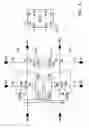
FIG. 1 is a schematic diagram of a four-phase charge pump circuit according to an embodiment of the disclosure. FIG. 2A shows waveforms of four-phase clock signals applied for the circuit of FIG. 1 in accordance with an embodiment of the disclosure. With reference to FIG. 1 and FIG. 2A, a four-phase charge pump circuit 100 in accordance with the disclosure includes an output stage 110 and multiple boosting stages 120_1 to 120_N, where N is a positive integer larger than 1. The multiple boosting stages 120_1 to 120_N are coupled to the output stage 110 in series, and each of the multiple boosting stages 120_1 to 120_N is driven by the four-phase clock signals P11, P22, P33 and P44 as shown in FIG. 2A. The output stage 110 is driven by the four-phase clock signals P22 and P44 and outputs a positive boosted voltage VPP, and thereby the four-phase charge pump circuit 100 is a positive charge pump circuit.
In the embodiment as exemplarily disclosed in FIG. 1, the four-phase charge pump circuit 100 may include even-numbered boosting stages 120_1 to 120_N, i.e., N is an even number larger than 1. The boosting stage 120_1 receives an input voltage VDD, and the input voltage VDD is sequentially boosted by the multiple boosting stages 120_1 to 120_N stage by stage, and then the boosting stage 120_N outputs middle boosted voltages UN and DN to the output stage 110. In this case, the middle boosted voltages UN and DN outputted to the output stage 110 may be N+1 times larger than the input voltage VDD, e.g., UN=(N+1) VDD. The output stage 110 receives the middle boosted voltages UN and DN and enhances the driving capability of the middle boosted voltages UN and DN to thereby generate the positive boosted voltage VPP.
It should be noted that, an amount of the multiple boosting stages 120_1 to 120_N included in the four-phase charge pump circuit 100 in the present embodiment may be adjusted according to different actual circuit design, which are not particularly limited by the disclosure. In other exemplary embodiments, the four-phase charge pump circuit 100 may include odd-numbered boosting stages 120_1 to 120_N, i.e., N is an odd number larger than 1. In this case, the output stage 110 may be driven in another manner. The upper branch output circuit inside the output stage 110 may be driven by the clock signal P22, and the lower branch output circuit inside the output stage 110 may be driven by the clock signal P44.
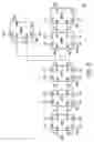
FIG. 3 illustrates an internal circuit structure of the odd-numbered voltage boosting stage according to the embodiment of FIG. 1. Referring to FIG. 3, the internal circuit structure of the voltage boosting stage 120_1, 120_3 . . . or 120_(N−1) (not shown in FIG. 1) is illustrated in FIG. 3. The voltage boosting stage 120_1 is taken as an example in the following description, and the other voltage boosting stage 120_3 . . . and 120_(N−1) can be deduced by analogy.
In the present embodiment, the voltage boosting stage 120_1 includes an upper branch charge pump 121 and a lower branch charge pump 123. The upper branch charge pump 121 includes a main pass transistor NO, a pre-charge transistor N3, two capacitors C1 and C2, two substrate transistors N1 and N2 and an initial transistor N6. The source terminal of the main pass transistor NO serves as a first node U0 of the upper branch charge pump 121, and the drain terminal of the main pass transistor N0 serves as a second node U1 of the upper branch charge pump 121. In this embodiment, the voltage boosting stage 120_1 is the first voltage boosting stage of the boosting stages 120_1 to 120_N and thereby configured to receive the input voltage VDD via the input pads IN1 and IN2. The first node U0 of the upper branch charge pump 121 receives the input voltage VDD via the input pad IN1. The second node U1 of the upper branch charge pump 121 connect to the rear boosting stage 120_2 via the output pad OUT1. The source terminal and the drain terminal of the pre-charge transistor N3 are respectively coupled to the gate terminal of the main transistor NO and the first node U0 of the upper branch charge pump 121, and the gate terminal of the pre-charge transistor N3 is coupled to the second node U1 of the upper branch charge pump 121. The body of the pre-charge transistor N3 are connected to the body BU of the main pass transistor NO. One terminal of the capacitor C2 is coupled to the gate terminal of the main pass transistor NO, and the other terminal of the capacitor C2 receives the clock signal P44. One terminal of the capacitor C1 is coupled to the second node U1 of the upper branch charge pump 121, and the other terminal of the capacitor C1 receives the clock signal P11. The source terminals and the bodies of the two substrate transistors N1 and N2 are connected together to the body BU of the main pass transistor NO, and the drain terminals of the two substrate transistors N1 and N2 are connected respectively to the first node U0 and the second node U1 of the upper branch charge pump 121. The gate terminal of the substrate transistor N2 is connected to the first node U0 of the upper branch charge pump 121, and the gate terminal of the substrate transistor N1 is connected to the first node D0 of the lower branch charge pump 123. That is to say, in the upper branch charge pump 121 of the present embodiment, the gate terminal of one substrate transistor N2, whose drain terminal connects to the second node U1, is connected to the first node U0 of one branch charge pump 121 that the one substrate transistor N2 is located, and the gate terminal of the other substrate transistor N1 is connected to the first node D0 of the other branch charge pump 123. The substrate transistors N1 and N2 are switched to keep potential at the body BU of the main pass transistor N0 at a lower substrate level to mitigate the body effect. The drain terminal and the source terminal of the initial transistor N6 are respectively coupled to the first node and the second node of the upper branch charge pump 121, i.e., the input pad IN1 and the output pad OUT1. The gate terminal of the initial transistor N6 is coupled to the drain terminal itself, and the body of the initial transistor N6 are connected to the body BU of the main pass transistor N0.
Similarly, the lower branch charge pump 123 also includes a main pass transistor N7, a pre-charge transistor N10, two capacitors C3 and C4, two substrate transistors N8 and N9 and an initial transistor N13. The source terminal of the main pass transistor N7 serves as a first node D0 of the lower branch charge pump 123, and the drain terminal of the main pass transistor N7 serves as a second node D1 of the lower branch charge pump 123. In this embodiment, the first node D0 of the lower branch charge pump 123 receives the input voltage VDD via the input pad IN2. The second node D1 of the lower branch charge pump 123 connect to the rear boosting stage 120_2 via the output pad OUT2. The source terminal and the drain terminal of the pre-charge transistor N10 are respectively coupled to the gate terminal of the main transistor N7 and the first node D0 of the lower branch charge pump 123, and the gate terminal of the pre-charge transistor N10 is coupled to the second node D1 of the lower branch charge pump 123. The body of the pre-charge transistor N10 are connected to the body BD of the main pass transistor N7. One terminal of the capacitor C4 is coupled to the gate terminal of the main pass transistor N7, and the other terminal of the capacitor C4 receives the clock signal P22. One terminal of the capacitor C3 is coupled to the second node D1 of the lower branch charge pump 123, and the other terminal of the capacitor C3 receives the clock signal P33. The source terminals and the bodies of the two substrate transistors N8 and N9 are connected together to the body BD of the main pass transistor N7, and the drain terminals of the two substrate transistors N8 and N9 are connected respectively to the first node D0 and the second node D1 of the lower branch charge pump 123. The gate terminal of the substrate transistor N9 is connected to the first node D0 of the lower branch charge pump 123, and the gate terminal of the substrate transistor N8 is connected to the first node U0 of the upper branch charge pump 121. That is to say, in the lower branch charge pump 123 of the present embodiment, the gate terminal of one substrate transistor N9, whose drain terminal connects to the second node D1, is connected to the first node D0 of one branch charge pump 123 that the one substrate transistor N9 is located, and the gate terminal of the other substrate transistor N8 is connected to the first node U0 of the other branch charge pump 121. The substrate transistors N8 and N9 are switched to keep potential at the body BD of the main pass transistor N7 at a lower substrate level to mitigate the body effect. The drain terminal and the source terminal of the initial transistor N13 are respectively coupled to the first node and the second node of the lower branch charge pump 123, i.e., the input pad IN2 and the output pad OUT2. The gate terminal of the initial transistor N13 is coupled to the drain terminal itself, and the body of the initial transistor N13 are connected to the body BD of the main pass transistor N7.
FIG. 4 illustrates an internal circuit structure of the even-numbered voltage boosting stage according to the embodiment of FIG. 1. Referring to FIG. 4, the internal circuit structure of the voltage boosting stage 120_2, 120_4 (not shown in FIG. 1) . . . or 120_N is illustrated in FIG. 4. The voltage boosting stage 120_2 is taken as an example in the following description, and the other voltage boosting stage 120_4 . . . and 120_N can be deduced by analogy.
In the present embodiment, the voltage boosting stage 120_2 includes an upper branch charge pump 122 and a lower branch charge pump 124. The upper branch charge pump 122 includes a main pass transistor NO, a pre-charge transistor N3, two capacitors C1 and C2, two substrate transistors N1 and N2 and an initial transistor N6. The source terminal of the main pass transistor NO serves as a first node U1 of the upper branch charge pump 122, and the drain terminal of the main pass transistor NO serves as a second node U2 of the upper branch charge pump 122. In this embodiment, the first node U1 of the upper branch charge pump 122 connect to the front boosting stage 120_1 via the input pad IN1. The second node U2 of the upper branch charge pump 122 connect to the rear boosting stage 120_3 via the output pad OUT1. In FIG. 1, the voltage boosting stage 120_N is the last voltage boosting stage of the boosting stages 120_1 to 120_N and thereby configured to respectively output the middle boosted voltages UN and DN via the output pads OUT1 and OUT2. The source terminal and the drain terminal of the pre-charge transistor N3 are respectively coupled to the gate terminal of the main transistor NO and the first node U1 of the upper branch charge pump 122, and the gate terminal of the pre-charge transistor N3 is coupled to the second node U2 of the upper branch charge pump 122. The body of the pre-charge transistor N3 are connected to the body BU of the main pass transistor N0. One terminal of the capacitor C2 is coupled to the gate terminal of the main pass transistor N0, and the other terminal of the capacitor C2 receives the clock signal P22. One terminal of the capacitor C1 is coupled to the second node U2 of the upper branch charge pump 122, and the other terminal of the capacitor C1 receives the clock signal P33. The source terminals and the bodies of the two substrate transistors N1 and N2 are connected together to the body BU of the main pass transistor NO, and the drain terminals of the two substrate transistors N1 and N2 are connected respectively to the first node U1 and the second node U2 of the upper branch charge pump 122. The gate terminal of the substrate transistor N2 is connected to the first node U1 of the upper branch charge pump 122, and the gate terminal of the substrate transistor N1 is connected to the first node D1 of the lower branch charge pump 124. That is to say, in the upper branch charge pump 122 of the present embodiment, the gate terminal of one substrate transistor N2, whose drain terminal connects to the second node U2, is connected to the first node U1 of one branch charge pump 122 that the one substrate transistor N2 is located, and the gate terminal of the other substrate transistor N1 is connected to the first node D1 of the other branch charge pump 124. The substrate transistors N1 and N2 are switched to keep potential at the body BU of the main pass transistor NO at a lower substrate level to mitigate the body effect. The drain terminal and the source terminal of the initial transistor N6 are respectively coupled to the first node and the second node, i.e., the input pad IN1 and the output pad OUT1. The gate terminal of the initial transistor N6 is coupled to the drain terminal itself, and the body of the initial transistor N6 are connected to the body BU of the main pass transistor NO.
Similarly, the lower branch charge pump 124 also includes a main pass transistor N7, a pre-charge transistor N10, two capacitors C3 and C4, two substrate transistors N8 and N9 and an initial transistor N13. The source terminal of the main pass transistor N7 serves as a first node D1 of the lower branch charge pump 124, and the drain terminal of the main pass transistor N7 serves as a second node D2 of the lower branch charge pump 124. In this embodiment, the first node D1 of the lower branch charge pump 124 connect to the front boosting stage 120_1 via the input pad IN2. The second node D2 of the lower branch charge pump 124 connect to the rear boosting stage 1203 via the output pad OUT2. The source terminal and the drain terminal of the pre-charge transistor N10 are respectively coupled to the gate terminal of the main transistor N7 and the first node D1 of the lower branch charge pump 124, and the gate terminal of the pre-charge transistor N10 is coupled to the second node D2 of the lower branch charge pump 124. The body of the pre-charge transistor N10 are connected to the body BD of the main pass transistor N7. One terminal of the capacitor C4 is coupled to the gate terminal of the main pass transistor N7, and the other terminal of the capacitor C4 receives the clock signal P44. One terminal of the capacitor C3 is coupled to the second node D2 of the lower branch charge pump 124, and the other terminal of the capacitor C3 receives the clock signal P11. The source terminals and the bodies of the two substrate transistors N8 and N9 are connected together to the body BD of the main pass transistor N7, and the drain terminals of the two substrate transistors N8 and N9 are connected respectively to the first node D1 and the second node D2 of the lower branch charge pump 124. The gate terminal of the substrate transistor N9 is connected to the first node D1 of the lower branch charge pump 124, and the gate terminal of the substrate transistor N8 is connected to the first node U1 of the upper branch charge pump 122. That is to say, in the lower branch charge pump 124 of the present embodiment, the gate terminal of one substrate transistor N9, whose drain terminal connects to the second node D2, is connected to the first node D1 of one branch charge pump 124 that the one substrate transistor N9 is located, and the gate terminal of the other substrate transistor N8 is connected to the first node U1 of the other branch charge pump 122. The substrate transistors N8 and N9 are switched to keep potential at the body BD of the main pass transistor N7 at a lower substrate level to mitigate the body effect. The drain terminal and the source terminal of the initial transistor N13 are respectively coupled to the first node and the second node of the lower branch charge pump 124, i.e., the input pad IN2 and the output pad OUT2. The gate terminal of the initial transistor N13 is coupled to the drain terminal itself, and the body of the initial transistor N13 are connected to the body BD of the main pass transistor N7.
In the embodiments as exemplarily disclosed in FIG. 1, FIG. 3 and FIG. 4, the main pass transistors NO and N7, the pre-charge transistors N3 and N10, the substrate transistors N1, N2, N8 and N9 and the initial transistors N6 and N13 of the boosting stages 120_1 to 120_N are N-channel metal-oxide-semiconductor field-effect transistors (MOSFETs).
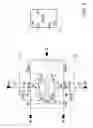
FIG. 5 illustrates an internal circuit structure of the output stage according to the embodiment of FIG. 1.
In the present embodiment, the output stage 110 includes an upper branch output circuit 111 and a lower branch output circuit 113. The upper branch output circuit 111 includes a main pass transistor NO, a pre-charge transistor N3, one capacitor C2, two substrate transistors N1 and N2. The source terminal of the main pass transistor NO serves as a first node UN of the upper branch output circuit 111, and the drain terminal of the main pass transistor NO serves as a second node U(N+1) of the upper branch output circuit 111. In this embodiment, the first node UN of the upper branch output circuit 111 connect to the front boosting stage 120_N via the input pad IN1. The second node U(N+1) of the upper branch output circuit 111 outputs the boosted voltage VPP via an output pad OUT. The source terminal and the drain terminal of the pre-charge transistor N3 are respectively coupled to the gate terminal of the main transistor NO and the first node UN of the upper branch output circuit 111, and the gate terminal of the pre-charge transistor N3 is coupled to the second node U(N+1) of the upper branch output circuit 111. The body of the pre-charge transistor N3 are connected to the body BU of the main pass transistor NO. One terminal of the capacitor C2 is coupled to the gate terminal of the main pass transistor N0, and the other terminal of the capacitor C2 receives the clock signal P44. The source terminals and the bodies of the two substrate transistors N1 and N2 are connected together to the body BU of the main pass transistor NO, and the drain terminals of the two substrate transistors N1 and N2 are connected respectively to the first node UN and the second node U(N+1) of the upper branch output circuit 111. The gate terminal of the substrate transistor N2 is connected to the first node UN of the upper branch output circuit 111, and the gate terminal of the substrate transistor N1 is connected to the first node DN of the lower branch output circuit 113. That is to say, in the upper branch output circuit 111 of the present embodiment, the gate terminal of one substrate transistor N2, whose drain terminal connects to the second node U(N+1), is connected to the first node UN of one branch output circuit 111 that the one substrate transistor N2 is located, and the gate terminal of the other substrate transistor N1 is connected to the first node DN of the other branch output circuit 113. The substrate transistors N1 and N2 are switched to keep potential at the body BU of the main pass transistor NO at a lower substrate level to mitigate the body effect.
Similarly, the lower branch output circuit 113 also includes a main pass transistor N7, a pre-charge transistor N10, one capacitor C4, two substrate transistors N8 and N9 and an initial transistor N13. The source terminal of the main pass transistor N7 serves as a first node DN of the lower branch output circuit 113, and the drain terminal of the main pass transistor N7 serves as a second node D(N+1) of the lower branch output circuit 113. In this embodiment, the first node DN of the lower branch output circuit 113 connect to the front boosting stage 120_N via the input pad IN2. The second node D(N+1) of the lower branch output circuit 113 outputs the boosted voltage VPP via the same output pad as that of the upper branch output circuit 111. The source terminal and the drain terminal of the pre-charge transistor N10 are respectively coupled to the gate terminal of the main transistor N7 and the first node DN of the lower branch output circuit 113, and the gate terminal of the pre-charge transistor N10 is coupled to the second node D(N+1) of the lower branch output circuit 113. The body of the pre-charge transistor N10 are connected to the body BD of the main pass transistor N7. One terminal of the capacitor C4 is coupled to the gate terminal of the main pass transistor N7, and the other terminal of the capacitor C4 receives the clock signal P22. The source terminals and the bodies of the two substrate transistors N8 and N9 are connected together to the body BD of the main pass transistor N7, and the drain terminals of the two substrate transistors N8 and N9 are connected respectively to the first node DN and the second node D(N+1) of the lower branch output circuit 113. The gate terminal of the substrate transistor N9 is connected to the first node DN of the lower branch output circuit 113, and the gate terminal of the substrate transistor N8 is connected to the first node UN of the upper branch output circuit 111. That is to say, in the lower branch output circuit 113 of the present embodiment, the gate terminal of one substrate transistor N9, whose drain terminal connects to the second node D(N+1), is connected to the first node DN of one branch output circuit 113 that the one substrate transistor N9 is located, and the gate terminal of the other substrate transistor N8 is connected to the first node UN of the other branch output circuit 111. The substrate transistors N8 and N9 are switched to keep potential at the body BD of the main pass transistor N7 at a lower substrate level to mitigate the body effect.
In the embodiment as exemplarily disclosed in FIG. 5, the main pass transistors NO and N7, the pre-charge transistors N3 and N10 and the substrate transistors N1, N2, N8 and N9 of the output stage 110 are N-channel MOSFETs. The boosted voltage VPP is a positive voltage, and thereby the four-phase charge pump circuit 100 is a positive charge pump circuit.
With reference to FIG. 2A to FIG. 4, the upper branch charge pumps 121 and 122 and the lower branch charge pumps 123 and 124 are driven by the four clock signals P11, P22, P33 and P44 as shown in FIG. 2A, so as to perform a voltage boosting operation stage by stage. The main pass transistors NO and N7 in accompaniment with the substrate transistors N1, N2, N8 and N9 perform a bias switching operation to keep the bias of the main pass transistors NO and N7 at a lower substrate level thus mitigating the body effect.
FIG. 2A shows waveforms of four-phase clock signals applied for the circuit of FIG. 1 in accordance with an embodiment of the disclosure. In the following description, the operation of the first boosting stage 120_1 is divided into several time periods P1 to P3. The operations of the boosting stages 120_3 . . . and 120_(N−1) (not shown in FIG. 1) can be deduced by analogy.
Referring to FIG. 2A to FIG. 3, during the first time period P1, the clock signals P33 and P44 are at high levels, and the clock signals P11 and P22 are at low levels. In the upper branch charge pump 121, the main pass transistors NO is turned on, and the input voltage VDD is transmitted from the first node U0 to the second node U1. In the lower branch charge pump 123, the pre-charge transistor N10 is turned on to pre-charge the gate terminal GD0 of the main pass transistors N7 by using the input voltage VDD and reduce the reverse current of the main pass transistors N7. For mitigating the body effect, the substrate transistors N2 and N8 are turned on by the input voltage VDD, so that potential at the body BU of the main pass transistor NO and the body BD of the main pass transistor N7 is kept at a lower substrate level during the first time period P1. For the potential at the body BU of the main pass transistor NO, the lower substrate level may be the voltage level VIN1-Vth or VOUT1-Vth, where VIN1 and VOUT1 are voltages at the first node U0 and the second node U1 respectively, and Vth is a threshold voltage of the substrate transistor N1 or N2. For the potential at the body BU of the main pass transistor N7, the lower substrate level may be the voltage level VIN2-Vth or VOUT2-Vth, where VIN2 and VOUT2 are voltages at the first node D0 and the second node D1 respectively, and Vth is a threshold voltage of the substrate transistor N8 or N9. In this embodiment, there is no front boosting stage disposed prior to the first boosting stage 120_1, the substrate transistors N2 and N8 may be turned on by the input voltage VDD during the first time period P1. The operations of the boosting stages 120_3 . . . and 120_(N−1) (not shown in FIG. 1) during the first time P1 can be deduced by analogy. However, for the boosting stage 120_3, the substrate transistors N2 and N8 may be turned on by the clock signal P33 of the front boosting stage 120_2 during the first time period P1, for example.
During the second time period P2, the clock signal P33 and P44 change from the high levels to the low levels, and the clock signals P11 and P22 change from the low levels to the high levels. In the upper branch charge pump 121, the main pass transistors NO is turned off, and the pre-charge transistor N3 is turned on. The voltage VDD at the second node U1 is boosted to a middle boosted voltage 2VDD, and then the middle boosted voltage 2VDD is outputted to the rear boosting stage, e.g., the boosting stage 120_2, via the output pad OUT1. In the lower branch charge pump 123, the pre-charge transistor N10 is turned off, and the main pass transistors N7 is turned on. The input voltage VDD at the first node D0 is transmitted to the node D1. The transmitted voltage VDD at the second node D1 may change to the middle boosted voltage VDD due to the low level of the clock signal P33, and then the middle boosted voltage VDD is outputted to the rear boosting stage via the output pad OUT2. For mitigating the body effect, the substrate transistors N1 and N9 are turned on by the clock signal P11 of the front boosting stage, so that potential at the body BU of the main pass transistor N0 and the body BD of the main pass transistor N7 is kept at the lower substrate level during the second time period P2. In this embodiment, there is no front boosting stage disposed prior to the first boosting stage 120_1, the substrate transistors N1 and N9 may be turned on by the input voltage VDD during the second time period P2. For the boosting stage 120_3, the substrate transistors N1 and N9 may be turned on by the clock signal P11 of the front boosting stage 120_2 during the second time period P2, for example.
During the third time period P3, the clock signals P33 and P44 change from the low levels to the high levels, and the clock signals P11 and P22 change from the high levels to the low levels. For the upper branch charge pumps 121 and 122, the middle boosted voltage 2VDD at the second node U1 of the upper branch charge pump 121 and the middle boosted voltage 2VDD transmitted to the first node U1 of the upper branch charge pump 122 via the output pad OUT1 may change to the voltage VDD due to the low level of the clock signal P11. For the lower branch charge pumps 123 and 124, the voltage VDD at the second node D1 of the lower branch charge pump 123 and the voltage VDD transmitted to the first node D1 of the lower branch charge pump 124 via the output pad OUT2 may change to the voltage 2VDD due to the high level of the clock signal P33.
In the present embodiment, since the bodies of the pre-charge transistors N3 and N10, the substrate transistors N1, N2, N8 and N9 and the initial transistors N6 and N13 are correspondingly connected to the body BU of the main pass transistor NO and the body BD of the main pass transistor N7, potential at the bodies of the pre-charge transistors N3 and N10, the substrate transistors N1, N2, N8 and N9 and the initial transistors N6 and N13 is also kept at the lower substrate level during the first time period P1 and the second time period P2, and thus the body effect is mitigated.
In the following description, the operation of the second boosting stage 120_2 is divided into several time periods P2 to P3. The operations of the boosting stages 120_4 (not shown in FIG. 1) . . . and 120_N can be deduced by analogy.
Referring to FIG. 2A to FIG. 4, during the second time period P2, the clock signals P11 and P22 are at high levels, and the clock signals P33 and P44 are at low levels. In the upper branch charge pump 122, the main pass transistors NO is turned on, and the middle boosted voltage 2VDD received from the upper branch charge pump 121 of the boosting stage 120_1 is transmitted from the first node U1 to the second node U2. In the lower branch charge pump 124, the pre-charge transistor N10 is turned on to pre-charge the gate terminal GD0 of the main pass transistors N7 by using the middle boosted voltage VDD received from the lower branch charge pump 123 of the boosting stage 120_1, and reduce the reverse current of the main pass transistors N7. For mitigating the body effect, the substrate transistors N2 and N8 are turned on by the clock signal P11 of the front boosting stage, so that potential at the body BU of the main pass transistor NO and the body BD of the main pass transistor N7 is kept at a lower substrate level during the second time period P2. For the potential at the body BU of the main pass transistor NO, the lower substrate level may be the voltage level VIN1-Vth or VOUT1-Vth, where VIN1 and VOUT1 are voltages at the first node U1 and the second node U2 respectively, and Vth is a threshold voltage of the substrate transistor N1 or N2. For the potential at the body BU of the main pass transistor N7, the lower substrate level may be the voltage level VIN2-Vth or VOUT2-Vth, where VIN2 and VOUT2 are voltages at the first node D1 and the second node D2 respectively, and Vth is a threshold voltage of the substrate transistor N8 or N9.
During the third time period P3, the clock signals P33 and P44 change from the low levels to the high levels, and the clock signals P11 and P22 change from the high levels to the low levels. In the upper branch charge pump 122, the main pass transistors NO is turned off, and the pre-charge transistor N3 is turned on. The middle boosted voltage 2VDD at the second node U2 is boosted to a middle boosted voltage 3VDD, and then the middle boosted voltage 3VDD at the second node U2 is outputted to the rear boosting stage, e.g., the boosting stage 120_3, via the output pad OUT1. In the lower branch charge pump 124, the pre-charge transistor N10 is turned off, and the main pass transistors N7 is turned on. The middle boosted voltage VDD at the first node D1 is boosted to a middle boosted voltage 2VDD, and the middle boosted voltage 2VDD transmitted from the first node D1 to the second node D2. The middle boosted voltage 2VDD at the second node D2 may change to the middle boosted voltage 3VDD due to the high level of the clock signal P11 during the second time period P2, and then may change to the middle boosted voltage 2VDD due to the low level of the clock signal P33 during the third time period P3. The middle boosted voltage 2VDD at the second node D2 is outputted to the rear boosting stage via the output pad OUT2. For mitigating the body effect, the substrate transistors N1 and N9 are turned on by the clock signal P33 of the front boosting stage, so that potential at the body BU of the main pass transistor NO and the body BD of the main pass transistor N7 is kept at the lower substrate level during the third time period P3.
In the present embodiment, since the bodies of the pre-charge transistors N3 and N10, the substrate transistors N1, N2, N8 and N9 and the initial transistors N6 and N13 are correspondingly connected to the body BU of the main pass transistor NO and the body BD of the main pass transistor N7, potential at the bodies of the pre-charge transistors N3 and N10, the substrate transistors N1, N2, N8 and N9 and the initial transistors N6 and N13 is also kept at the low level during the second time period P2 and the third time period P3, and thus the body effect is mitigated.
In the embodiment as exemplarily disclosed in FIG. 3 and FIG. 4, the initial transistors N6 and N13 serve as starters and are configured to respectively provide an initial potential at the second nodes U1 and D1 to start up waveforms of the boosted voltages outputted via the output pads OUT1 and OUT2. In the disclosure, the boosting stages may have different circuit structures in response to an actual design requirement, and the initial transistors N6 and N13 may be omitted in other exemplary embodiments.
In the following description, the operation of the output stage 110 is divided into several time periods P2 to P3. Referring to FIG. 2A to FIG. 5, during the second time period P2, the clock signal P22 is at the high level, and the clock signal P44 is at the low level. In the lower branch output circuit 113, the main pass transistors N7 is turned on, and the middle boosted voltage (N+1)VDD received from the lower branch charge pump 124 of the boosting stage 120_N is transmitted from the first node DN to the second node D(N+1), where the middle boosted voltage (N+1)VDD is (N+1) times larger than the input voltage VDD. In the upper branch output circuit 111, the pre-charge transistor N3 is turned on to pre-charge the gate terminal GU0 of the main pass transistors NO and reduce the reverse current of the main pass transistors N0. For mitigating the body effect, the substrate transistors N1 and N9 are turned on by the clock signal P11 of the front boosting stage, e.g., the last boosting stage 120_N, so that potential at the body BU of the main pass transistor NO and the body BD of the main pass transistor N7 is kept at a lower substrate level during the second time period P2. For the potential at the body BU of the main pass transistor NO, the lower substrate level may be the voltage level VIN1-Vth or VOUT-Vth, where VIN1 and VOUT are voltages at the first node UN and the second node U(N+1) respectively, and Vth is a threshold voltage of the substrate transistor N1 or N2. For the potential at the body BU of the main pass transistor N7, the lower substrate level may be the voltage level VIN2-Vth or VOUT-Vth, where VIN2 and VOUT are voltages at the first node DN and the second node D(N+1) respectively, and Vth is a threshold voltage of the substrate transistor N8 or N9.
During the third time period P3, the clock signal P44 changes from the low level to the high level, and the clock signal P22 changes from the high level to the low level. In the lower branch output circuit 113, the main pass transistors N7 is turned off, and the pre-charge transistor N10 is turned on. In the upper branch output circuit 111, the pre-charge transistor N3 is turned off, and the main pass transistors NO is turned on. The middle boosted voltage (N+1)VDD received from the upper branch charge pump 122 of the boosting stage 120_N is transmitted from the first node UN to the second node U(N+1), where the middle boosted voltage (N+1)VDD is N+1 times larger than the input voltage VDD. The middle boosted voltage (N+1)VDD at the second node U(N+1) is outputted via the output pad of the output stage 110 to serve as the boosted voltage VPP. For mitigating the body effect, the substrate transistors N2 and N8 are turned on by the clock signal P33 of the front boosting stage, e.g., the last boosting stage 120_N, so that potential at the body BU of the main pass transistor NO and the body BD of the main pass transistor N7 is kept at the low level during the third time period P3.
In the present embodiment, since the bodies of the pre-charge transistors N3 and N10 and the substrate transistors N1, N2, N8 and N9 are correspondingly connected to the body BU of the main pass transistor NO and the body BD of the main pass transistor N7, potential at the bodies of the pre-charge transistors N3 and N10 and the substrate transistors N1, N2, N8 and N9 is also kept at the lower substrate level during the second time period P2 and the third time period P3, and thus the body effect is mitigated.
FIG. 2B shows waveforms of four-phase clock signals applied for the circuit of FIG. 1 in accordance with another embodiment of the disclosure. With reference to FIG. 1 and FIG. 2B, the waveforms of the four-phase clock signals P11′, P22′, P33′ and P44′ of this embodiment are similar to that the waveforms of the four-phase clock signals P11, P22, P33 and P44 as shown in FIG. 2A. The main difference therebetween, for example, lies in that during the transition state Ptr12, the falling edge of the clock signal P33′ leads before the rising edge of the clock signal P11′, and during the transition state Ptr23, the falling edge of the clock signal P11′ leads before the rising edge of the clock signal P33′ as shown in FIG. 2B. In the exemplary embodiment, each of the multiple boosting stages 120_1 to 120_N may also be driven by the four-phase clock signals P11′, P22′, P33′ and P44′. The output stage 110 may also be driven by the four-phase clock signals P22′ and P44′.
Besides, the operation of the four-phase charge pump circuit driven by the four-phase clock signals P11′, P22′, P33′ and P44′ described in this embodiment of the disclosure is sufficiently taught, suggested, and embodied in the exemplary embodiments illustrated in FIG. 1 to FIG. 5, and therefore no further description is provided herein.
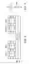
FIG. 6 illustrates a schematic structure drawing of the multiple boosting stages according to an exemplary embodiment of the disclosure. Referring to FIG. 6, a deep doped region 620 is disposed on a p-type substrate 610. The deep doped region 620 may be manufactured as a deep N-well or an N+ buried layer according to different semiconductor processes. The deep doped region 620 is biased at a maximum voltage of the system that that four-phase charge pump circuit 100 is located or the positive boosted voltage VPP in this embodiment. On the deep doped region 620, the boosting stages 120_1 to 120_N are processed in corresponding P-wells. N-wells are respectively disposed between the P-wells for spacing the boosting stages 120_1 to 120_N. In the present embodiment, the main pass transistors NO and N7, the pre-charge transistors N3 and N10, the substrate transistors N1, N2, N8 and N9 and the initial transistors N6 and N13 of the boosting stages 120_1 to 120_N are disposed on the identical deep doped region 620. That is to say, NMOS type charge pumps simply use a single deep N-well, and the occupied chip area of the NMOS type charge pumps is smaller than that of the PMOS type charge pumps.
In the present embodiment, the main pass transistors NO and N7, the pre-charge transistors N3 and N10 and the substrate transistors N1, N2, N8 and N9 of the output stage 110 may also be disposed on the identical deep doped region 620, and the disclosure is not limited thereto.
FIG. 7 illustrates a schematic circuit diagram of each transistor of the boosting stages. Referring to FIG. 6 and FIG. 7, since the main pass transistors NO and N7, the pre-charge transistors N3 and N10, the substrate transistors N1, N2, N8 and N9 and the initial transistors N6 and N13 of the boosting stages 120_1 to 120_N are N-channel MOSFETs and disposed on the identical deep doped region 620, each of the main pass transistors NO and N7, the pre-charge transistors N3 and N10, the substrate transistors N1, N2, N8 and N9 and the initial transistors N6 and N13 of the boosting stages 120_1 to 120_N may be expressed with the circuit diagram as illustrated in FIG. 7 to show that the transistors are disposed on the same deep doped region.
FIG. 8 is a schematic diagram of a four-phase charge pump circuit according to another embodiment of the disclosure. Referring to FIG. 1 and FIG. 8, the four-phase charge pump circuit 800 of the present embodiment is similar to the four-phase charge pump circuit 100 of the embodiment of FIG. 1, and a main difference there between is that the four-phase charge pump circuit 800 further includes an output stage 830. The output stage 830 may be coupled to a boosting stage 820_1 (not shown in FIG. 8) and extract a middle boosted voltage from the boosting stage 820_I in the present embodiment, where I is a positive integer, and 2≦I≦N. The output stage 830 enhances the capability of the extracted middle boosted voltage, so as to output another boosted voltage VPP2 via an output pad OUTB. It should be noticed that the number of the boosting stages and the number of the output stages of the present embodiment are not limited by the disclosure.
Besides, the operation of the four-phase charge pump circuit described in this embodiment of the disclosure is sufficiently taught, suggested, and embodied in the exemplary embodiments illustrated in FIG. 1 to FIG. 7, and therefore no further description is provided herein.
In summary, in the exemplary embodiments of the disclosure, the transistors of the multiple boosting stages are N-channel MOSFETs and disposed on the same deep doped region, and thereby the occupied chip area may be reduced and smaller than that of the charge pump circuit whose deep doped region are separated for each boosting stage. In the exemplary embodiments of the disclosure, the substrate transistors are switched to keep potential at the bodies of the main pass transistors at the low level to mitigate the body effect. The pre-charge transistors may pre-charge gate voltages of the main pass transistors and reduce reverse currents thereof. Moreover, the initial transistors may provide the initial potential to start up waveforms of the boosted voltages.
It will be apparent to those skilled in the art that various modifications and variations can be made to the structure of the disclosure without departing from the scope or spirit of the disclosure. In view of the foregoing, it is intended that the disclosure cover modifications and variations of this disclosure provided they fall within the scope of the following claims and their equivalents.
Claims
What is claimed is:1. A four-phase charge pump circuit comprising:
multiple boosting stages driven by four-phase clock signals, wherein each of the boosting stages comprises two branch charge pumps, and each of the two branch charge pumps comprises:
a main pass transistor having a body, a gate terminal, a source terminal as a first node of the branch charge pump and a drain terminal as a second node of the branch charge pump, wherein the first node and the second node of the branch charge pump connect respectively to a front boosting stage and a rear boosting stage of the boosting stages; and
a pre-charge transistor having a gate terminal, a source terminal and a drain terminal, wherein the source terminal and the drain terminal of the pre-charge transistor are respectively coupled to the gate terminal of the main transistor and the first node of the branch charge pump, and the gate terminal of the pre-charge transistor is coupled to the second node of the branch charge pump,
wherein the main pass transistors and the pre-charge transistors of the boosting stages are disposed on an identical deep doped region.
2. The four-phase charge pump circuit as claimed in claim 1, wherein each of the two branch charge pumps further comprises:
two capacitors coupled respectively to the gate terminal of the main pass transistor and the second node of the branch charge pump.
3. The four-phase charge pump circuit as claimed in claim 2, wherein for each of the boosting stages, the two capacitors of one branch charge pump receive two clock signals of the four-phase clock signals, and the two capacitors of the other branch charge pump receive the other two clock signals of the four-phase clock signals.
4. The four-phase charge pump circuit as claimed in claim 1, wherein each of the two branch charge pumps further comprises:
two substrate transistors, each of the two substrate transistors having a body, a gate terminal, a source terminal and a drain terminal, wherein the source terminals and the bodies of the two substrate transistors are connected together to the body of the main pass transistor, and the drain terminals of the two substrate transistors are connected respectively to the first node and the second node of the branch charge pump,
wherein the gate terminal of one substrate transistor, whose drain terminal connects to the second node, is connected to the first node of one branch charge pump that the one substrate transistor is located, and the gate terminal of the other substrate transistor is connected to the first node of the other branch charge pump.
5. The four-phase charge pump circuit as claimed in claim 4, wherein each of the two branch charge pumps further comprises:
an initial transistor having a body, a gate terminal, a source terminal and a drain terminal, wherein the drain terminal and the source terminal of the initial transistor are respectively coupled to the first node and the second node of the branch charge pump, the gate terminal of the initial transistor is coupled to the drain terminal of the initial transistor, and the body of the initial transistor are connected to the body of the main pass transistor.
6. The four-phase charge pump circuit as claimed in claim 5, wherein potential at the body of each of the main pass transistors and the initial transistors of the boosting stages is kept at a lower substrate level.
7. The four-phase charge pump circuit as claimed in claim 5, wherein the substrate transistors and the initial transistors of the boosting stages are disposed on the identical deep doped region.
8. The four-phase charge pump circuit as claimed in claim 5, wherein the main pass transistors, the pre-charge transistors, the substrate transistors and the initial transistors of the boosting stages are N-channel metal-oxide-semiconductor field-effect transistors (MOSFETs).
9. The four-phase charge pump circuit as claimed in claim 1 further comprising:
an output stage driven by two clock signals of the four-phase clock signals and outputting a boosted voltage, wherein the multiple boosting stages are coupled to the output stage.
10. The four-phase charge pump circuit as claimed in claim 9, wherein the output stage comprises two branch output circuits, and each of the two branch output circuits comprises:
a main pass transistor having a body, a gate terminal, a source terminal as a first node of the branch output circuit and a drain terminal as a second node of the branch output circuit, wherein the first node of the branch output circuit connects to a front boosting stage of the boosting stages, and the second node of the branch output circuit serves as an output end of the output stage to output the boosted voltage; and
a pre-charge transistor having a gate terminal, a source terminal and a drain terminal, wherein the source terminal and the drain terminal of the pre-charge transistor are respectively coupled to the gate terminal of the main transistor and the first node of the branch output circuit, and the gate terminal of the pre-charge transistor is coupled to the second node of the branch output circuit,
wherein the main pass transistors and the pre-charge transistors of the output stage are disposed on the identical deep doped region.
11. The four-phase charge pump circuit as claimed in claim 10, wherein each of the two branch output circuits further comprises:
one capacitor coupled to the gate terminal of the main pass transistor,
wherein the capacitors of the output stage receive two clock signals of the four-phase clock signals.
12. The four-phase charge pump circuit as claimed in claim 10, wherein each of the two branch charge pumps further comprises:
two substrate transistors, each having a body, a gate terminal, a source terminal and a drain terminal, wherein the source terminals and the bodies of the two substrate transistors are connected together to the body of the main pass transistor, and the drain terminals of the two substrate transistors are connected respectively to the first node and the second node of the branch output circuit,
wherein the gate terminal of one substrate transistor, whose drain terminal connects to the second node, is connected to the first node of one branch output circuit that the one substrate transistor is located, and the gate terminal of the other substrate transistor is connected to the first node of the other branch output circuit.
13. The four-phase charge pump circuit as claimed in claim 12, wherein potential at the body of each of the main pass transistors of the output stage is kept at a lower substrate level.
14. The four-phase charge pump circuit as claimed in claim 12, wherein the substrate transistors of the output stage are disposed on the identical deep doped region.
15. The four-phase charge pump circuit as claimed in claim 12, wherein the main pass transistors, the pre-charge transistors and the substrate transistors of the output stage are N-channel MOSFETs.
16. The four-phase charge pump circuit as claimed in claim 1, wherein the four-phase charge pump circuit is a positive charge pump circuit.
Images & Drawings included:

Sources:
- United States Patent and Trademark Office - verify current appl. status at the USPTO↗
Similar patent applications:
- » 20060061410
Four-phase charge pump circuit with reduced body effect - » 20190165672
Four-phase charge pump circuit
Recent applications in this class:
- » 20250175077 2025-05-29
PUMP CAPACITOR CONFIGURATION FOR SWITCHED CAPACITOR CIRCUITS - » 20250175076 2025-05-29
CHARGE PUMP WITH HIGH VOLTAGE CONVERSION RATIO - » 20250167678 2025-05-22
DC-DC TRANSFORMER WITH INDUCTOR FOR THE FACILITATION OF ADIABATIC INTER-CAPACITOR CHARGE TRANSPORT - » 20250158520 2025-05-15
CHARGE ADJUSTMENT TECHNIQUES FOR SWITCHED CAPACITOR POWER CONVERTER - » 20250158519 2025-05-15
POWER MANAGEMENT SYSTEM SWITCHED CAPACITOR VOLTAGE REGULATOR WITH INTEGRATED PASSIVE DEVICE - » 20250141354 2025-05-01
CHARGE PUMP SYSTEM WITH LOW RIPPLE OUTPUT VOLTAGE - » 20250141353 2025-05-01
PROTECTION OF SWITCHED CAPACITOR POWER CONVERTER - » 20250141352 2025-05-01
MULTI-FUNCTION HIGH SIDE FIELD-EFFECT TRANSISTOR DRIVER CIRCUIT - » 20250132667 2025-04-24
Multi-Level Power Converter With Additional Fly Capacitor - » 20250132666 2025-04-24
HYBRID POWER CONVERTERS, LATERAL DEVICES, VERTICAL DEVICES, MULTIPLE COPPER CLIPS, REPLICA DEVICES