Prepregs including UV curable resins useful for manufacturing semi-flexible PCBs
US20160007442A1
2016-01-07
14/838,098
2015-08-27
✅ Patent granted
US 9,764,532 B2
2017-09-19
-
-
Jeff Vonch
McDonnell Boehnen Hulbert & Berghoff LLP
2035-08-27
Abstract:
Prepregs having a UV curable resin layer located adjacent to a thermally curable resin layer wherein the UV curable resin layer includes at least one UV cured resin portion and at least one UV uncured resin as well as methods for preparing flexible printed circuit boards using the prepregs.
Assignee:
- ISOLA USA CORP. 35 🇺🇸 Chandler, AZ, United States
Applicant:
Interested in similar patents?
Get notified when new applications in this technology area are published.
Classification:
H05K1/0298 » CPC further
Printed circuits; Details; Conductive pattern lay-out details not covered by sub groups - Multilayer circuits
H05K1/0298 » CPC further
Printed circuits; Details; Conductive pattern lay-out details not covered by sub groups - Multilayer circuits
H05K1/115 » CPC further
Printed circuits; Details; Printed elements for providing electric connections to or between printed circuits Via connections; Lands around holes or via connections
H05K1/115 » CPC further
Printed circuits; Details; Printed elements for providing electric connections to or between printed circuits Via connections; Lands around holes or via connections
H05K2201/09545 » CPC further
Indexing scheme relating to printed circuits covered by; Shape and layout; Shape and layout details of conductors; Conductive through-holes or vias Plated through-holes or blind vias without lands
H05K2201/09545 » CPC further
Indexing scheme relating to printed circuits covered by; Shape and layout; Shape and layout details of conductors; Conductive through-holes or vias Plated through-holes or blind vias without lands
B32B37/10 » CPC further
Methods or apparatus for laminating, e.g. by curing or by ultrasonic bonding characterised by the pressing technique, e.g. using action of vacuum or fluid pressure
B32B27/08 » CPC further
Layered products comprising synthetic resin as the main or only constituent of a layer, next to another layer of a of synthetic resin
H05K1/02 IPC
Printed circuits Details
H05K1/02 IPC
Printed circuits Details
B32B2305/72 » CPC further
Condition, form or state of the layers or laminate Cured, e.g. vulcanised, cross-linked
B32B2457/08 » CPC further
Electrical equipment PCBs, i.e. printed circuit boards
H05K1/028 » CPC main
Printed circuits; Details; Bendability or stretchability details Bending or folding regions of flexible printed circuits
H05K1/028 » CPC main
Printed circuits; Details; Bendability or stretchability details Bending or folding regions of flexible printed circuits
B32B15/08 » CPC main
Layered products comprising a layer of metal comprising metal as the main or only constituent of a layer, next to another layer of a of synthetic resin
H05K1/11 IPC
Printed circuits; Details Printed elements for providing electric connections to or between printed circuits
H05K1/11 IPC
Printed circuits; Details Printed elements for providing electric connections to or between printed circuits
B32B37/06 » CPC further
Methods or apparatus for laminating, e.g. by curing or by ultrasonic bonding characterised by the heating method
B32B5/024 » CPC further
Layered products characterised by the non- homogeneity or physical structure, i.e. comprising a fibrous, filamentary, particulate or foam layer; Layered products characterised by having a layer differing constitutionally or physically in different parts characterised by structural features of a layer Woven fabric
B32B15/20 » CPC further
Layered products comprising a layer of metal comprising aluminium or copper
B32B37/00 IPC
Methods or apparatus for making layered products; Treatment of the layers or of the layered products
B32B37/00 IPC
Methods or apparatus for laminating, e.g. by curing or by ultrasonic bonding
B32B37/0076 » CPC further
Methods or apparatus for laminating, e.g. by curing or by ultrasonic bonding characterised in that the layers are not bonded on the totality of their surfaces
B32B38/10 » CPC further
Ancillary operations in connection with laminating processes Removing layers, or parts of layers, mechanically or chemically
H05K3/4691 » CPC further
Apparatus or processes for manufacturing printed circuits; Manufacturing multilayer circuits; Composite multilayer circuits, i.e. comprising insulating layers having different properties Rigid-flexible multilayer circuits comprising rigid and flexible layers, e.g. having in the bending regions only flexible layers
B32B2260/023 » CPC further
Layered product comprising an impregnated, embedded, or bonded layer wherein the layer comprises an impregnation, embedding, or binder material; Composition of the impregnated, bonded or embedded layer; Fibrous or filamentary layer Two or more layers
B32B37/14 IPC
Methods or apparatus for laminating, e.g. by curing or by ultrasonic bonding characterised by the properties of the layers
B32B15/14 » CPC further
Layered products comprising a layer of metal next to a fibrous or filamentary layer
B32B37/26 » CPC further
Methods or apparatus for laminating, e.g. by curing or by ultrasonic bonding characterised by the properties of the layers with at least one layer which influences the bonding during the lamination process, e.g. release layers or pressure equalising layers
B32B37/144 » CPC further
Methods or apparatus for laminating, e.g. by curing or by ultrasonic bonding characterised by the properties of the layers using layers with different mechanical or chemical conditions or properties, e.g. layers with different thermal shrinkage, layers under tension during bonding
H05K3/42 IPC
Apparatus or processes for manufacturing printed circuits; Forming printed elements for providing electric connections to or between printed circuits Plated through-holes or plated via connections
H05K3/42 IPC
Apparatus or processes for manufacturing printed circuits; Forming printed elements for providing electric connections to or between printed circuits Plated through-holes or plated via connections
B32B2260/046 » CPC further
Layered product comprising an impregnated, embedded, or bonded layer wherein the layer comprises an impregnation, embedding, or binder material; Impregnation, embedding, or binder material Synthetic resin
B32B2262/101 » CPC further
Composition or structural features of fibres which form a fibrous or filamentary layer or are present as additives; Inorganic fibres Glass fibres
B32B2305/076 » CPC further
Condition, form or state of the layers or laminate; Parts immersed or impregnated in a matrix Prepregs
B32B2305/74 » CPC further
Condition, form or state of the layers or laminate Partially cured
B32B2305/77 » CPC further
Condition, form or state of the layers or laminate Uncured, e.g. green
B32B2307/41 » CPC further
Properties of the layers or laminate having particular optical properties Opaque
B32B2307/412 » CPC further
Properties of the layers or laminate having particular optical properties Transparent
H05K1/0278 » CPC further
Printed circuits; Details; Bendability or stretchability details Rigid circuit boards or rigid supports of circuit boards locally made bendable, e.g. by removal or replacement of material
H05K1/0278 » CPC further
Printed circuits; Details; Bendability or stretchability details Rigid circuit boards or rigid supports of circuit boards locally made bendable, e.g. by removal or replacement of material
H05K1/118 » CPC further
Printed circuits; Details; Printed elements for providing electric connections to or between printed circuits specially for flexible printed circuits, e.g. using folded portions
H05K1/118 » CPC further
Printed circuits; Details; Printed elements for providing electric connections to or between printed circuits specially for flexible printed circuits, e.g. using folded portions
H05K1/147 » CPC further
Printed circuits; Details; Structural association of two or more printed circuits at least one of the printed circuits being bent or folded, e.g. by using a flexible printed circuit
H05K1/147 » CPC further
Printed circuits; Details; Structural association of two or more printed circuits at least one of the printed circuits being bent or folded, e.g. by using a flexible printed circuit
H05K3/429 » CPC further
Apparatus or processes for manufacturing printed circuits; Forming printed elements for providing electric connections to or between printed circuits; Plated through-holes or plated via connections Plated through-holes specially for multilayer circuits, e.g. having connections to inner circuit layers
H05K2201/095 » CPC further
Indexing scheme relating to printed circuits covered by; Shape and layout; Shape and layout details of conductors Conductive through-holes or vias
H05K2201/095 » CPC further
Indexing scheme relating to printed circuits covered by; Shape and layout; Shape and layout details of conductors Conductive through-holes or vias
H05K2201/09063 » CPC further
Indexing scheme relating to printed circuits covered by; Shape and layout; Substrate related Holes or slots in insulating substrate not used for electrical connections
H05K2201/09063 » CPC further
Indexing scheme relating to printed circuits covered by; Shape and layout; Substrate related Holes or slots in insulating substrate not used for electrical connections
H05K2201/09081 » CPC further
Indexing scheme relating to printed circuits covered by; Shape and layout; Substrate related Tongue or tail integrated in planar structure, e.g. obtained by cutting from the planar structure
H05K2201/09081 » CPC further
Indexing scheme relating to printed circuits covered by; Shape and layout; Substrate related Tongue or tail integrated in planar structure, e.g. obtained by cutting from the planar structure
Y10T428/2486 » CPC further
Stock material or miscellaneous articles; Structurally defined web or sheet [e.g., overall dimension, etc.]; Discontinuous or differential coating, impregnation or bond [e.g., artwork, printing, retouched photograph, etc.]; Intermediate layer is discontinuous or differential with outer strippable or release layer
Y10T428/24314 » CPC further
Stock material or miscellaneous articles; Structurally defined web or sheet [e.g., overall dimension, etc.] including aperture; Noncircular aperture [e.g., slit, diamond, rectangular, etc.] Slit or elongated
Y10T428/24322 » CPC further
Stock material or miscellaneous articles; Structurally defined web or sheet [e.g., overall dimension, etc.] including aperture Composite web or sheet
Y10T428/24331 » CPC further
Stock material or miscellaneous articles; Structurally defined web or sheet [e.g., overall dimension, etc.] including aperture; Composite web or sheet including nonapertured component
Y10T428/24612 » CPC further
Stock material or miscellaneous articles; Structurally defined web or sheet [e.g., overall dimension, etc.] including variation in thickness Composite web or sheet
Y10T428/24802 » CPC further
Stock material or miscellaneous articles; Structurally defined web or sheet [e.g., overall dimension, etc.] Discontinuous or differential coating, impregnation or bond [e.g., artwork, printing, retouched photograph, etc.]
B32B27/04 IPC
Layered products comprising synthetic resin as impregnant, bonding, or embedding substance
H05K3/46 IPC
Apparatus or processes for manufacturing printed circuits Manufacturing multilayer circuits
H05K3/46 IPC
Apparatus or processes for manufacturing printed circuits Manufacturing multilayer circuits
B32B5/02 IPC
Layered products characterised by the non- homogeneity or physical structure, i.e. comprising a fibrous, filamentary, particulate or foam layer; Layered products characterised by having a layer differing constitutionally or physically in different parts characterised by structural features of a layer
B32B37/02 » CPC further
Methods or apparatus for laminating, e.g. by curing or by ultrasonic bonding characterised by a sequence of laminating steps, e.g. by adding new layers at consecutive laminating stations
H05K1/14 IPC
Printed circuits; Details Structural association of two or more printed circuits
H05K1/14 IPC
Printed circuits; Details Structural association of two or more printed circuits
B32B37/30 » CPC further
Methods or apparatus for laminating, e.g. by curing or by ultrasonic bonding Partial laminating
B32B2310/0831 » CPC further
Treatment by energy or chemical effects by wave energy or particle radiation using electromagnetic radiation using UV radiation
B32B5/26 » CPC further
Layered products characterised by the non- homogeneity or physical structure, i.e. comprising a fibrous, filamentary, particulate or foam layer; Layered products characterised by having a layer differing constitutionally or physically in different parts characterised by the presence of two or more layers which are next to each other and are fibrous, filamentary, formed of particles or foamed one layer being a fibrous or filamentary layer another layer also being fibrous or filamentary
H05K2201/0195 » CPC further
Indexing scheme relating to printed circuits covered by; Dielectrics; Dielectric layers Dielectric or adhesive layers comprising a plurality of layers, e.g. in a multilayer structure
H05K2201/0195 » CPC further
Indexing scheme relating to printed circuits covered by; Dielectrics; Dielectric layers Dielectric or adhesive layers comprising a plurality of layers, e.g. in a multilayer structure
Y10T428/24851 » CPC further
Stock material or miscellaneous articles; Structurally defined web or sheet [e.g., overall dimension, etc.]; Discontinuous or differential coating, impregnation or bond [e.g., artwork, printing, retouched photograph, etc.] Intermediate layer is discontinuous or differential
Description
This is a continuation of PCT/US2015/38453 filed on Jun. 30, 2015, which claims priority to U.S. provisional application No. 62/019,598, filed on Jul. 1, 2014, the specifications of each of which are incorporated herein by reference.
BACKGROUND OF THE INVENTION
(1) Field of the Invention
This invention concerns films and prepregs including UV curable resins that are useful in the manufacture of flexible PCBs as well as to methods for using the films and prepregs in the manufacture of printed circuit boards.
(2) Description of the Art
Currently, standard flex-rigid multilayer manufacturing processes use flexible polyimide sheets to overlay the copper structures and noflow prepregs. Such standard flex-rigid laminates use expensive materials. Moreover, the manufacturing method is very complex and requires multiple manual processing steps.
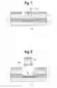
A prior art method for constructing build-ups for an inner-layer flexible multilayer is shown in FIG. 1. The build-ups are formed stepwise by:
-
- structuring a polyamide foil layer including a polyamide planar core (10) a copper layers (11) on each planar polyamide sheet surface and coverlayers (18) overlying the copper layers (11);
- milling a c-staged prepreg layer (12) to form a space (13);
- applying a cover layer (14);
- laminating the partial layup;
- depth milling at the core top and bottoms (shown by black triangles (16));
- stacking-up and lamination of the multilayer; and
- removing the rigid portion of the cores overlying space (13) by milling.
The prior art laminate includes a plated through hole (PTH) (30). The area of the plated through hole in the vicinity of the structured polyamide foil layer creates reliability problems because it requires plasma cleaning. In addition, issues with inadequate metallization of the PTH are common and undesirable barrel cracks can form due to the high thermal expansion of the polyimide and the cover layer in comparison the PTH thermal expansion. Moreover, during the lamination process, little to no pressure is applied to cover layer (14) and polyimide foil layer (10). As a result, PTFE inlays are placed in the stack by hand to increase the stack laminating pressure.
Instead of using the polyamide foil layer (10), a cheaper FR4 material layer can be used instead such as is shown in FIG. 2. However the disadvantage of using the FR4 material is that the resulting layup can only be bent a few times before it becomes damaged. There is a need, therefore, for improved methods for manufacturing flexible multilayer inner-layer laminates that are used to manufacture printed circuit boards that do not suffer from one or more of the problems mentioned above.
SUMMARY OF THE INVENTION
One or more of the shortcomings with flexible laminates made with polyimide foil layers that are noted above can be overcome by replacing the polyimide foil layer with a prepreg comprising a partially (b-staged) or fully (c-staged) cured thermally curable resin layer and an adjacent UV curable resin layer wherein the UV curable resin layer has at least one UV light cured resin portion and at least on UV light uncured resin portion.
Another aspect of this invention is a laminate comprising a flexible core having a first planar surface and a second planar surface the flexible core including an optional copper foil layer on one or both of the first and second planar surfaces, a UV curable resin layer having at first planar surface associated with one of the planar surfaces of the flexible core wherein the UV curable resin layer has at least one UV light cured resin portion and at least on UV light uncured resin portion and a thermally cured resin layer adhered to a second planar surface of the UV curable resin layer.
Yet another aspect of this invention are methods for manufacturing a flexible inner-layer that include the steps of:
-
- (a) applying a mask to a first prepreg including a UV curable resin layer and a thermally curable resin layer wherein the mask is applied to the UV curable resin layer, the mask including at least one UV light transparent portion and at least one UV light opaque portion;
- (b) directing UV light at the mask for a period of time sufficient to cure the UV curable resin layer underlying the UV light transparent portion of the mask to form a UV light treated first prepreg having at least one cured UV resin portion and at least one uncured UV resin portion;
- (c) contacting a core layer with the UV light treated first prepreg such that the at least one cured UV resin portion and the at least one uncured UV resin portion contact the core layer to form a layup; and
- (d) applying heat and/or pressure to the lay-up to form a laminated layup including a rest material portion of the semi-flexible core layer that overlies the at least one cured UV resin portion where the semi-flexible core layer is not substantially laminated to the at least one cured UV resin portion. By “not substantially laminated” we mean the peel strength of any bond between the at least one cured UV resin portion and the semi-flexible core layer is at least 50% and preferably at least 90% less than the peel strength of any bond between the at least one uncured UV resin portion and the semi-flexible core layer for the same laminated layup.
DESCRIPTION OF THE FIGURES
FIG. 1 is a flexible layup made by a prior art method;
FIG. 2 represents an alternative to the flexible layup of FIG. 1 in which the polyamide foil layer is replaced with an FR4 material layer;
FIG. 3 is a side view of a prepreg (100) of this invention including a UV curable resin layer (102) located adjacent to a thermally curable resin layer (104) that is partially cured;
FIG. 4 is cross section of the prepreg of FIG. 3 and further includes a mask layer (108) having a UV light transparent portion (120) and a UV light opaque portion (122);
FIG. 5 is a partially UV cured prepreg resulting from the UV curing step represented by FIG. 4. In FIG. 5, the prepreg includes a UV curable resin layer that has at least one UV polymerized (cured) portion (125) that underlies the UV light transparent portion (120) of mask layer (118) and at least one uncured UV resin portion(s) (127) that underlies the opaque portion(s) mask layer (122);
FIG. 6 is side view of a layup undergoing pin lamination where the layup includes the partially UV cured laminate of FIG. 5;
FIG. 7 and FIG. 8 are side views of the layup during and following milling and rest removal steps; and
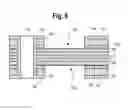
FIG. 9 is a side view of a bendable printed circuit board layup of this invention.
DESCRIPTION OF CURRENT EMBODIMENTS
The present invention relates to the use of special prepregs to replace the flexible polyimide sheets currently used in some flexible printed circuit board manufacturing processes. Laminates and printed circuit boards made with the prepregs of this invention suffer from fewer reliability problems such as barrel cracks in PTH's. In addition, no special plasma cleaning/desmearing steps are necessary.
Referring now to the Figures, there is shown in FIG. 3 a prepreg (100) including a UV curable resin layer (102) located adjacent to a thermally curable resin layer (104) that is at least partially cured (b-staged) and that may, in some applications, be fully cured or c-staged. UV curable resin layer (102) may be of any useful thickness, i.e., thick enough to cause a sufficient amount of melted resin to adhere adjacent layers of a layup. The UV curable resin layer will typically have a thickness ranging from about 2 μm to about 50 μm and more preferably from about 5 μm to about 20 μm. Moreover, the UV curable resin can be applied to an exposed planar surface of thermally curable resin layer (104) by spraying, by applying it with rollers, or by any other known methods.
Any UV curable resin (or photopolymer) that is capable of becoming at least partially liquid and flowable under normal printed circuit board laminating conditions may be used. Examples of useful UV curable resins include, but are not limited to Ultraviolet (UV) and electron beam (EB) energy-cured materials such as urethanes acrylates, polyester acrylates, amino acrylates and epoxy acrylates. In addition, the UV curable materials may include photoinitiators and additives that enhance the performance of the pre and post cured materials.
The properties of a photocured material, such as flexibility, adhesion, and chemical resistance can be provided by functionalized oligomers present in the photocurable composite. As noted above, oligomer photopolymers are typically epoxides, urethanes, polyethers, or polyesters, each of which provides specific properties to the resulting material. Each of these oligomers is typically functionalized by an acrylate. An example shown below is an epoxy oligomer that has been functionalized by acrylic acid. Acrylated epoxies are useful as coatings on metallic substrates, and result in glossy hard coatings.
Acrylated urethane oligomers are typically abrasion resistant, tough, and flexible making ideal coatings for floors, paper, printing plates, and packaging materials. Acrylated polyethers and polyesters result in very hard solvent resistant films, however, polyethers are prone to UV degradation and therefore are rarely used in UV curable material. Often formulations are composed of several types of oligomers to achieve the desirable properties for the material.
As noted above, the prepreg (100) will include a thermally curable resin layer (104). This layer will typically have a thickness of from about 5 μm to about 100 μm and more preferably about 30-60 μm.
The thermally curable resin layers may be made from resins, resin systems or mixtures of resins that are commonly used in the manufacture of printed circuit boards. The resin(s) will typically be a thermoset or thermoplastic resin. Non-limiting examples of useful resins include epoxy resins, cyanurate resins, bismaleimide resins, polyimide resins, phenolic resins, furan resins, xylene formaldehyde resins, ketone formaldehyde resins, urea resins, melamine resins, aniline e resins, alkyd resins, unsaturated polyester resins, diallyl phthalate resins, triallyl cyanurate resins, t iazine resins, polyurethane resins, silicone resins and any combination or mixture thereof.
In one aspect of this invention, the resin is or includes an epoxy resin. Some examples of useful epoxy resins include phenol type epoxy resins such as those based on the diglycidyl ether of bisphenol A, on polyglycidyl ethers of phenol-formaldehyde novolac or cresol-formaldehyde novolac, on the triglycidyl ether of tris(p-hydroxyphenol)methane, or on the tetraglycidyl ether of tetraphenylethane; amine types such as those based on tetraglycidyl-methylenedianiline or on the triglycidyl ether of p-aminoglycol; cycloaliphatic types such as those based on 3,4-epoxycyclohexylmethyl-3,4-epoxycyclohexane carboxylate. The term “epoxy resin” also stands for reaction products of compounds containing an excess of epoxy (for instance, of the aforementioned types) and aromatic dihydroxy compounds. These compounds may be halogen-substituted. One class of useful epoxy-resins are those that are derivatives of bisphenol A, particularly FR-4, FR-4 is made by an advancing reaction of an excess of bisphenol A diglycidyl ether with tetrabromobisphenol A. Mixtures of epoxy resins with bismaleimide resin, cyanate resin and/or bismaleimide triazine resin can also be applied.
The resin compositions, in addition to a base resin will typically include initiators or catalysts, one or more optional flame retardants and solvents. The flame retardant may be any flame retardant material that is known to be useful in resin compositions used to manufacture prepregs and laminates use to manufacture printed circuit boards. The flame retardant(s) may contain halogens or they may be halogen free. Alternatively, or in addition, the resins may include halogens such as bromine in their backbone structure to impart the cured resin with flame retardant properties.
The resin compositions may also include polymerization initiators or catalysts. Examples of some useful initiators or catalysts include, but are not limited to peroxide or azo-type polymerization initiators (catalysts). In general, the initiators/catalysts chosen may be any compound that is known to be useful in resin synthesis or curing whether or not it performs one of these functions.
The resin compositions will include one or more solvents which are typically used to solubilize the appropriate resin composition ingredients and/or to control resin viscosity and/or in order to maintain the resin ingredients in a suspended dispersion. Any solvent known by one of skill in the art to be useful in conjunction with thermosetting resin systems can be used. Particularly useful solvents include methylethylketone (MEK), toluene, dimethylformamide (DMF), or mixtures thereof. As noted below, the resin compositions are used to manufacture prepregs and laminates. During the manufacturing process, the reinforcing materials are impregnated with or otherwise associated with the resin compositions and some or most of the solvent is removed from the resin compositions to form the prepregs and laminates. Thus, when resin composition or laminate weight percent amounts are listed herein, they are reported on a dry-solvent free-basis unless otherwise noted.
The resin compositions may include a variety of other optional ingredients including fillers, tougheners, adhesion promoters, defoaming agents, leveling agents, dyes, and pigments. For example, a fluorescent dye can be added to the resin composition in a trace amount to cause a laminate prepared therefrom to fluoresce when exposed to UV light in a board shop's optical inspection equipment. Other optional ingredients known by persons of skill in the art to be useful in resins that are used to manufacture printed circuit board laminates may also be included in the resin compositions of this invention.
FIGS. 4 and 5 are side view of prepreg (100) of this invention during and after a UV light curing process. FIG. 4 is a side view of the prepreg of FIG. 3 including a mask layer (118) having a UV light transparent portion (120) and a UV light opaque portion (122). In FIG. 4, UV light (121) having a wavelength that is selected to cure the UV curable resin is directed at prepreg (100). The UV light passes through transparent portion (120) of mask (118) and cures the UV curable resin that underlies transparent portion (120). UV light is not able to pass through opaque portion (122) of mask (118) with the result that UV curable resin that lies below mask opaque portion (22) remains uncured and flowable for subsequent lamination steps. The mask layer may be any material that is opaque to UV light of the wavelength necessary to cure the UV curable resin. The transparent portions of mask (118) can be prepared by cutting out our removing portions of the opaque mask material to form windows through which UV light can pass. Other methods know in the art for creating a mask having UV opaque portions and UV transparent portions may be used to make mask (118).
The partially UV cured prepreg resulting from the UV light exposure step is shown in FIG. 5. The partially UV cured prepreg includes UV curable resin layer (102) that has at least one UV polymerized (cured) portion (125) that underlies the UV light transparent portion (120) of mask layer (118) and at least one uncured UV resin portion(s) (127) that underlies the opaque portion(s) (122) of mask layer (118). The resin of the at least one UV cured portion (125) is essentially fully cured or c-staged and will not flow or be tacky in subsequent lamination steps.
FIG. 6 is a side view of the partially UV cured prepreg of FIG. 5 during pin lamination of the prepreg to a semi-flexible core (150) including a first copper layer (154) and a second copper layer (156). In the pin lamination step, optional pins (152) are used to keep prepreg (100) in registration with at least one semi-flexible core (150). In FIG. 6, core (150) is fully cured. During the pin lamination process, the thermally hardening epoxy and not the UV exposed resin works as an adhesive in the stack (black arrows) and adheres the layers together only in the areas of the at least one uncured UV resin portions (127) to form a laminated layup. The at least one UV cured portion (125) of prepreg (100) is cured or hardened prior to lamination and, as a result, there is no adhesion between prepreg (100) and layer (150) in this region because the thermally curable resin cannot flow in this region during lamination. In this way, the uncured portion of the prepreg can be removed from the laminate without first having to create a space (13) in the central portion of the layup as required in the prior art FIG. 1.
FIGS. 7 and 8 are side views of the laminated layup of FIG. 6 wherein a rest material portion (160) of the core material is removed by milling. In FIG. 7, the rest material portion (160) is formed by milling the perimeter (162) of the rest material portion (160) down to the at least one cured UV resin layer portion (125). The milling creates a perimeter around rest material portion (160) that lies above or substantially above the at least one UV cured resin layer portion (125). Since rest material potion (160) is not adhered to the underlying at least one cured UV resin portion (125), separation of rest material portion (160) from the laminated layup is simplified and can be accomplished without further milling to form a semi-flexible area (180) of the laminate as shown in FIG. 8.
FIG. 9 is a side view of a multilayer layup including two semi-flexible cores (170) flanked on both surfaces by prepregs (100, 100′) wherein the thermally curable resin layer (104) of prepreg (100) abuts the surface of semi-flexible core (170) and wherein the a UV curable resin layer (102) is outwardly facing. The layup further includes a second core layer (162) and third core layer (164) each associated with one of the UV curable resin layer surfaces of prepregs (100, 100′) and separated from the UV curable resin layer (102) by an optional layer of copper (164, 164′). Moreover, each core (162) and (164) include an optional outwardly facing copper surface (166, 168). The multilayer layup further includes two opposing cavities (180, 182) formed as described above by removing rest material from the layup as well as a plated through hole (130). As can be seen from FIG. 9, more than one semi-flexible core layer can be used during the manufacture of printed circuit boards having multiple laminate layers.
Prepregs and Laminates
The thermosetting resins and UV curable resins described above are useful for preparing prepregs shown in side-view in FIG. 3. In order to be useful in manufacturing printed circuit boards the resins can be formulated and partially cured—or b-staged—to form prepreg sheets. As prepregs, the sheets can be laid up with additional material sheets to form a “stack” which can be further cured and or laminated to form a fully cured laminate sheet. The resulting laminate sheet can be a final product or it can be used as a layer in further printed circuit board manufacturing steps. In one useful processing system, prepregs (100) can be manufactured in a batch or in a continuous process. For example, sheets of partially cured thermal resins can be prepared and then a UV curable resin can be located on one surface of the partially cured thermal resin sheet to form prepreg (100). Prepregs (100) are optionally manufactured using a core material such a thermally curable resin impregnated woven glass fabric. However, if a core material is used it either can only be associated with a prepreg layer that is opposite the surface of the prepreg though which the UV light must pass to reach the UV curable resin or it must be sufficiently transparent to UV light to allow the UV light to pass through the core material and reach the underlying UV curable resin layer. The core material—e.g. woven glass fabric—can be supplied in a rolled up sheet of woven glass web (fabric) which is unwound into a series of drive rolls. The web then passes into a coating area where the web is passed through a tank which contains the thermosetting resin system of this invention, solvent and other components where the glass web becomes saturated with the resin. The saturated glass web is then passed through a pair of metering rolls which remove excess resin from the saturated glass web and thereafter, the resin coated web travels the length of a drying tower for a selected period of time until the solvent is evaporated from the web. A second and subsequent coating of resin can be applied to the web by repeating these steps until the preparation of the prepreg is complete whereupon the prepreg is wound onto roll. The woven glass web can be replaced with a woven fabric material, paper, plastic sheets, felt, and/or particulate materials such as glass fiber particles or particulate materials.
In another process for manufacturing prepregs, thermosetting resins are premixed in a mixing vessel under ambient temperature and pressure. The viscosity of the pre-mix can be adjusted by adding or removing solvent from the resin. The thermosetting resin (varnish) mix can be used to manufacture unreinforced prepreg sheets and it can also be applied in a thin layer to a Cu foil substrate (RCC—resin coated Cu) using slot-die or other related coating techniques. Thus, it is possible that prepregs used in this invention can include one partially cured thermally curable resin layer having a copper foil on one surface of the sheet. If necessary some or all of the copper foil sheet can be removed to expose the underlying UV curable resin to a UV light source. Indeed, the copper layer can be used as the mask layer and portions of the copper layer can be removed to form UV light transparent portions of the prepreg.
The term “UV curable resin” is used herein to refer to a type of resin—a resin that becomes cured upon exposure to UV light. The term is not intended to indicate the degree of cure of the resin—cured vs. uncured.
The foregoing description of the specific embodiments will reveal the general nature of the disclosure so others can, by applying current knowledge, readily modify and/or adapt for various applications such specific embodiments without departing from the generic concept, and therefore such adaptations and modifications are intended to be comprehended within the meaning and range of equivalents of the disclosed embodiments. It is to be understood that the phraseology or terminology herein is for the purpose of description and not of limitation.
Claims
What is claimed is:1. A method of preparing a laminate sheet comprising the steps of:
(a) applying a mask to a first prepreg including a UV curable resin layer and a thermally curable resin layer wherein the mask is applied to the UV curable resin layer, the mask including at least one UV light transparent portion and at least one UV light opaque portion;
(b) directing UV light at the mask for a period of time sufficient to cure the UV curable resin layer underlying the UV light transparent portion of the mask to form a UV light treated first prepreg having at least one cured UV resin portion and at least one uncured UV resin portion;
(c) contacting a core layer with the UV light treated first prepreg such that the at least one cured UV resin portion and the at least one uncured UV resin portion contact the core layer to form a layup; and
(d) applying heat and/or pressure to the lay-up to form a laminated layup including a rest material portion of the semi-flexible core layer that overlies the at least one cured UV resin portion where the semi-flexible core layer is not substantially laminated to the at least one cured UV resin portion.
2. The method of claim 1 wherein the laminate rest material portion of the layup is removed to form a semi-flexible laminate portion.
3. The method of claim 1 wherein a second prepreg is laminated to the thermally curable resin layer of the first prepreg.
4. The method of claim 3 wherein the second prepreg is laminated to the thermally curable resin layer of the first prepreg prior to method step (a).
5. The method of claim 3 wherein the second prepreg is laminated to the thermally curable resin layer of the first prepreg following method step (b).
6. The method of claim 1 wherein the core layer includes a core having a first and a second planar surface and layer of copper on at least one of the first and second core planar surfaces.
7. The method of claim 6 wherein the core layer includes a layer of copper on each of the first and second core planar surfaces.
8. The method of claim 1 wherein the laminated layup includes a plated through hole.
9. A prepreg comprising a thermally curable resin layer and an adjacent UV curable resin layer wherein thermally curable resin layer has a thickness of from about 2 μm to about 50 μm and the UV curable resin layer has a thickness of from about 5 μm to about 100 μm.
10. The prepreg of claim 9 wherein the UV curable resin layer has at least one UV light cured resin portion and at least on UV light uncured resin portion.
11. The prepreg of claim 9 wherein the thermally curable resin layer is b-staged.
12. The prepreg of claim 9 wherein the thermally curable resin layer is c-staged.
13. A laminated layup including the prepreg of claim 10 and a core layer at least partially adhered to the prepreg UV curable resin layer and including a rest material portion of the core layer that overlies the at least one cured UV resin portion where the semi-flexible core layer is not substantially laminated to the at least one cured UV resin portion.
14. The laminated layup of claim 13 wherein the rest material is removed from the laminated layup to form a cavity.
15. A circuit board including at least one layup of claim 14.
16. A layup for use in manufacturing a printed circuit board comprising:
a semi-flexible core having a first planar surface and a second planar surface;
a first prepreg including a UV curable resin layer and a thermally curable resin layer wherein the thermally curable resin layer is adhered to the first planar surface of the semi-flexible core; and
a second prepreg including a UV curable resin layer and a thermally curable resin layer wherein the thermally curable resin layer is adhered to the second planar surface of the semi-flexible core.
17. The layup of claim 16 wherein a layer of copper separates the first prepreg thermally curable resin layer from the core first layer.
18. The layup of claim 17 wherein a layer of copper separates the second prepreg thermally curable resin layer from the core second layer.
Images & Drawings included:
Sources:
- United States Patent and Trademark Office - verify current appl. status at the USPTO↗
Similar patent applications:
Recent applications in this class:
- » 20250294670 2025-09-18
ELECTRONIC DEVICE - » 20250267787 2025-08-21
METHOD FOR MANUFACTURING FLEXIBLE PRINTED CIRCUIT BOARD - » 20250220808 2025-07-03
FLEXIBLE PRINTED CIRCUIT BOARD INCLUDING LAYER WITH ROUGHNESS AND ELECTRONIC DEVICE INCLUDING SAME - » 20250168973 2025-05-22
DISPLAY DEVICE AND METHOD OF MANUFACTURING THE SAME - » 20250159796 2025-05-15
DATA ADAPTER CABLE - » 20250142720 2025-05-01
IMAGING UNIT - » 20250126704 2025-04-17
ELECTRONIC DEVICE - » 20250113435 2025-04-03
ELASTIC INTERPOSER AND CONDUCTIVE DEVICE THEREOF - » 20250106988 2025-03-27
FLEXIBLE CIRCUIT BOARD, COF MODULE, AND ELECTRONIC DEVICE COMPRISING SAME - » 20250106987 2025-03-27
FLEXIBLE PRINTED CIRCUIT BOARD WITH EMBEDDED OPTICAL WAVEGUIDE STRUCTURE
Recent applications for this Assignee:
- » 20230141772 2023-05-11
SMA resin formulation - » 20230127186 2023-04-27
Prepregs and Laminates Having a UV Curable Resin Layer - » 20200253058 2020-08-06
Prepregs and laminates having a UV curable resin layer - » 20200181342 2020-06-11
High Tg epoxy formulation with good thermal properties - » 20190270873 2019-09-05
SMA resin formulation - » 20190208628 2019-07-04
Prepregs and laminates having homogeneous dielectric properties - » 20180251618 2018-09-06
High Tg epoxy formulation with good thermal properties - » 20180200992 2018-07-19
Prepregs including UV curable resins useful for manufacturing semi-flexible PCBs - » 20170127525 2017-05-04
Prepregs and laminates having a UV curable resin layer - » 20160075839 2016-03-17
High Tg epoxy formulation with good thermal properties