Self-capacitive touch device and calculation method thereof
US20160018927A1
2016-01-21
14/804,421
2015-07-21
✅ Patent granted
US 10,372,273 B2
2019-08-06
-
-
Kwin Xie
JCIPRNET
2036-01-06
Abstract:
A self-capacitive touch device includes a transparent substrate, multiple sensing electrodes and multiple trace lines. The sensing electrodes are alternately disposed on the transparent substrate, and each of the sensing units has a polygonal planar contour having M sides, where M is a positive integer equal to or greater than 4. A side of each of the sensing electrodes corresponds to sides of at least two of the remaining sensing electrodes. The trace lines are electrically connected to the sensing electrodes in a way that a part of segments of the trace lines are disposed in an active region of the self-capacitive touch device.
Assignee:
- ILI TECHNOLOGY CORP. 41 🇹🇼 HSINCHU COUNTY, Taiwan
Applicant:
Interested in similar patents?
Get notified when new applications in this technology area are published.
Classification:
G06F3/0418 » CPC further
Input arrangements for transferring data to be processed into a form capable of being handled by the computer; Output arrangements for transferring data from processing unit to output unit, e.g. interface arrangements; Input arrangements or combined input and output arrangements for interaction between user and computer; Arrangements for converting the position or the displacement of a member into a coded form; Digitisers, e.g. for touch screens or touch pads, characterised by the transducing means; Control or interface arrangements specially adapted for digitisers for error correction or compensation, e.g. based on parallax, calibration or alignment
G06F2203/04101 » CPC further
Indexing scheme relating to -; Indexing scheme relating to - 2.5D-digitiser, i.e. digitiser detecting the X/Y position of the input means, finger or stylus, also when it does not touch, but is proximate to the digitiser's interaction surface and also measures the distance of the input means within a short range in the Z direction, possibly with a separate measurement setup
G06F2203/04111 » CPC further
Indexing scheme relating to -; Indexing scheme relating to - Cross over in capacitive digitiser, i.e. details of structures for connecting electrodes of the sensing pattern where the connections cross each other, e.g. bridge structures comprising an insulating layer, or vias through substrate
G06F2203/04103 » CPC further
Indexing scheme relating to -; Indexing scheme relating to - Manufacturing, i.e. details related to manufacturing processes specially suited for touch sensitive devices
G06F3/0416 » CPC further
Input arrangements for transferring data to be processed into a form capable of being handled by the computer; Output arrangements for transferring data from processing unit to output unit, e.g. interface arrangements; Input arrangements or combined input and output arrangements for interaction between user and computer; Arrangements for converting the position or the displacement of a member into a coded form; Digitisers, e.g. for touch screens or touch pads, characterised by the transducing means Control or interface arrangements specially adapted for digitisers
G06F3/044 » CPC main
Input arrangements for transferring data to be processed into a form capable of being handled by the computer; Output arrangements for transferring data from processing unit to output unit, e.g. interface arrangements; Input arrangements or combined input and output arrangements for interaction between user and computer; Arrangements for converting the position or the displacement of a member into a coded form; Digitisers, e.g. for touch screens or touch pads, characterised by the transducing means by capacitive means
G02F1/13338 » CPC further
Devices or arrangements for the control of the intensity, colour, phase, polarisation or direction of light arriving from an independent light source, e.g. switching, gating or modulating; Non-linear optics for the control of the intensity, phase, polarisation or colour based on liquid crystals, e.g. single liquid crystal display cells; Constructional arrangements; Operation of liquid crystal cells; Circuit arrangements; Constructional arrangements; Manufacturing methods Input devices, e.g. touch panels
G06F3/0412 » CPC further
Input arrangements for transferring data to be processed into a form capable of being handled by the computer; Output arrangements for transferring data from processing unit to output unit, e.g. interface arrangements; Input arrangements or combined input and output arrangements for interaction between user and computer; Arrangements for converting the position or the displacement of a member into a coded form; Digitisers, e.g. for touch screens or touch pads, characterised by the transducing means Digitisers structurally integrated in a display
G09G3/3614 » CPC further
Control arrangements or circuits, of interest only in connection with visual indicators other than cathode-ray tubes for presentation of an assembly of a number of characters, e.g. a page, by composing the assembly by combination of individual elements arranged in a matrix no fixed position being assigned to or needed to be assigned to the individual characters or partial characters by control of light from an independent source using liquid crystals; Control of matrices with row and column drivers Control of polarity reversal in general
G09G3/3648 » CPC further
Control arrangements or circuits, of interest only in connection with visual indicators other than cathode-ray tubes for presentation of an assembly of a number of characters, e.g. a page, by composing the assembly by combination of individual elements arranged in a matrix no fixed position being assigned to or needed to be assigned to the individual characters or partial characters by control of light from an independent source using liquid crystals; Control of matrices with row and column drivers using an active matrix
G06F2203/04105 » CPC further
Indexing scheme relating to -; Indexing scheme relating to - Pressure sensors for measuring the pressure or force exerted on the touch surface without providing the touch position
G09G2300/043 » CPC further
Aspects of the constitution of display devices; Structural and physical details of display devices; Structural details of the set of electrodes Compensation electrodes or other additional electrodes in matrix displays related to distortions or compensation signals, e.g. for modifying TFT threshold voltage in column driver
G09G2300/0408 » CPC further
Aspects of the constitution of display devices; Structural and physical details of display devices; Matrix technologies Integration of the drivers onto the display substrate
G09G2310/0202 » CPC further
Command of the display device; Addressing, scanning or driving the display screen or processing steps related thereto Addressing of scan or signal lines
G09G2310/08 » CPC further
Command of the display device Details of timing specific for flat panels, other than clock recovery
G06F3/045 IPC
Input arrangements for transferring data to be processed into a form capable of being handled by the computer; Output arrangements for transferring data from processing unit to output unit, e.g. interface arrangements; Input arrangements or combined input and output arrangements for interaction between user and computer; Arrangements for converting the position or the displacement of a member into a coded form; Digitisers, e.g. for touch screens or touch pads, characterised by the transducing means using resistive elements, e.g. a single continuous surface or two parallel surfaces put in contact
G06F3/041 IPC
Input arrangements for transferring data to be processed into a form capable of being handled by the computer; Output arrangements for transferring data from processing unit to output unit, e.g. interface arrangements; Input arrangements or combined input and output arrangements for interaction between user and computer; Arrangements for converting the position or the displacement of a member into a coded form Digitisers, e.g. for touch screens or touch pads, characterised by the transducing means
G02F1/1333 IPC
Devices or arrangements for the control of the intensity, colour, phase, polarisation or direction of light arriving from an independent light source, e.g. switching, gating or modulating; Non-linear optics for the control of the intensity, phase, polarisation or colour based on liquid crystals, e.g. single liquid crystal display cells; Constructional arrangements; Operation of liquid crystal cells; Circuit arrangements Constructional arrangements; Manufacturing methods
G09G3/36 IPC
Control arrangements or circuits, of interest only in connection with visual indicators other than cathode-ray tubes for presentation of an assembly of a number of characters, e.g. a page, by composing the assembly by combination of individual elements arranged in a matrix no fixed position being assigned to or needed to be assigned to the individual characters or partial characters by control of light from an independent source using liquid crystals
A61B5/00 IPC
Measuring for diagnostic purposes ; Identification of persons
G06F2203/04107 » CPC further
Indexing scheme relating to -; Indexing scheme relating to - Shielding in digitiser, i.e. guard or shielding arrangements, mostly for capacitive touchscreens, e.g. driven shields, driven grounds
Description
This application claims the benefit of U.S. Provisional Application Ser. No. 62/027,236, filed Jul. 21, 2014, the subject matter of which is incorporated herein by reference.
BACKGROUND OF THE INVENTION
1. Field of the Invention
The invention relates in general to a self-capacitive touch device, and more particularly, to a self-capacitive touch device applied in a wearable device.
2. Description of the Related Art
In the recent years, with extensive developments and applications of consumer electronic products, the number of application products employing touch display devices that integrate touch control and display functions also continues to expand. Some examples of these application products include mobile phones, GPS navigation systems, tablet computers, personal digital assistants (PDAs), and laptop computers. Recently, manufacturers are also dedicated in developing wearable devices having a touch function. Compared to touch devices in common mobile devices, a touch device in a wearable electronic device usually has a smaller touch control region (or referred to as an active region) with an arched contour, resulting in different design layouts in sensing electrodes of these two types of touch devices. Therefore, there is a need for a solution that effectively performs a touch function within a small-range active region of a wearable device.
SUMMARY OF THE INVENTION
The invention is directed to a self-capacitive touch device and a calculation method thereof for overcoming the above drawbacks of the prior art.
According to an embodiment of the present invention, a self-capacitive touch device is provided. The self-capacitive touch device includes a transparent substrate, multiple sensing electrodes and multiple trace lines. The sensing units are alternately disposed on the transparent substrate, and each of the sensing units has a polygonal planar contour having M sides, where M is a positive integer equal to or greater than 4. A side of each of the sensing units corresponds to sides of at least two of the remaining sensing units. The trace lines are electrically connected to the sensing units, respectively, in a way that a part of segments of the trace lines are disposed in an active region of the self-capacitive to touch device.
According to another embodiment of the present invention, a calculation method for a self-capacitive touch device is provided for the abovementioned self capacitive touch device. The calculation method includes: detecting a touch point by the self-capacitive device to cover at least of the sensing unit, such that the sensing unit covered by the touch point generates a sensed capacitance; and multiplying the sensed capacitance by a weight to obtain a touch position of the touch point. The value of the weight is associated with the position of the sensing unit covered by the touch point.
The above and other aspects of the invention will become better understood with regard to the following detailed description of the preferred but non-limiting embodiments. The following description is made with reference to the accompanying drawings.
BRIEF DESCRIPTION OF THE DRAWINGS
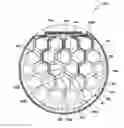
FIG. 1 is a top view of a self-capacitive touch device according to an embodiment of the present invention; and
FIG. 2 is an enlarged partial view of FIG. 1.
DETAILED DESCRIPTION OF THE INVENTION
The following disclosure describes embodiments of a self-capacitive touch device and a calculation method thereof of the present invention for one person skilled in the art to accordingly implement the present invention. These embodiments are given with reference of the accompanying drawings, which also constitute a part of the implementation. Same elements in the drawings are represented by same denotations. It should be noted that, these drawings are for illustration purposes, and are not drawn to actual sizes and ratios.
FIG. 1 shows a top view of a self-capacitive touch device according to an embodiment of the present invention. FIG. 2 shows an enlarged partial view of FIG. 1. As shown in FIG. 1 and FIG. 2, a self-capacitive touch device 100 includes at least a transparent substrate 102, a plurality of sensing units 104, a plurality of border sensing units 105, and a plurality of trace lines 106. The transparent substrate 102, the sensing units 104, the border sensing units 105 and the trace lines 106 are disposed in an active region R1 of the self-capacitive touch device 100 and/or a border region R2 surrounding the active region R1. A planar contour of the active region R1 may include at least an arched side such that the active region R1 has a circular or ellipsoidal planar contour. It should be noted that, throughout the disclosure, the term “active region” refers to a region operable for touch control by a user, and the term “border region” refers to a region primarily for disposing peripheral circuits and/or trace lines.
Preferably, the sensing units 104 are equidistantly discretely disposed on the transparent substrate 102 and are in a design layout of an alternate arrangement or a most densely stacked arrangement, such that the plurality of sensing units 104 having substantially the same planar contour are disposed together to achieve maximum space utilization efficiency. Each of the sensing units 104 may be disposed along sides 1041, 1042, 1043, 1044, 1045 and 1046 of the adjacent sensing units 104, and has a side that is substantially parallel to one of the sides of the adjacent sensing unit 104. According to the embodiment, a large part of the sensing units 104 are disposed in the active region R1, and a small part of the sensing units 104 are disposed in the active region R1 and in the border region R2. The border sensing units 105 may also be disposed along the sides of the adjacent sensing units 104 and/or border sensing units 105. A side of each of the border sensing units 105 is substantially parallel and corresponding to one of the sides of the adjacent sensing units 104 and/or border sensing units 105. According to the embodiment, the border sensing units 105 are disposed along a periphery of the active region R1, or further cross an intersection of the active region R1 and the border region R2.
More specifically, the planar contour of the sensing units 104 may be a regular polygon having M sides, and the planar contour of the border sensing units 105 is an equally proportioned regular polygon obtained from dividing the regular polygon by N. Wherein, M is a positive integer equal to or greater than 4 and is preferably 6; N is a positive integer equal to or greater than 2 and is preferably 2. Further, as shown in FIG. 1, the sensing units 104 having a regular polygonal planar contour are primarily disposed in the active region R1, and the border sensing units 105 having an equally proportioned regular polygonal planar contour are disposed along an intersection R3 between the active region R1 and the border region R2.
Further, the sensing units 104 may be respectively correspondingly connected to the trace lines 106 on a one-on-one basis, so as to allow electric signals to be transmitted between an external circuit and the sensing units 104 via the trace lines 106. More specifically, the trace lines 106 are disposed between two adjacent sensing units 104, in a way that a large part of the trace lines 106 are disposed in the active region R1. Further, each of the trace lines 106 may include an internal connecting portion 1061 and an external connecting portion 1062. The internal connecting portions 1061 may directly come into contact with the corresponding sensing units 104, respectively, or preferably come into contact with vertices of the corresponding sensing units 104. The external connecting portions 108 may extend into the border region R2 to electrically connect to contact pads 108 in the border region R2. The contact pads 108 may serve as welding points for connecting to an external circuit or a control chip to transmit electrical signals to the external circuit for appropriate calculations.
More specifically, the transparent substrate 102 may include a rigid substrate such as glass, or a flexible substrate such as polycarbonate (PC), polyethylene terephthalate (PET), polymethylmesacrylate (PMMA), polysulfone (PES) or other cyclic olefin copolymers, for example. The sensing units 104 and the trace lines 106 may be a single-layer transparent conductive layer, and is preferably a transparent conductive material selected from a group consisted of indium tin oxide (ITO), indium zinc oxide (IZO), cadmium tin oxide (CTO), aluminum zinc oxide (AZO), indium tin zinc oxide (ITZO), zinc oxide, cadmium oxide, hafnium oxide (HfO), indium gallium zinc oxide (InGaZnO), indium gallium zinc magnesium oxide (InGaZnMgO), indium gallium magnesium oxide (InGaMgO) and indium gallium aluminum oxide (InGaAlO), for example. When transparency requirement is not needed, the external connecting portions 1062 of the trace lines 106 and the contact pads 108 in the border region R2 may be selected from a metal or alloy such as copper or gold having a low resistance value, or be formed by the above transparent conductive materials. A part of the external connecting portions 1062 may also be formed by a transparent conductive material, while the remaining part may be formed by a metal or alloy.
According to the above embodiment, the sensing units 104 having a regular polygonal planar contour are primarily disposed in the active region R1, and the border sensing units 105 having an equally proportioned regular polygonal planar contour are disposed along the intersection R3 between the active region R1 and the border region R2. Therefore, for the active region R1 having at least one arched side, the number of sensing units 104 disposed in the active region R1 having an arched planar contour can be maximized to achieve an optimal touch sensing capability.
In addition to the above self-capacitive touch device, a calculation method for a self-capacitive touch device is further provided according to another embodiment of the present invention. Details of the calculation method for a self-capacitive touch device are given below.
As shown in FIG. 2, when a user performs a touch operation on the self-capacitive touch device 100 using a finger or a stylus to apply at least one touch point 200 in an enlarged region R4, the touch point 200 may cover at least one sensing unit 104 such that the sensing units 104 covered by the touch point 200 generate a corresponding sensed capacitances. For example, for the self-capacitive touch device 100 of the embodiment, the touch point 200 may simultaneously cover parts of four sensing units 104. As the sensing units 104 are discretely disposed and the corresponding trace lines 106 are electrically connected to an external circuit, the sensing units 104 covered by the touch point 200 may independently output individual sensed capacitance values. The capacitance values are changed due to a size covered by the touch point 200, and a coordinate position of the touch point 200 may be subsequently determined through calculation according to the capacitance values outputted by the sensing units 104.
An example of the touch point 200 falling in an interval formed by the sensing unit 104 at the (P−1)th column and the (Q+1)th row to the sensing unit 104 at the (P+3)th column and the (Q−1)th row is given as follows. Wherein, P and Q are positive integers equal to or greater than 1. Further, one side 1045 of the sensing unit 104 at the (P+2)th column and the Qth row, one side 1044 of the sensing unit 104 at the (P+1)th column and the (Q−1)th row, and one side 1046 of the sensing unit 104 at the (P+1)th column and the (Q−1)th row are substantially parallel and corresponding to different sides 1042, 1041 and 1043 of the sensing unit 104 at the Pth column and the Qth row, respectively.
For example, as shown in FIG. 2, when the touch point 200 simultaneously covers the sensing unit 104 at the Pth column and the Qth row and the sensing units 104 at the (P+2)th column and the Qth row, equation (1) below may be applied to calculate and determine an X coordinate of the touch point 200:
X = C 1 × X 0 + C 2 × X 1 ∑ i = 1 2 C i equation ( 1 )
In the above equation, X represents the X coordinate that the self-capacitive touch device 100 determines according to the touch point 200, C1 represents the sensed capacitance outputted by the sensing unit 104 at the Pth column and the Qth row, C2 represents the sensed capacitance outputted by the sensing unit 104 at the (P+2)th column and the Qth row, X0 represents an X coordinate weight of the sensing units 104 at the Pth column, and X1 represents an X coordinate weight of the sensing units 104 at the (P+2)th column. The values of X0 and X1 may be determined according to the actual positions of the sensing units 104 and gradually increase or decrease from the left to right, and are preferably positive integers.
Similarly, when the touch point 200 simultaneously covers the sensing unit 104 at the (P+1)th column and the (Q+1)th row and the sensing unit 104 at the (P+1)th column and the (Q−1)th row, equation (2) below may be applied to calculate and determine the touch point 200:
Y = C 3 × Y 0 + C 4 × Y 1 ∑ i = 1 2 C i equation ( 2 )
In equation (2), Y represents a Y coordinate that the self-capacitive touch device 100 determines according to the touch point 200, C represents the sensed capacitance outputted by the sensing unit 104 at the (P+1)th column and the (Q+1)th row, C4 represents the sensed capacitance outputted by the sensing unit 104 at the (P+1)th column and the (Q−1)th row, Y0 represents a Y coordinate weight of the sensing units 104 at the (Q+1)th row, and represents a Y coordinate weight of the sensing units 104 at the (Q−1)th row. The values of Y0 and Y1 may be determined according to the actual positions of the sensing units 104 and gradually increase or decrease from the bottom to top, and are preferably positive integers.
To further increase the touch resolution of the self-capacitive touch device 100, the sensed capacitances sensed by four sensing units 104 may be simultaneously calculated to determine the X coordinate or the Y coordinate of the touch point 200. An example of a calculation method is given below.
For example, as shown in FIG. 2, when the touch point 200 simultaneously covers the sensing unit 104 at the Pth column and the Qth row, the sensing unit 104 at the (P+2)th column and the Qth row, the sensing unit at the (P+1)th column and the (Q+1)th row, and the sensing unit 104 at the (P+1)th column and the (Q−1)th row, equation (3) below may be applied to calculate and determine the X coordinate of the touch point 200:
X = C 1 × X 0 + ( C 3 + C 4 ) × X 2 + C 2 × X 1 ∑ i = 1 4 C i equation ( 3 )
In equation (3), X represents the X coordinate that the self-capacitive touch device 100 determines according to the touch point 200, C1 represents the sensed capacitance outputted by the sensing unit 104 at the Pth column and the Qth row, C2 represents the sensed capacitance outputted by the sensing unit 104 at the (P+2)th column and the Qth row, C3 represents the sensed capacitance outputted by the sensing unit 104 at the (P+1)th column and (Q+1)th row, C4 represents the sensed capacitance outputted by the sensing unit 104 at the (P+1)th column and (Q−1)th row, X0 represents an X coordinate weight of the sensing units 104 at the Pth column, X1 represents an X coordinate weight of the sensing units 104 at the (P+2)th column, and X2 represents an X coordinate weight of the sensing units 104 at the (P+1)th column. The values of X0, X1 and X2 may be determined according to the actual positions of the sensing units 104 and gradually increase or decrease from the left to right, and are preferably positive integers.
Similarly, when the touch point 200 simultaneously covers the sensing unit 104 at the Pth column and the Qth row, the sensing unit 104 at the (P+2)th column and the Qth row, the sensing unit 104 at the (P+1)th column and the (Q+1)th row, and the sensing unit 104 at the (P+1)th column and the (Q−1)th row, equation (4) below may be applied to calculate and determine the touch point 200:
Y = C 3 × Y 0 + ( C 1 + C 2 ) × Y 2 + C 4 × Y 1 ∑ i = 1 4 C i equation ( 4 )
In equation (4), Y represents a Y coordinate that the self-capacitive touch device 100 determines according to the touch point 200, C1 represents the sensed capacitance outputted by the sensing unit 104 at the Pth column and the Qth row, C2 represents the sensed capacitance outputted by the sensing unit 104 at the (P+2)th column and the Qth row, C3 represents the sensed capacitance outputted by the sensing unit 104 at the (P+1)th column and the (Q+1)th row, C4 represents the sensed capacitance outputted by the sensing unit 104 at the (P+1)th column and the (Q−1)th row, Y0 represents a Y coordinate weight of the sensing units 104 at the (Q+1)th row, represents a Y coordinate weight of the sensing units 104 at the (Q−1)th row, and Y2 represents a Y coordinate weight of the sensing units 104 at the Qth row. The values of Y0, Y1 and Y2 may be determined according to the actual positions of the sensing units 104 and gradually increase or decrease from the bottom to top, and are preferably positive integers.
The self-capacitive touch device and the calculation method thereof of the present invention are disclosed in the above embodiments. By adopting such planar contour and design layout of the sensing units 104 and the corresponding calculation method, the self-capacitive touch device 100 is allowed to achieve an optimal touch sensing capability.
The above self-capacitive touch device is described as an independent unit. However, the self-capacitive touch device may also be integrated with a display device or other appropriate devices to form a touch display device. Preferably, the touch display device is a wearable touch display device, which may be worn at a head, torso or limbs of a human body or an animal, for example. For example, the above display device may be a liquid crystal display (LCD) panel, an organic light emitting diode (OLED) display panel, an electro-wetting display panel, an e-ink display panel, a plasma display panel, a field emission display (FED) panel or other appropriate display devices.
While the invention has been described by way of example and in terms of the preferred embodiments, it is to be understood that the invention is not limited thereto. On the contrary, it is intended to cover various modifications and similar arrangements and procedures, and the scope of the appended claims therefore should be accorded the broadest interpretation so as to encompass all such modifications and similar arrangements and procedures.
Claims
What is claimed is:1. A self-capacitive touch device, having an active region, comprising:
a transparent substrate;
a plurality of sensing units, alternately disposed on the substrate, each having a polygonal planar contour with M sides, M being a positive integer equal to or greater than 4, sides of each of the sensing units corresponding to sides of at least two of the remaining sensing units; and
a plurality of trace lines, respectively electrically connected to the sensing units, a part of segments of the trace lines being disposed in the active region.
2. The self-capacitive touch device according to claim 1, wherein the active region comprises at least one arched side.
3. The self-capacitive touch device according to claim 1, wherein the active region has a circular or ellipsoidal planar contour.
4. The self-capacitive touch device according to claim 1, wherein the plurality of sensing units are in a most densely stacked arrangement, and each of the sensing units has one side substantially parallel and corresponding to one side of an adjacent sensing unit of the sensing units.
5. The self-capacitive touch device according to claim 1, wherein the sensing units have a regular hexagonal planar contour.
6. The self-capacitive touch device according to claim 1, further comprising:
a border region, surrounding the active region;
a plurality of border sensing units, disposed along an intersection of the active region and the border region;
wherein, each of the border sensing units has an equally proportioned regular polygonal planar contour obtained from dividing the regular polygonal planar contour by N, where N is a positive integer equal to or greater than 2.
7. The self-capacitive touch device according to claim 6, wherein a side of each of the border sensing units is substantially parallel and corresponding to a side of an adjacent sensing unit of the sensing units.
8. The self-capacitive touch device according to claim 1, wherein the sensing units have a same size and are equidistantly discretely disposed.
9. The self-capacitive touch device according to claim 1, wherein the trace lines are disposed between the sensing units.
10. The self-capacitive touch device according to claim 1, further comprising a border region surrounding the active region; wherein each of the trace lines comprises an internal connecting portion and an external connecting portion, the internal connecting portions are disposed in the active region, and the external connecting portions are disposed in the border region and are formed by a conductive material comprising at least one of metal, alloy and indium tin oxide (ITO).
11. The self-capacitive touch device according to claim 10, wherein each of the internal connecting portions is connected to a vertex of each of the sensing units.
12. The self-capacitive touch device according to claim 1, wherein the trace lines and the sensing units are a single-layer transparent conductive layer, and are formed by a transparent conductive layer.
13. A calculation method for a self-capacitive touch device, applied to the self-capacitive touch device according to claim 1, the calculation method comprises:
detecting a touch point by the self-capacitive touch device, the touch point covering at least one of the plurality of sensing units such that the sensing unit covered by the touch pint generates a sensed capacitance; and
multiplying the sensed capacitance by a weight, wherein a value of the weight is associated with a position of the sensing unit covered by the touch point.
14. The calculation method for a touch display device according to claim 13, wherein the touch point simultaneously covers the sensing unit at a Pth column and a Qth row and the sensing unit at a (P+2)th column and a Qth row, where P and Q are positive integers equal to or greater than 1; the calculation method comprising applying an equation:
X = C 1 × X 0 + C 2 × X 1 ∑ i = 1 2 C i ,
where X represents an X coordinate that the self-capacitive touch device determines according to the touch point, C1 represents the sensed capacitance outputted by the sensing unit 104 at the Pth column and the Qth row, C2 represents the sensed capacitance outputted by the sensing unit at the (P+2)th column and the Qth row, X0 represents an X coordinate weight of the sensing units 104 at the Pth column, and X1 represents an X coordinate weight of the sensing units at the (P+2)th column.
15. The calculation method for a touch display device according to claim 14, wherein one side of the sensing unit at the (P+2)th column and the Qth row is substantially parallel and corresponding to one side of the sensing unit at the Pth column and the Qth row.
16. The calculation method for a touch display device according to claim 13, wherein the touch point simultaneously covers the sensing unit at a Pth column and a Qth row, the sensing unit at a (P+2)th column and a Qth row, the sensing unit at a (P+1)th column and a (Q+1)th row, and the sensing unit at a (P+1)th column and a (Q−1)th row, where P and Q are positive integers equal to or greater than 1; the calculation method comprising applying an equation:
X = C 1 × X 0 + ( C 3 + C 4 ) × X 2 + C 2 × X 1 ∑ i = 1 4 C i ,
where X represents an X coordinate that the self-capacitive touch device determines according to the touch point, C1 represents the sensed capacitance outputted by the sensing unit 104 at the Pth column and the Qth row, C2 represents the sensed capacitance outputted by the sensing unit at the (P+2)th column and the Qth row, C3 represents the sensed capacitance outputted by the sensing unit at the (P+1)th column and the (Q+1)th row, C4 represents the sensed capacitance outputted by the sensing unit at the (P+1)th column and the (Q−1)th row, X0 represents an X coordinate weight of the sensing units at the Pth column, X1 represents an X coordinate weight of the sensing units at the (P+2)th column, and represents an X coordinate weight of the sensing units at the (P+1)th column.
17. The calculation method for a touch display device according to claim 16, wherein values of X0, X1 and X2 are gradually increasing or decreasing positive integers.
18. The calculation method for a touch display device according to claim 16, wherein one side of the sensing unit at the (P+2)th column and the Qth row, one side of the sensing unit at the (P+1)th column and the (Q+1)th row, and one side of the sensing unit 104 at the (P+1)th column and the (Q−1)th row are substantially parallel to different sides of the sensing unit at the Pth column and the Qth row, respectively.
19. The calculation method for a touch display device according to claim 15, wherein the touch point simultaneously covers the sensing unit at a (P+1)th column and a (Q+1)th row and the sensing unit 104 at a (P+1)th column and a (Q−1)th row, wherein P and Q are positive integers equal to or greater than 1; the calculation method comprising applying an equation:
Y = C 3 × Y 0 + C 4 × Y 1 ∑ i = 1 2 C i ,
where Y represents a Y coordinate that the self-capacitive touch device determines according to the touch point 200, C3 represents the sensed capacitance outputted by the sensing unit at the (P+1)th column and the (Q+1)th row, C4 represents the sensed capacitance outputted by the sensing unit at the (P+1)th column and the (Q−1)th row, Y0 represents a Y coordinate weight of the sensing units at the (Q+1)th row, and Y1 represents a Y coordinate weight of the sensing units at the (Q−1)th row.
20. The calculation method for a touch display device according to claim 13, wherein the touch point simultaneously covers the sensing unit 104 at a Pth column and a Qth row, the sensing unit at a (P+2)th column and a Qth row, the sensing unit at a (P+1)th column a (Q+1)th row, and the sensing unit at a (P+1)th column and a (Q−1)th row, where P and Q are positive integers equal to or greater than 1; the calculation method further comprising:
Y = C 3 × Y 0 + ( C 1 + C 2 ) × Y 2 + C 4 × Y 1 ∑ i = 1 4 C i ,
where Y represents a Y coordinate that the self-capacitive touch device determines according to the touch point, C1 represents the sensed capacitance outputted by the sensing unit at the Pth column and the Qth row, C2 represents the sensed capacitance outputted by the sensing unit at the (P+2)th column and the Qth row, C3 represents the sensed capacitance outputted by the sensing unit at the (P+1)th column and the (Q+1)th row, C4 represents the sensed capacitance outputted by the sensing unit at the (P+1)th column and the (Q−1)th row, Y0 represents a Y coordinate weight of the sensing units at the (Q+1)th row, Y1 represents a Y coordinate weight of the sensing units at the (Q−1)th row, and Y2 represents a Y coordinate weight of the sensing units at the Qth row.
Images & Drawings included:


Sources:
- United States Patent and Trademark Office - verify current appl. status at the USPTO↗
Recent applications in this class:
- » 20250278154 2025-09-04
TOUCH CONTROLLER WITH INTEGRATED RFID READ CAPABILITIES, INCLUDING RELATED SYSTEMS, APPARATUSES, AND METHODS - » 20250271970 2025-08-28
MICRO-LED TOUCH DISPLAY DEVICE - » 20250251834 2025-08-07
ELECTROSTATIC CAPACITANCE-TYPE SENSOR-EQUIPPED DISPLAY DEVICE AND METHOD OF DRIVING THE SAME - » 20250231646 2025-07-17
TOUCHLESS DEVICE INTERFACES - » 20250216990 2025-07-03
A DRIVING SIGNAL OUTPUT DEVICE, A DRIVING SIGNAL OUTPUT METHOD, AND A DISPLAY DEVICE - » 20250199647 2025-06-19
EXTERNAL USER INTERFACE FOR HEAD WORN COMPUTING - » 20250190078 2025-06-12
Electronic Devices With Finger Sensors - » 20250138681 2025-05-01
ELECTRONIC DEVICE - » 20250130673 2025-04-24
AUTOMOTIVE TOUCH CIRCUIT DEVICE WITH ESD PROTECTION - » 20250130672 2025-04-24
TOUCH SENSING SYSTEM
Recent applications for this Assignee:
- » 20250251828 2025-08-07
TOUCH SENSING READING DEVICE AND SIGNAL PROCESSING METHOD THEREOF - » 20250231635 2025-07-17
DRIVING DEVICE AND METHOD FOR GENERATING DRIVING VOLTAGE - » 20230051460 2023-02-16
Touch panel and touch input system - » 20220276727 2022-09-01
Touch control device and stylus thereof - » 20200064948 2020-02-27
Mutual capacitive touch panel - » 20190339816 2019-11-07
Mutual capacitive touch panel with narrow border having transparent winding segments - » 20190279600 2019-09-12
DRIVING METHOD OF TOUCH DISPLAY DEVICE, TOUCH DISPLAY CONTROL DEVICE AND TOUCH DISPLAY CONTROL METHOD - » 20190220114 2019-07-18
Mutual capacitive touch panel - » 20190196620 2019-06-27
Mutual capacitive touch panel having double-layer electrode structure - » 20190147211 2019-05-16
FINGERPRINT SENSING DEVICE AND DRIVING METHOD OF FINGERPRINT SENSOR THEREOF