Flexible display and method for preparing the same
US20160021732A1
2016-01-21
14/353,843
2013-09-24
✅ Patent granted
US 9,622,343 B2
2017-04-11
WO; PCT/CN2013/084047; 20130924
WO; WO2015/000225; 20150108
Sing P Chan
Brooks Kushman P.C.
2034-09-24
Abstract:
The present invention provides a flexible display and a method for preparing the same. The method comprises the steps of: providing a first substrate; forming a bonding agent layer on a first surface of the first substrate; providing a second substrate; attaching the surface of the first substrate, on which the bonding agent layer is formed, to the second substrate, wherein the adhesive force between the bonding agent layer and the second substrate is lower than 5 N/20 mm-wide bonding agent layer; forming a display device body on a second surface of the first substrate; and peeling off the first substrate, on which the display device body is formed, from the second substrate, and obtaining the flexible display.
Assignee:
- BOE TECHNOLOGY GROUP CO., LTD 269 🇨🇳 , China
Applicant:
Interested in similar patents?
Get notified when new applications in this technology area are published.
Classification:
H05K1/028 » CPC main
Printed circuits; Details; Bendability or stretchability details Bending or folding regions of flexible printed circuits
H05K1/028 » CPC main
Printed circuits; Details; Bendability or stretchability details Bending or folding regions of flexible printed circuits
B32B15/08 » CPC further
Layered products comprising a layer of metal comprising metal as the main or only constituent of a layer, next to another layer of a of synthetic resin
B32B27/06 » CPC further
Layered products comprising synthetic resin as the main or only constituent of a layer, next to another layer of a
B32B27/28 IPC
Layered products comprising synthetic resin comprising synthetic resins not wholly covered by any one of the sub-groups -
B32B27/281 » CPC further
Layered products comprising synthetic resin comprising synthetic resins not wholly covered by any one of the sub-groups - comprising polyimides
B32B27/286 » CPC further
Layered products comprising synthetic resin comprising synthetic resins not wholly covered by any one of the sub-groups - comprising polysulphones; polysulfides
H05K1/18 IPC
Printed circuits Printed circuits structurally associated with non-printed electric components
H05K1/18 IPC
Printed circuits Printed circuits structurally associated with non-printed electric components
B32B27/365 » CPC further
Layered products comprising synthetic resin comprising polyesters comprising polycarbonates
H05K1/02 IPC
Printed circuits Details
H05K1/02 IPC
Printed circuits Details
H05K1/181 » CPC further
Printed circuits; Printed circuits structurally associated with non-printed electric components associated with surface mounted components
H05K1/181 » CPC further
Printed circuits; Printed circuits structurally associated with non-printed electric components associated with surface mounted components
B32B7/12 » CPC further
Layered products characterised by the relation between layers; Layered products characterised by the relative orientation of features between layers, or by the relative values of a measurable parameter between layers, i.e. products comprising layers having different physical, chemical or physicochemical properties; Layered products characterised by the interconnection of layers; Interconnection of layers using interposed adhesives or interposed materials with bonding properties
B32B2307/7244 » CPC further
Properties of the layers or laminate; Other properties; Permeability to gases, adsorption; Non-permeable Oxygen barrier
B32B2307/7246 » CPC further
Properties of the layers or laminate; Other properties; Permeability to gases, adsorption; Non-permeable Water vapor barrier
B32B2307/7265 » CPC further
Properties of the layers or laminate; Other properties; Permeability to liquids, absorption Non-permeable
B32B2457/20 » CPC further
Electrical equipment Displays, e.g. liquid crystal displays, plasma displays
H05K2201/051 » CPC further
Indexing scheme relating to printed circuits covered by; Flexible printed circuits [FPCs] Rolled
H05K2201/051 » CPC further
Indexing scheme relating to printed circuits covered by; Flexible printed circuits [FPCs] Rolled
B32B38/10 » CPC further
Ancillary operations in connection with laminating processes Removing layers, or parts of layers, mechanically or chemically
H05K3/30 » CPC further
Apparatus or processes for manufacturing printed circuits Assembling printed circuits with electric components, e.g. with resistor
H05K3/30 » CPC further
Apparatus or processes for manufacturing printed circuits Assembling printed circuits with electric components, e.g. with resistor
H05K3/20 » CPC further
Apparatus or processes for manufacturing printed circuits in which conductive material is applied to the insulating support in such a manner as to form the desired conductive pattern by affixing prefabricated conductor pattern
H05K3/20 » CPC further
Apparatus or processes for manufacturing printed circuits in which conductive material is applied to the insulating support in such a manner as to form the desired conductive pattern by affixing prefabricated conductor pattern
B32B2315/08 » CPC further
Other materials containing non-metallic inorganic compounds not provided for in groups - Glass
B32B37/26 IPC
Methods or apparatus for laminating, e.g. by curing or by ultrasonic bonding characterised by the properties of the layers with at least one layer which influences the bonding during the lamination process, e.g. release layers or pressure equalising layers
B32B9/04 IPC
Layered products comprising a layer of a particular substance not covered by groups - comprising such substance as the main or only constituent of a layer, next to another layer of a
B32B9/045 » CPC further
Layered products comprising a layer of a particular substance not covered by groups - comprising such substance as the main or only constituent of a layer, next to another layer of a of synthetic resin
H01L51/00 IPC
Solid state devices using organic materials as the active part, or using a combination of organic materials with other materials as the active part; Processes or apparatus specially adapted for the manufacture or treatment of such devices, or of parts thereof
B32B7/06 » CPC further
Layered products characterised by the relation between layers; Layered products characterised by the relative orientation of features between layers, or by the relative values of a measurable parameter between layers, i.e. products comprising layers having different physical, chemical or physicochemical properties; Layered products characterised by the interconnection of layers; Interconnection of layers permitting easy separation
B32B37/1284 » CPC further
Methods or apparatus for laminating, e.g. by curing or by ultrasonic bonding characterised by using adhesives Application of adhesive
G02F1/1333 » CPC further
Devices or arrangements for the control of the intensity, colour, phase, polarisation or direction of light arriving from an independent light source, e.g. switching, gating or modulating; Non-linear optics for the control of the intensity, phase, polarisation or colour based on liquid crystals, e.g. single liquid crystal display cells; Constructional arrangements; Operation of liquid crystal cells; Circuit arrangements Constructional arrangements; Manufacturing methods
G02F2202/28 » CPC further
Materials and properties Adhesive materials or arrangements
H01L51/003 » CPC further
Solid state devices using organic materials as the active part, or using a combination of organic materials with other materials as the active part; Processes or apparatus specially adapted for the manufacture or treatment of such devices, or of parts thereof; Processes specially adapted for the manufacture or treatment of devices or of parts thereof using a temporary substrate
H01L51/0097 » CPC further
Solid state devices using organic materials as the active part, or using a combination of organic materials with other materials as the active part; Processes or apparatus specially adapted for the manufacture or treatment of such devices, or of parts thereof; Substrates flexible substrates
B29C65/52 IPC
Joining of preformed parts ; Apparatus therefor using adhesives, i.e. using supplementary joining material; solvent bonding applying the adhesive
B32B38/04 » CPC further
Ancillary operations in connection with laminating processes Punching, slitting or perforating
B32B27/36 » CPC further
Layered products comprising synthetic resin comprising polyesters
B32B27/20 » CPC further
Layered products comprising synthetic resin characterised by the use of special additives using fillers, pigments, thixotroping agents
G02F1/133305 » CPC further
Devices or arrangements for the control of the intensity, colour, phase, polarisation or direction of light arriving from an independent light source, e.g. switching, gating or modulating; Non-linear optics for the control of the intensity, phase, polarisation or colour based on liquid crystals, e.g. single liquid crystal display cells; Constructional arrangements; Operation of liquid crystal cells; Circuit arrangements; Constructional arrangements; Manufacturing methods Flexible substrates, e.g. plastics, organic film
H05K2201/10128 » CPC further
Indexing scheme relating to printed circuits covered by; Details of components or other objects attached to or integrated in a printed circuit board; Types of components Display
H05K2201/10128 » CPC further
Indexing scheme relating to printed circuits covered by; Details of components or other objects attached to or integrated in a printed circuit board; Types of components Display
B32B37/12 » CPC further
Methods or apparatus for laminating, e.g. by curing or by ultrasonic bonding characterised by using adhesives
Description
FIELD OF THE INVENTION
The present invention relates to the field of displays, and in particular, to a flexible display and a method for preparing the same.
DESCRIPTION OF THE PRIOR ART
Liquid crystal display (LCD) technologies have been developed rapidly in recent decade, and great improvements have been gained in terms of from screen size to display quality. With continuous efforts, the various performances of LCD have reached the level of traditional cathode ray tube (CRT) displays, and it has a tendency to replace the CRT displays.
As the production of LCD increases continuously, the competition among the manufacturers also increases with each passing day. While making continuous efforts to lower the production cost of the products, each manufacturer also tries to improve the product performances and add more functions, so as to increase the added value of the product and raise its market competitive power.
With the development of flexible display technologies, the flexible display products which are more and more approaching to the traditional display modes will soon go into the life of ordinary people. Because of the intrinsic flexibility of a flexible display, it will bring about a lot of specific user experiences.
At present, there mainly exist two methods for attaching a plastic substrate onto a glass base substrate. In the first method, a plastic substrate and a glass substrate are firmly bonded together by employing a bonding agent with a viscosity as high as possible, and after a display device is prepared, the bonding agent between the plastic substrate and the glass substrate is irradiated in a scan mode by laser from the back of the glass substrate to age and stiffen the bonding agent so that the plastic substrate can be easily peeled off from the surface of the glass substrate. In the second method, a layer of poly(p-xylene) is deposited on a glass substrate via evaporation so as to form a debonding layer, and then a polyamic acid solution is coated on the glass substrate and cured to form polyimide so that the plastic substrate is easily peeled off from the glass substrate by use of the debonding layer.
Both of the above methods have unavoidable disadvantages. For the first method, since a laser process is employed, the production efficiency will be low and the cost will be high. For the second method, since poly(p-xylene) is employed to form a debonding layer and an evaporation is required to prepare the layer poly(p-xylene) on a glass substrate, which is a process of very high cost, the production cost will be very high.
SUMMARY OF THE INVENTION
In order to solve the problem that during the manufacturing of the existing flexible display, a complex process is required to peel off a plastic substrate from a glass substrate and thus the production cost is very high, the present invention provides a flexible display and a method for preparing the same.
The technical solutions employed by the present invention are as follows.
The present invention provides a method for preparing a flexible display, comprising the steps of:
providing a first substrate;
forming a bonding agent layer on a first surface of the first substrate;
providing a second substrate;
attaching the surface of the first substrate, on which the bonding agent layer is formed, to the second substrate, wherein the adhesive force between the bonding agent layer and the second substrate is lower than 5 N/20 mm-wide bonding agent layer;
forming a display device body on a second surface of the first substrate which is opposite to the first surface of the first substrate; and
peeling off the first substrate, on which the display device body is formed, from the second substrate, and obtaining the flexible display.
The invention further provides a flexible display, comprising: a display device body; a first substrate; a bonding agent layer; and a planarization layer and/or a water/oxygen barrier layer arranged between the first substrate and the display device body, wherein a first surface of the first substrate is connected with the bonding agent layer, and a second surface of the first substrate that is opposite to the first surface is connected with the planarization layer and/or the water/oxygen barrier layer; and the adhesive force between the bonding agent layer and the second substrate for bearing the bonding agent layer is lower than 5 N/20 mm-wide bonding agent layer.
The invention has the following beneficial effects: in the preparation method of the flexible display according to the invention, a bonding agent layer with a low adhesive force is formed on a first substrate, and since the adhesive force of the bonding agent is low, it is very easy to peel off the first substrate, on which the display device body is formed, from the second substrate. In comparison with the existing preparation method of the flexible display device, in the preparation method of the present invention, no laser backside processing is required, no costly debonding layer for lowering the adhesive force between the first substrate and the second substrate needs to be prepared, and no undesirable phenomenon such as substrate wrinkling, etc., occurs during the process, so that the production cost is lowered, and the production efficiency is high, thus the preparation method of the present invention is applicable for large-scale production.
BRIEF DESCRIPTION OF THE DRAWINGS
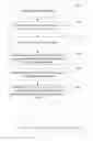
FIG. 1 is a flow chart of a method for preparing a flexible display according to one embodiment of the invention;
FIG. 2 is a schematic diagram showing the preparation method of a bonding agent layer according to one embodiment of the invention;
FIG. 3 is a schematic diagram showing the bonding of a bonding agent layer and a second substrate according to one embodiment of the invention;
FIG. 4 is a schematic diagram showing the preparation method of a display device body according to one embodiment of the invention;
FIG. 5 is a schematic diagram showing the first state in which a display device body is cut according to one embodiment of the invention;
FIG. 6 is a schematic diagram showing the second state in which the display device body is cut according to one embodiment of the invention;
FIG. 7 is a schematic diagram showing the first state in which a flexible display is split according to one embodiment of the invention;
FIG. 8 is a schematic diagram showing the second state in which a flexible display is split according to one embodiment of the invention;
FIG. 9 is a schematic diagram showing the third state in which a flexible display is split according to one embodiment of the invention; and
FIG. 10 is a schematic diagram showing the attachment of a circuit to a flexible display according to one embodiment of the invention.
DETAILED DESCRIPTION OF THE PREFERRED EMBODIMENTS
In order to make the technical problems to be solved, the technical solutions and the advantages of the present invention more apparent, the present invention will be described in detail below in conjunction with the drawings and specific embodiments.
As shown in FIG. 1, it is a flow chart of a method for preparing a flexible display according to one embodiment of the invention, which comprises the steps of:
Step S101: providing a first substrate;
Step S102: forming a bonding agent layer on a first surface of the first substrate;
Step S103: providing a second substrate;
Step S104: attaching the surface of the first substrate on which the bonding agent layer is formed to the second substrate, wherein the adhesive force between the bonding agent layer and the second substrate is lower than 5 N/20 mm-wide bonding agent layer;
Step S105: forming a display device body on a second surface of the first substrate, which is opposite to the first surface of the first substrate; and
Step S106: peeling off the first substrate, on which the display device body is formed, from the second substrate, and obtaining the flexible display.
In the preparation method of the flexible display of the invention, a bonding agent layer with a low adhesive force is formed on a first substrate, and since the adhesive force of the bonding agent is low, it is very easy to peel off the first substrate, on which the display device body is formed, from the second substrate. In comparison with the existing preparation method of the flexible display device, in the invention, no laser backside processing is required, no costly debonding layer for lowering the adhesive force between the first substrate and the second substrate needs to be prepared, and no undesirable phenomenon such as substrate wrinkling, etc., occurs during the process, so that the production cost is lowered, and the production efficiency is high, thus the preparation method of the present invention is applicable for large-scale production.
The bonding agent layer of the invention can lower the adhesive force with the second substrate, for example, a bonding agent may be formed by adding a filler to silica gel, so that the adhesive force between the silica gel and the first substrate is lowered by a material with no or poor adhesive capacity. A flexible display made of silica gel can endure a high temperature of 300-500° C.; and correspondingly the filler in the silica gel also employs a material that can endure high temperature, such as a material that can endure a high temperature of 300-500° C. The bonding agent of the invention may also be formed by adding a filler to acrylic resin so that it may be applied to a touch screen that can endure a temperature of 230° C., and correspondingly the filler thereof may also employ a material that can endure a temperature of 230° C.
The adhesive force between the bonding agent layer of the invention and the second substrate for bearing the bonding agent layer is lower than 5 N/20 mm-wide bonding agent layer, preferably, it is lower than 1 N/20 mm-wide bonding agent layer, and more preferably, it is 0.03 N-0.1 N/20 mm-wide bonding agent layer. (In the field of the present invention, the comparison between adhesive forces is based on the adhesive force generated by a 20 mm-wide object, and since the adhesive force is generated by a bonding agent layer, the adhesive force is based on a 20 mm-wide bonding agent layer. That is, the adhesive force is the force required to pull a 20 mm-wide object off a target object from an end portion in an orientation parallel to the object after adhering the 20 mm-wide object to the target object via a bonding agent.). When the adhesive force of the bonding agent layer of the invention falls within the above range, the desirable attachment between the first substrate and the second substrate may be realized, and the first substrate can be easily peeled off from the second substrate.
The second substrate in the invention is used for bearing the bonding agent layer and the first substrate, and it may be one or more selected from a group consisting of a glass substrate, a metal substrate, a quartz substrate or an organic substrate. In this embodiment, a glass substrate is selected as the second substrate. Preferably, the first substrate of the invention is a plastic substrate with a thermal expansion coefficient between 1-50 ppm/C; and more preferably, it is a plastic substrate with a thermal expansion coefficient between 3-20 ppm/° C. In the invention, a plastic substrate with a thermal expansion coefficient within the above range is employed to keep a thermal expansion coefficient similar to that of a glass substrate, so that a thermal shock may be lowered, and wrinkling of plastic films may be avoided during a vacuum high-temperature process. The material of the plastic substrate may be polyimide (PI), polyethylene naphthalate (PEN), polyethylene terephthalate (PET), fiber-reinforced plastic (FRP), polyethersulfone resin (PES), polyarylester (PAR) or polycarbonate (PC), etc.
As shown in FIG. 2, it is a schematic diagram showing the preparation method of a bonding agent layer according to one embodiment of the invention, wherein a bonding agent is coated via a jet nozzle 3 on the first surface of a first substrate 1 that employs polyimide as the material, thus a bonding agent layer 2 is prepared. The bonding agent may be formed by adding an organic or inorganic filler to silica gel or acrylic resin, for example, by adding a polyterephthalate-type plastic (PET), polyurethane, silicon oxide and titanium oxide, etc., so that the adhesive force of the bonding agent layer formed will be low. Since the adhesive force of the bonding agent layer is low, the first substrate on which the display device body is formed may be very easily peeled off from the second substrate without employing a debonding layer or laser processing, so that the production cost may be lowered, and the operation will be convenient.
As shown in FIG. 3, it is a schematic diagram showing the bonding of a bonding agent layer and a second substrate according to one embodiment of the invention. The surface of the first substrate on which the bonding agent layer is formed is attached to the second substrate 4, and the first substrate 1 is attached via an attachment roller 5 to the second substrate 4 made of glass, so that the bonding agent layer 2 and the second substrate 4 are bonded together. However, the bonding between the bonding agent layer 2 and the second substrate is not limited to the employment of an attachment roller, and other modes may also be employed to attach the bonding agent layer to the second substrate, for example, hand pressing, etc.
As shown in FIG. 4, it is a schematic diagram showing the preparation method of a display device body according to one embodiment of the invention. After the bonding between the bonding agent and the second substrate is accomplished, a planarization layer and/or a water/oxygen barrier layer is formed on a second surface of the first substrate, and then a display device body 7 is formed on the planarization layer and/or the water/oxygen barrier layer. In FIG. 4, label 6 represents a planarization layer and/or a water/oxygen barrier layer, and a water/oxygen barrier layer or a planarization layer, or both, may exist between the bonding agent and the display device body 7, which may be configured according to practical production.
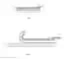
As shown in FIGS. 5 and 6, they are schematic diagrams showing the cutting of a display device according to one embodiment of the invention. In order to peeling off the first substrate, on which a display device body is formed, from the second substrate, the planarization layer and/or the water/oxygen barrier layer on the edge of the first substrate is cut so as to for a slot 8, which may form a certain tilt angle with the surface of the first substrate, for example, 30-60 degrees; and then the first substrate on which the display device body is formed is peeled off from the second substrate along the slot 8 using a mechanical force, thus the flexible display is obtained. Finally, the first substrate 1, together with the display device body 7 on it, is peeled off using a mechanical force, and the preparation of a flexible display is accomplished.
FIG. 7 to FIG. 9 are schematic diagrams showing the splitting a flexible display according to one embodiment of the invention. As shown in FIG. 7 to FIG. 9, after forming a display device body on the planarization layer and/or the water/oxygen barrier layer, the method further includes:
forming a plurality of first fractures 9 that penetrate through the display device body, the planarization layer and/or the water/oxygen barrier layer, the first substrate and the bonding agent layer; and
forming a plurality of second fractures 10 that penetrate through the second substrate, and obtaining a plurality of independent flexible display devices, as shown in FIG. 8, wherein the first fractures 9 have a one-to-one correspondence with the second fractures 10, and each first fracture and each second fracture form a fracture plane;
In this embodiment, the display devices are split via the first fractures and the corresponding second fractures, as shown in FIG. 8. The positions of the first fractures 9 are almost coincident with those of the second fractures 10, so that each display screen can be separated from each other independently. Then, auxiliary components, for example, an integrated circuit chip 11 and a flexible circuit board 12, etc., are attached to each independent display screen, as shown in FIG. 9. Finally, the whole flexible display screen prepared is peeled off from the glass substrate, as shown in FIG. 10. In this embodiment, splitting is accomplished by using two fractures, and two fractures, i.e., an upper fracture and a lower fracture, are formed, which has a low requirement of the cutting wheel; however, when one cut is employed, because the cutting depth is large, a specially designed knife wheel will be needed. In the invention, splitting is realized via two fractures, thus cutting may be realized more easily, and fewer fragments will be generated during cutting.
The invention further provides a flexible display, which includes: a display device body; a first substrate; a bonding agent layer; and a planarization layer and/or a water/oxygen barrier layer arranged between the first substrate and the display device body, wherein a first surface of the first substrate is connected with the bonding agent layer, and a second surface of the first substrate that is opposite to the first surface is connected with the planarization layer and/or the water/oxygen barrier layer, and the adhesive force between the bonding agent layer and the second substrate for bearing the bonding agent layer is lower than 5 N/20 mm-wide bonding agent layer.
Preferably, the adhesive force between the bonding agent layer and the second substrate for bearing the bonding agent layer is lower than 0.1 N/20 mm-wide bonding agent layer.
Preferably, an integrated circuit chip and a flexible circuit board are further set on the display device body.
Preferably, the first substrate is a plastic substrate with an expansion coefficient of 1-50 ppm/° C.
Preferably, the first substrate is a plastic substrate with an expansion coefficient of 3-20 ppm/° C.
Preferably, the material of the first substrate is one or more selected from the group consisting of polyimide, polyethylene naphthalate, polyethylene terephthalate, fiber-reinforced plastic, polyethersulfone resin, polyarylester and polycarbonate.
Preferably, the second substrate is a glass substrate, a metal substrate, a quartz substrate or an organic substrate.
It may be known from the above technical solutions that, in the preparation method of the flexible display of the present invention, a bonding agent layer with a low adhesive force is formed on a first substrate, and since the adhesive force of the bonding agent is low, it is very easy to peel off the first substrate, on which the display device body is formed, from the second substrate. In comparison with the existing preparation method of the flexible display device, in the invention, no laser backside processing is required, no costly debonding layer for lowering the adhesive force between the first substrate and the second substrate needs to be prepared, and no undesirable phenomenon such as substrate wrinkling, etc., occurs during the process, so that the production cost is lowered, and the production efficiency is high, thus the preparation method of the present invention is applicable for large-scale production.
The above description only shows some preferred embodiments of the invention. It should be noted that, for one of ordinary skills in the art, various improvements and modifications may also be made without departing from the principle of the invention, and all these improvements and modifications should be construed as pertaining to the protection scope of the invention.
Claims
1. A method for preparing a flexible display, comprising the steps of:
providing a first substrate;
forming a bonding agent layer on a first surface of the first substrate;
providing a second substrate;
attaching the surface of the first substrate, on which the bonding agent layer is formed, to the second substrate, wherein the adhesive force between the bonding agent layer and the second substrate is lower than 5 N/20 mm-wide bonding agent layer;
forming a display device body on a second surface of the first substrate, which is opposite to the first surface of the first substrate; and
peeling off the first substrate, on which the display device body is formed, from the second substrate and obtaining the flexible display.
2. The method for preparing a flexible display according to claim 1, wherein the bonding agent layer is formed by adding a filler to silica gel.
3. The method for preparing a flexible display according to claim 1, wherein the bonding agent is formed by adding a filler to acrylic resin.
4. The method for preparing a flexible display according to claim 1, wherein the adhesive force between the bonding agent layer and the second substrate is lower than 0.1 N/20 mm-wide bonding agent layer.
5. The method for preparing a flexible display according to claim 1, wherein the step of forming a display device body on a second surface of the first substrate comprises:
forming a planarization layer and/or a water/oxygen barrier layer on the second surface of the first substrate; and
forming a display device body on the planarization layer and/or a water/oxygen barrier layer.
6. The method for preparing a flexible display according to claim 5, wherein the step of peeling off the first substrate, on which the display device body is formed, from the second substrate and obtaining the flexible display comprises:
cutting the planarization layer and/or the water/oxygen barrier layer on the edge of the first substrate to form a slot; and
peeling off the first substrate, on which the display device body is formed, from the second substrate along the slot using a mechanical force and obtaining the flexible display.
7. The method for preparing a flexible display according to claim 5, wherein after forming a display device body on the planarization layer and/or the water/oxygen barrier layer, the following steps are further carried out:
forming a plurality of first fractures that penetrate through the display device body, the planarization layer and/or the water/oxygen barrier layer, the first substrate and the bonding agent layer;
forming a plurality of second fractures that penetrate through the second substrate, and obtaining a plurality of independent flexible display devices, wherein the first fractures have a one-to-one correspondence with the second fractures, and each first fracture and each corresponding second fracture form a fracture plane; and
splitting the display devices via the first fractures and the corresponding second fractures.
8. The method for preparing a flexible display according to claim 6, wherein the step of forming a display device body on the first substrate further comprises: forming an integrated circuit chip and a flexible circuit board on the display device body.
9. The method for preparing a flexible display according to claim 8, wherein after forming an integrated circuit chip and a flexible circuit board on the display device body, the first substrate on which the display device body is formed is peeled off from the second substrate using a mechanical force, thereby obtaining the flexible display.
10. The method for preparing a flexible display according to claim 1, wherein the first substrate is a plastic substrate with an expansion coefficient of 1-50 ppm/° C.
11. The method for preparing a flexible display according to claim 1, wherein the first substrate is a plastic substrate with an expansion coefficient of 3-20 ppm/° C.
12. The method for preparing a flexible display according to claim 1, wherein the material of the first substrate is one or more selected from the group consisting of polyimide, polyethylene naphthalate, polyethylene terephthalate, fiber-reinforced plastic, polyethersulfone resin, polyarylester and polycarbonate.
13. The method for preparing a flexible display according to claim 1, wherein the second substrate is a glass substrate, a metal substrate, a quartz substrate or an organic substrate.
14. A flexible display comprising: a display device body; a first substrate; a bonding agent layer; and a planarization layer and/or a water/oxygen barrier layer arranged between the first substrate and the display device body, wherein a first surface of the first substrate is connected with the bonding agent layer, and a second surface of the first substrate that is opposite to the first surface is connected with the planarization layer and/or the water/oxygen barrier layer; and the adhesive force between the bonding agent layer and the second substrate for bearing the bonding agent layer is lower than 5 N/20 mm-wide bonding agent layer.
15. The flexible display according to claim 14, wherein the adhesive force between the bonding agent layer and the second substrate for bearing the bonding agent layer is lower than 0.1 N/20 mm-wide bonding agent layer.
16. The flexible display according to claim 14, wherein the first substrate is a plastic substrate with an expansion coefficient of 1-50 ppm/° C.
17. The flexible display according to claim 15, wherein the first substrate is a plastic substrate with an expansion coefficient of 3-20 ppm/° C.
18. The flexible display according to claim 14, wherein an integrated circuit chip and a flexible circuit board are further provided on the display device body.
19. The method for preparing a flexible display according to claim 7, wherein the step of forming a display device body on the first substrate further comprises: forming an integrated circuit chip and a flexible circuit board on the display device body.
20. The flexible display according to claim 15, wherein an integrated circuit chip and a flexible circuit board are further provided on the display device body.
Images & Drawings included:


Sources:
- United States Patent and Trademark Office - verify current appl. status at the USPTO↗
Similar patent applications:
- » 20190067240
Flexible display panel and preparation method thereof, flexible display device - » 20220393121
SUPPORTING MEMBER OF FLEXIBLE DISPLAY MODULE AND PREPARATION METHOD THEREFOR, FLEXIBLE DISPLAY MODULE, AND DISPLAY DEVICE - » 20200356142
Flexible display, preparation method thereof and electronic device having the same - » 20250264912
FLEXIBLE DISPLAY ASSEMBLY, FLEXIBLE DISPLAY DEVICE AND METHOD FOR PREPARING FLEXIBLE DISPLAY DEVICE - » 20230124365
FLEXIBLE DISPLAY ASSEMBLY, FLEXIBLE DISPLAY DEVICE AND METHOD FOR PREPARING FLEXIBLE DISPLAY DEVICE - » 20210336202
Flexible display panel, with patterned organic encapsulation layer, flexible display device including same, and method of preparing flexible display panel - » 20190355925
Flexible display module, flexible display device and method for preparing the flexible display module - » 20170269287
Flexible display panel, method of preparing the same and flexible display device - » 20120234480
Method for fixing glass substrates and method for preparing flexible display device - » 20140141683
Method for preparing flexible display device
Recent applications in this class:
- » 20250294670 2025-09-18
ELECTRONIC DEVICE - » 20250267787 2025-08-21
METHOD FOR MANUFACTURING FLEXIBLE PRINTED CIRCUIT BOARD - » 20250220808 2025-07-03
FLEXIBLE PRINTED CIRCUIT BOARD INCLUDING LAYER WITH ROUGHNESS AND ELECTRONIC DEVICE INCLUDING SAME - » 20250168973 2025-05-22
DISPLAY DEVICE AND METHOD OF MANUFACTURING THE SAME - » 20250159796 2025-05-15
DATA ADAPTER CABLE - » 20250142720 2025-05-01
IMAGING UNIT - » 20250126704 2025-04-17
ELECTRONIC DEVICE - » 20250113435 2025-04-03
ELASTIC INTERPOSER AND CONDUCTIVE DEVICE THEREOF - » 20250106988 2025-03-27
FLEXIBLE CIRCUIT BOARD, COF MODULE, AND ELECTRONIC DEVICE COMPRISING SAME - » 20250106987 2025-03-27
FLEXIBLE PRINTED CIRCUIT BOARD WITH EMBEDDED OPTICAL WAVEGUIDE STRUCTURE
Recent applications for this Assignee:
- » 20230341983 2023-10-26
Touch module comprising touch units, manufacturing method thereof and touch display device having the touch module - » 20220396729 2022-12-15
Method for preparing ZnSe quantum dot, ZnSe quantum dot, ZnSe structure and display device - » 20220359789 2022-11-10
Inorganic light-emitting diode substrate and manufacturing method thereof, and inorganic light-emitting diode display device - » 20220336546 2022-10-20
Display panel having five first, four second and four third sub-pixels arranged in a virtual rectangle with five first sub-pixels having different areas from each other and four third sub-pixels having different areas from each other - » 20220269123 2022-08-25
Chip on film and display device - » 20190011118 2019-01-10
Backlight module and display device - » 20180323745 2018-11-08
Household photovoltaic system and smart micro-grid system - » 20180315959 2018-11-01
Substrate lifting device, substrate packaging apparatus and substrate packaging method - » 20180315619 2018-11-01
Thin film transistor, manufacturing method thereof, and method for manufacturing array substrate - » 20180308404 2018-10-25
Scanning direction control circuit, driving method thereof, light-on testing device and display device