Semiconductor TSV device package for circuit board connection
US20160035693A1
2016-02-04
14/878,917
2015-10-08
✅ Patent granted
US 9,508,690 B2
2016-11-29
-
-
Joseph Schoenholtz
Damion Josephs
2035-10-08
Abstract:
An electronic device includes a circuit board and a semiconductor device package. The semiconductor device package includes a laminate layer. The semiconductor device package includes a semiconductor die having an active side, an inactive side opposite the active side, and through-silicon vias (TSVs) conductively connecting the active side to the inactive side and conductively connecting the semiconductor die to one of the laminate layer and the circuit board. The semiconductor device package includes a laminate layer having a side attached to the active side or the inactive side semiconductor die. The semiconductor device package includes solder balls at the side of the laminate layer attached to the semiconductor die, around the semiconductor die, and attached to the circuit board.
Inventors:
- Richard S. Graf 51 🇺🇸 Gray, ME, United States
- David J. West 12 🇺🇸 Essex Junction, VT, United States
Assignee:
- INTERNATIONAL BUSINESS MACHINES CORPORATION 136,239 🇺🇸 ARMONK, NY, United States
Applicant:
Interested in similar patents?
Get notified when new applications in this technology area are published.
Classification:
H01L24/81 » CPC main
Arrangements for connecting or disconnecting semiconductor or solid-state bodies; Methods or apparatus related thereto; Methods for connecting semiconductor or other solid state bodies using means for bonding being attached to, or being formed on, the surface to be connected using a bump connector
H01L23/481 » CPC further
Details of semiconductor or other solid state devices; Arrangements for conducting electric current to or from the solid state body in operation, e.g. leads, terminal arrangements ; Selection of materials therefor Internal lead connections, e.g. via connections, feedthrough structures
H01L24/11 » CPC further
Arrangements for connecting or disconnecting semiconductor or solid-state bodies; Methods or apparatus related thereto; Means for bonding being attached to, or being formed on, the surface to be connected, e.g. chip-to-package, die-attach, "first-level" interconnects; Manufacturing methods related thereto; Bump connectors ; Manufacturing methods related thereto Manufacturing methods
H01L24/03 » CPC further
Arrangements for connecting or disconnecting semiconductor or solid-state bodies; Methods or apparatus related thereto; Means for bonding being attached to, or being formed on, the surface to be connected, e.g. chip-to-package, die-attach, "first-level" interconnects; Manufacturing methods related thereto; Bonding areas ; Manufacturing methods related thereto Manufacturing methods
H01L2224/81191 » CPC further
Indexing scheme for arrangements for connecting or disconnecting semiconductor or solid-state bodies and methods related thereto as covered by; Methods for connecting semiconductor or other solid state bodies using means for bonding being attached to, or being formed on, the surface to be connected using a bump connector; Arrangement of the bump connectors prior to mounting wherein the bump connectors are disposed only on the semiconductor or solid-state body
H01L2224/81192 » CPC further
Indexing scheme for arrangements for connecting or disconnecting semiconductor or solid-state bodies and methods related thereto as covered by; Methods for connecting semiconductor or other solid state bodies using means for bonding being attached to, or being formed on, the surface to be connected using a bump connector; Arrangement of the bump connectors prior to mounting wherein the bump connectors are disposed only on another item or body to be connected to the semiconductor or solid-state body
H01L2225/0652 » CPC further
Details relating to assemblies covered by the group but not provided for in its subgroups; All the devices being of a type provided for in the same subgroup of groups - the devices not having separate containers the devices being of a type provided for in group; Stacked arrangements of devices Bump or bump-like direct electrical connections from substrate to substrate
H01L23/48 IPC
Details of semiconductor or other solid state devices Arrangements for conducting electric current to or from the solid state body in operation, e.g. leads, terminal arrangements ; Selection of materials therefor
H01L25/0657 » CPC main
Assemblies consisting of a plurality of individual semiconductor or other solid state devices ; Multistep manufacturing processes thereof all the devices being of a type provided for in the same subgroup of groups - , e.g. assemblies of rectifier diodes the devices not having separate containers the devices being of a type provided for in group Stacked arrangements of devices
H01L23/49833 » CPC further
Details of semiconductor or other solid state devices; Arrangements for conducting electric current to or from the solid state body in operation, e.g. leads, terminal arrangements ; Selection of materials therefor consisting of soldered constructions; Leads, on insulating substrates, the chip support structure consisting of a plurality of insulating substrates
H01L25/50 » CPC further
Assemblies consisting of a plurality of individual semiconductor or other solid state devices ; Multistep manufacturing processes thereof Multistep manufacturing processes of assemblies consisting of devices, each device being of a type provided for in group or
H01L24/17 » CPC further
Arrangements for connecting or disconnecting semiconductor or solid-state bodies; Methods or apparatus related thereto; Means for bonding being attached to, or being formed on, the surface to be connected, e.g. chip-to-package, die-attach, "first-level" interconnects; Manufacturing methods related thereto; Bump connectors ; Manufacturing methods related thereto; Structure, shape, material or disposition of the bump connectors after the connecting process of a plurality of bump connectors
H01L2225/06517 » CPC further
Details relating to assemblies covered by the group but not provided for in its subgroups; All the devices being of a type provided for in the same subgroup of groups - the devices not having separate containers the devices being of a type provided for in group; Stacked arrangements of devices Bump or bump-like direct electrical connections from device to substrate
H01L2225/06541 » CPC further
Details relating to assemblies covered by the group but not provided for in its subgroups; All the devices being of a type provided for in the same subgroup of groups - the devices not having separate containers the devices being of a type provided for in group; Stacked arrangements of devices Conductive via connections through the device, e.g. vertical interconnects, through silicon via [TSV]
H01L2225/06572 » CPC further
Details relating to assemblies covered by the group but not provided for in its subgroups; All the devices being of a type provided for in the same subgroup of groups - the devices not having separate containers the devices being of a type provided for in group; Stacked arrangements of devices Auxiliary carrier between devices, the carrier having an electrical connection structure
H01L2924/15311 » CPC further
Indexing scheme for arrangements or methods for connecting or disconnecting semiconductor or solid-state bodies as covered by; Details of package parts other than the semiconductor or other solid state devices to be connected; Die mounting substrate; Connection portion the connection portion being formed only on the surface of the substrate opposite to the die mounting surface being a ball array, e.g. BGA
H01L2924/15321 » CPC further
Indexing scheme for arrangements or methods for connecting or disconnecting semiconductor or solid-state bodies as covered by; Details of package parts other than the semiconductor or other solid state devices to be connected; Die mounting substrate; Connection portion the connection portion being formed on the die mounting surface of the substrate being a ball array, e.g. BGA
H01L2924/15331 » CPC further
Indexing scheme for arrangements or methods for connecting or disconnecting semiconductor or solid-state bodies as covered by; Details of package parts other than the semiconductor or other solid state devices to be connected; Die mounting substrate; Connection portion the connection portion being formed on the die mounting surface of the substrate the connection portion being formed both on the die mounting surface of the substrate and outside the die mounting surface of the substrate being a ball array, e.g. BGA
H01L25/065 IPC
Assemblies consisting of a plurality of individual semiconductor or other solid state devices ; Multistep manufacturing processes thereof all the devices being of a type provided for in the same subgroup of groups - , e.g. assemblies of rectifier diodes the devices not having separate containers the devices being of a type provided for in group
H01L23/498 IPC
Details of semiconductor or other solid state devices; Arrangements for conducting electric current to or from the solid state body in operation, e.g. leads, terminal arrangements ; Selection of materials therefor consisting of soldered constructions Leads, on insulating substrates,
H01L25/00 IPC
Assemblies consisting of a plurality of individual semiconductor or other solid state devices ; Multistep manufacturing processes thereof
H01L23/00 IPC
Details of semiconductor or other solid state devices
H01L23/49816 » CPC further
Details of semiconductor or other solid state devices; Arrangements for conducting electric current to or from the solid state body in operation, e.g. leads, terminal arrangements ; Selection of materials therefor consisting of soldered constructions; Leads, on insulating substrates,; Additional leads joined to the metallisation on the insulating substrate, e.g. pins, bumps, wires, flat leads Spherical bumps on the substrate for external connection, e.g. ball grid arrays [BGA]
H01L24/06 » CPC further
Arrangements for connecting or disconnecting semiconductor or solid-state bodies; Methods or apparatus related thereto; Means for bonding being attached to, or being formed on, the surface to be connected, e.g. chip-to-package, die-attach, "first-level" interconnects; Manufacturing methods related thereto; Bonding areas ; Manufacturing methods related thereto; Structure, shape, material or disposition of the bonding areas prior to the connecting process of a plurality of bonding areas
H01L25/105 » CPC further
Assemblies consisting of a plurality of individual semiconductor or other solid state devices ; Multistep manufacturing processes thereof all the devices being of a type provided for in the same subgroup of groups - , e.g. assemblies of rectifier diodes the devices having separate containers the devices being of a type provided for in group
H01L23/3128 » CPC further
Details of semiconductor or other solid state devices; Encapsulations, e.g. encapsulating layers, coatings, e.g. for protection characterised by the arrangement or shape the device being completely enclosed a substrate forming part of the encapsulation the substrate having spherical bumps for external connection
H01L24/05 » CPC further
Arrangements for connecting or disconnecting semiconductor or solid-state bodies; Methods or apparatus related thereto; Means for bonding being attached to, or being formed on, the surface to be connected, e.g. chip-to-package, die-attach, "first-level" interconnects; Manufacturing methods related thereto; Bonding areas ; Manufacturing methods related thereto; Structure, shape, material or disposition of the bonding areas prior to the connecting process of an individual bonding area
H01L24/13 » CPC further
Arrangements for connecting or disconnecting semiconductor or solid-state bodies; Methods or apparatus related thereto; Means for bonding being attached to, or being formed on, the surface to be connected, e.g. chip-to-package, die-attach, "first-level" interconnects; Manufacturing methods related thereto; Bump connectors ; Manufacturing methods related thereto; Structure, shape, material or disposition of the bump connectors prior to the connecting process of an individual bump connector
H01L24/16 » CPC further
Arrangements for connecting or disconnecting semiconductor or solid-state bodies; Methods or apparatus related thereto; Means for bonding being attached to, or being formed on, the surface to be connected, e.g. chip-to-package, die-attach, "first-level" interconnects; Manufacturing methods related thereto; Bump connectors ; Manufacturing methods related thereto; Structure, shape, material or disposition of the bump connectors after the connecting process of an individual bump connector
H01L24/73 » CPC further
Arrangements for connecting or disconnecting semiconductor or solid-state bodies; Methods or apparatus related thereto Means for bonding being of different types provided for in two or more of groups , , , , , , ,
H01L24/92 » CPC further
Arrangements for connecting or disconnecting semiconductor or solid-state bodies; Methods or apparatus related thereto; Methods for connecting semiconductor or solid state bodies including different methods provided for in two or more of groups - Specific sequence of method steps
H01L2224/0401 » CPC further
Indexing scheme for arrangements for connecting or disconnecting semiconductor or solid-state bodies and methods related thereto as covered by; Means for bonding being attached to, or being formed on, the surface to be connected, e.g. chip-to-package, die-attach, "first-level" interconnects; Manufacturing methods related thereto; Bonding areas; Manufacturing methods related thereto; Structure, shape, material or disposition of the bonding areas prior to the connecting process Bonding areas specifically adapted for bump connectors, e.g. under bump metallisation [UBM]
H01L2224/1703 » CPC further
Indexing scheme for arrangements for connecting or disconnecting semiconductor or solid-state bodies and methods related thereto as covered by; Means for bonding being attached to, or being formed on, the surface to be connected, e.g. chip-to-package, die-attach, "first-level" interconnects; Manufacturing methods related thereto; Bump connectors; Manufacturing methods related thereto; Structure, shape, material or disposition of the bump connectors after the connecting process of a plurality of bump connectors; Structure Bump connectors having different sizes, e.g. different diameters, heights or widths
H01L2224/73204 » CPC further
Indexing scheme for arrangements for connecting or disconnecting semiconductor or solid-state bodies and methods related thereto as covered by; Means for bonding being of different types provided for in two or more of groups; Location after the connecting process on the same surface; Bump and layer connectors the bump connector being embedded into the layer connector
H01L2224/92125 » CPC further
Indexing scheme for arrangements for connecting or disconnecting semiconductor or solid-state bodies and methods related thereto as covered by; Methods for connecting semiconductor or solid state bodies including different methods provided for in two or more of groups - ; Specific sequence of method steps; Connecting a surface with connectors of different types; Sequential connecting processes the first connecting process involving a bump connector the second connecting process involving a layer connector
H01L2225/06513 » CPC further
Details relating to assemblies covered by the group but not provided for in its subgroups; All the devices being of a type provided for in the same subgroup of groups - the devices not having separate containers the devices being of a type provided for in group; Stacked arrangements of devices Bump or bump-like direct electrical connections between devices, e.g. flip-chip connection, solder bumps
H01L2225/06548 » CPC further
Details relating to assemblies covered by the group but not provided for in its subgroups; All the devices being of a type provided for in the same subgroup of groups - the devices not having separate containers the devices being of a type provided for in group; Stacked arrangements of devices Conductive via connections through the substrate, container, or encapsulation
H01L2225/107 » CPC further
Details relating to assemblies covered by the group but not provided for in its subgroups; All the devices being of a type provided for in the same subgroup of groups - the devices having separate containers the devices being of a type provided for in group the containers being in a stacked arrangement; Details of electrical connections between containers Indirect electrical connections, e.g. via an interposer, a flexible substrate, using TAB
H01L2225/1023 » CPC further
Details relating to assemblies covered by the group but not provided for in its subgroups; All the devices being of a type provided for in the same subgroup of groups - the devices having separate containers the devices being of a type provided for in group the containers being in a stacked arrangement the lowermost container comprising a device support the support being an insulating substrate
H01L2225/1041 » CPC further
Details relating to assemblies covered by the group but not provided for in its subgroups; All the devices being of a type provided for in the same subgroup of groups - the devices having separate containers the devices being of a type provided for in group the containers being in a stacked arrangement Special adaptations for top connections of the lowermost container, e.g. redistribution layer, integral interposer
H01L2924/1431 » CPC further
Indexing scheme for arrangements or methods for connecting or disconnecting semiconductor or solid-state bodies as covered by; Details of semiconductor or other solid state devices to be connected; Device type; Integrated circuits; Digital devices Logic devices
H01L25/10 IPC
Assemblies consisting of a plurality of individual semiconductor or other solid state devices ; Multistep manufacturing processes thereof all the devices being of a type provided for in the same subgroup of groups - , e.g. assemblies of rectifier diodes the devices having separate containers
H01L23/31 IPC
Details of semiconductor or other solid state devices; Encapsulations, e.g. encapsulating layers, coatings, e.g. for protection characterised by the arrangement or shape
Description
BACKGROUND
Electronic devices can include semiconductor dies mounted to circuit boards. The semiconductor dies are typically packaged. The resulting semiconductor device packages are then mounted to the circuit boards.
SUMMARY
An example semiconductor device package includes a semiconductor die having an active side, an inactive side opposite the active side, and through-silicon vias (TSVs) conductively connecting the active side to the inactive side. The semiconductor device package includes a laminate layer having a side attached to the semiconductor die at the active side thereof via solder bumps. The semiconductor device package includes solder balls at the side of the laminate layer attached to the semiconductor die, around the semiconductor die.
An example electronic device includes a circuit board and a semiconductor device package. The semiconductor device package includes a laminate layer. The semiconductor device package includes a semiconductor die having an active side, an inactive side opposite the active side, and TSVs conductively connecting the active side to the inactive side and conductively connecting the semiconductor die to one of the laminate layer and the circuit board. The semiconductor device package includes a laminate layer having a side attached to the semiconductor die. The semiconductor device package includes solder balls at the side of the laminate layer attached to the semiconductor die, around the semiconductor die, and attached to the circuit board.
An example method includes preparing a semiconductor die having an active side, an inactive side opposite the active side, and TSVs conductively connecting the active side to the inactive side. The method includes attaching a laminate layer to the semiconductor die. The method includes attaching a circuit board to the semiconductor die.
BRIEF DESCRIPTION OF THE SEVERAL VIEWS OF THE DRAWINGS
The drawings referenced herein form a part of the specification. Features shown in the drawing illustrate only some embodiments of the disclosure, and not of all embodiments of the disclosure, unless the detailed description explicitly indicates otherwise, and readers of the specification should not make implications to the contrary.
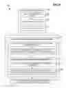
FIG. 1 is a diagram of an example electronic device including a semiconductor device package with a semiconductor die having through-silicon vias (TSVs) attached to a circuit board of the device.
FIG. 2 is a diagram of an example electronic device including a semiconductor device package with a first semiconductor die having TSVs attached to a circuit board of the device, and a second semiconductor die conductively connected to the first laminate in a “double sided chip” manner.
FIG. 3 is a diagram of an example electronic device including a first semiconductor device package with a semiconductor die having TSVs attached to a circuit board of the device, and a second semiconductor device package with another semiconductor die attached to the first package in a “package on package” manner.
FIG. 4 is a diagram of an example electronic device including a semiconductor device package with a semiconductor die having TSVs attached to laminate layer of the package, and a circuit board attached to an active side of the die.
FIG. 5 is a flowchart of an example method for fabricating the electronic device of FIGS. 1, 2, 3, 4, and 5.
DETAILED DESCRIPTION
The following detailed description of exemplary embodiments of the disclosure refers to the accompanying drawings that form a part of the description. The drawings illustrate specific exemplary embodiments in which the disclosure may be practiced. The detailed description, including the drawings, describes these embodiments in sufficient detail to enable those skilled in the art to practice the disclosure. Those skilled in the art may further utilize other embodiments of the disclosure, and make logical, mechanical, and other changes without departing from the spirit or scope of the disclosure.
As noted in the background section, electronic devices typically include semiconductor dies that are mounted to circuit boards after having been packaged. Semiconductor dies have become increasingly complex in their logic circuitry, as evidenced by the increasing number of transistors included in a given die. Furthermore, electronic devices, particularly mobile electronic devices, have become increasingly smaller. For instance, manufacturers have striven to make mobile electronic devices that are thinner than in the past.
Existing approaches for mounting semiconductor device packages to circuit boards, however, make it difficult to manufacture ever thinner electronic devices, particularly with the increasing complexity of semiconductor dies. For example, a so-called “flip chip” semiconductor device may have its semiconductor die's active side mounted to a laminar layer, which is then mounted to the circuit board. Solder balls around the device on the laminate layer connect the laminate layer to the circuit board, which conductively connect the active side of the semiconductor die to the circuit board through the laminate layer.
Exclusive reliance upon such solder balls is problematic, though. For complex semiconductor devices, the number of solder balls required may be large, necessitating a relatively large semiconductor device package. Furthermore, “chip on chip” technologies, in which semiconductor devices are stacked in a three-dimensional manner, may require an even larger number of such solder balls. In either case, sophisticated yet small and thin electronic devices are difficult to achieve.
Disclosed herein are techniques to overcome these shortcomings of conventional technologies. A semiconductor device package includes a semiconductor die having an active side and an inactive side. The laminate layer of the package can be attached to the active side of the die via solder bumps. The semiconductor die includes through-silicon vias (TSVs) to directly and conductively connect the die to a circuit board. As such, the number of solder balls between the laminate layer and the circuit board can be reduced, because at least some conductive connections that would otherwise have to be made via solder balls can instead by made using the TSVs. As another example, “chip on chip” technologies can be more easily provided for by, for instance, using at least some of the solder balls for the higher layer semiconductor dies.
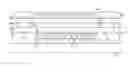
FIG. 1 shows a portion of an example electronic device 100. The electronic device 100 includes a semiconductor device package 102 and a circuit board 104, which may be a printed circuit board (PCB). The semiconductor device package 102 includes a semiconductor die 106 and a laminate layer 107, which is the substrate to which the die 106 is mounted.
The semiconductor die 106 includes an active side 108 and an inactive side 110 that is opposite the active side 108. The active side 108 is the side of the die 106 containing the active logic circuitry, such as semiconductor transistors. The inactive side 110, by comparison, does not include any active logic circuitry; likewise, the laminate layer 107 is devoid of active semiconductor circuitry. The semiconductor die 106 includes a number of TSVs 112 extending through the die 106 at the inactive side 110 beginning at inactive-side connection pads 111 and connecting to the active logic circuitry at the active side 108. The TSVs 112 thus conductively connect the active side 108 to the inactive side 110.
In the example of FIG. 1, the laminate layer 107 is mounted at a side thereof to the active side 108 of the semiconductor die 106 at active-side connection pads 109 via solder bumps 114, which may be controlled collapse chip connection (C4) solder bumps. In other implementations, solder bumps 114 are augmented or replaced by copper pillars or a flip-chip interconnection. It is also noted that the solder bumps 114 are depicted in simplified fashion in FIG. 1 and the other figures for illustrative convenience and clarity, and in actuality may be compressed as opposed to spherical as depicted in the figures. The semiconductor device package 102 includes conductive lands 116 at the other side of the laminate layer 107 by which another semiconductor device package can be mounted in a “package on package” manner, or by which another semiconductor die can be mounted in a “double sided chip” manner. The semiconductor device package 102 also includes solder balls 118 on the side of the laminate layer 107 at which the layer 107 is attached to the die 106, around the semiconductor die 106. The solder balls 118 may be ball grid array (BGA) solder balls, for instance. Not shown in FIG. 1 is that the laminate layer 107 can include connection pads at locations to which the solder balls 118 and/or the solder bumps 114 are to attach.
The circuit board 104 includes conductive lands 120 for conductively connecting the semiconductor device package 102. Specifically, the laminate layer 107 is directly connected to the circuit board 104 via the solder balls 118 connecting to corresponding conductive lands 120. The TSVs 112 of the semiconductor die 106 are directly connected to the circuit board 104 at the inactive-side connection pads 111 via solder paste 122, which may be screened solder paste. Therefore, in the example of FIG. 1, the circuit board 104 is mounted to the inactive side 110 of the die 106. It is noted that the solder paste 122 is depicted in simplified and larger fashion in FIG. 1 and the other figures for illustrative convenience and clarity, and in actuality may be smaller and/or compressed as opposed to larger and spherical as depicted in the figures. It is also noted that the connection pads 111 can be larger width-wise than the TSVs 112 as compared as in FIG. 1 and the other figures.
The logic circuitry at the active side 108 of the semiconductor die 106 performs functionality by receiving power, and by receiving input and/or providing output. As such, the semiconductor die 106 includes power/ground lines to receive power, and signal lines to receive input and/or provide output. The signal lines may be connected via the TSVs 112 to the circuit board 104 and the power/ground lines connected via the solder balls 118 and through the laminate layer 107 to the circuit board 104 in one implementation. In this respect, the laminate layer 107 provides for signal routing, although as noted above the layer 107 itself has no active logic circuitry.
In another implementation, the power/ground lines may be connected via the TSVs 112 and the signal lines via the solder balls 118 and through the laminate layer 107. In a different implementation, at least some signal lines may be connected via the TSVs 112 and other signal lines via the solder balls 118 and through the laminate layer 107. Similarly, in one implementation, at least some power/ground lines may be connected via the TSVs 112 and other power/ground lines via the solder balls 118 and through the laminate layer 107.
It is noted that there can be an underfill layer to either side of the semiconductor die 106. Thus, there can be one underfill layer encapsulating the area surrounding the solder paste 122 from the bottom of the semiconductor die 106 to the top of the circuit board 104, and another underfill layer encapsulating the area surrounding the solder bumps 114 from the top of die 106 to the bottom of the laminate layer 107. In another implementation, there can be a single underfill layer extending from the top of the circuit board 104 to the bottom of the laminate layer 107, encapsulating the solder paste 122, the semiconductor die 106, and the solder bumps 114.
FIG. 2 shows another example implementation of the electronic device 100. As in FIG. 1, the electronic device 100 in FIG. 2 includes the semiconductor device package 102 and the circuit board 104. Like-numbered parts of FIG. 2 are at least substantially identical in functionality as described with reference to FIG. 1, and their description with reference to FIG. 2 is omitted herein to avoid duplication. Furthermore, for illustrative clarity, certain components of FIG. 1 are omitted from FIG. 2 but can be present, such as the connection pads 109 and 111 and the conductive lands 116 and 120.
In FIG. 2, the electronic device 100 includes another semiconductor die 204 within an overmold layer 202. The overmold layer 202 is attached to the laminate layer 107 at the side of the layer 107 opposite the side at which the layer 107 is attached to the semiconductor die 106. The semiconductor die 204 can be conductively connected to (and thus through) the laminate layer 107 in a number of different ways to conductively expose the die 204 through the laminate layer 107. For instance, wirebonding within the overmold layer 202 can connect the die 204 to the laminate layer 107. As another example, the semiconductor die 204 can be disposed in a “flip chip” configuration to conductively connect to the laminate layer 107 via solder bumps within the overmold layer 202.
FIG. 3 shows a third example implementation of the electronic device 100. As in FIG. 1, the electronic device 100 in FIG. 3 includes the semiconductor device package 102 and the circuit board 104. Like-numbered parts of FIG. 3 are at least substantially identical in functionality as described with reference to FIG. 1, and their description with reference to FIG. 2 is omitted herein to avoid duplication. Furthermore, for illustrative clarity, certain components of FIG. 1 are omitted from FIG. 2 but can be present, such as the connection pads 109 and 111 and the conductive lands 116 and 120.
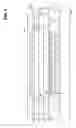
In FIG. 3, the electronic device 100 includes another semiconductor device package 302 mounted to the semiconductor device package 102 in a “package on package” configuration. The semiconductor device package 302 includes another semiconductor die 310 within an overmold layer 308, and a laminate layer 312. The semiconductor die 310 can be conductively connected to and through the laminate layer 312 via wirebonding within the overmold layer 308, via solder bumps within the overmold layer 308 when in a “flip chip” configuration, and so on, as has been described above with reference to FIG. 2.
In FIG. 3, the semiconductor device package 102 may include an overmold layer 304 that includes through-mold vias (TMVs) 306 to conductively connect the package 102 with the semiconductor device package 302 via solder balls 314. A third semiconductor die of the electronic device 100 can be included in the semiconductor device package 102, such that the semiconductor device package 102 can include two semiconductor dies as in FIG. 2 in one implementation. In another implementation, the third semiconductor die can be similar to the semiconductor die 106 and have TSVs to permit the semiconductor device package 102 to interconnect with the semiconductor device package 302 via solder bumps, in addition to via the solder balls 314 and the TMVs 306.
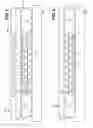
In the electronic device 100 in the example implementations of FIGS. 1, 2, and 3, the circuit board 104 connects to the inactive side 110 of the semiconductor die 106 of the semiconductor device package 102, whereas the active side 108 connects to the laminate layer 107 of the package 102. By comparison, FIG. 4 shows an example implementation of the electronic device 100 in which the circuit board 104 is connected to the active side 108 of the semiconductor die 106 of the semiconductor device package 102, and the inactive side 110 connects to the laminate layer 107 of the package 102. It is noted that the connection pads 109 and 111 and the conductive lands 116 and 120 are omitted from FIG. 4 for illustrative clarity and convenience, but can be present.
In FIG. 4, then, the circuit board 104 is mounted to the active side 108 of the semiconductor die 106 via the solder bumps 114. The laminate layer 107 is mounted to the TSVs 112 on the inactive side 110 of the semiconductor die 106 via the solder paste 122. The circuit board 104 is still mounted to the laminate layer 107 in FIG. 4 as in FIG. 2, via the solder balls 118. Thus, the circuit board 104 is conductively connected to the active side 108 of the semiconductor die 106 both directly (via the solder bumps 114) and indirectly (via the solder balls 118 and the laminate layer 107) in this implementation.
FIG. 5 shows an example method 500 for fabricating the electronic device of FIGS. 1, 2, 3, 4, and 5 that have been described. The semiconductor die 106 is first prepared (502). This includes thinning a semiconductor wafer including the die 106 and having the TSVs 112 embedded therein to expose the TSVs 112 (504), forming the connection pads 109 and 111 on the die 106 (506), and forming the solder bumps 114 at the active side 108 of the die 106 (508). Forming the connection pads 111 on the inactive side 110 can include forming a redistribution layer within which the pads 111 are formed.
In one implementation (e.g., FIGS. 1, 2, and 3), the active side 108 of the semiconductor die 106 is attached to the laminate layer 107, per part 510, whereas in another implementation (e.g., FIG. 4), the active side 108 is attached to the circuit board 104, per part 512. In the former implementation, first the laminate layer 107 is attached to the active side 108 of the semiconductor die 106 via the solder bumps 114 (514). Next, the circuit board 104 is attached to the inactive side 110 of the semiconductor die 106 via the solder paste 122 and to the laminate layer 107 via the solder balls 118 (516).
In the latter implementation, by comparison, first the circuit board 104 is attached to the active side 108 of the semiconductor die 106 via the solder bumps 114 (518). Next, the laminate layer 107 is attached to the semiconductor die 106 via the solder paste 122 and to the circuit board 104 via the solder balls 118 (516). Note that in both implementations, the laminate layer 107 and the circuit board 104 are attached to one another via the solder balls 118. In either implementation, another semiconductor die 204 within the semiconductor device package 102 can be attached as in FIG. 2, or another semiconductor device package 302 including another semiconductor die 310 can be attached as in FIG. 3 (522).
It is noted that, although specific embodiments have been illustrated and described herein, it will be appreciated by those of ordinary skill in the art that any arrangement calculated to achieve the same purpose may be substituted for the specific embodiments shown. This application is thus intended to cover any adaptations or variations of embodiments of the present invention. As such and therefore, it is manifestly intended that this invention be limited only by the claims and equivalents thereof.
Claims
We claim:1. A method comprising:
preparing a semiconductor die having an active side, an inactive side opposite the active side, and a plurality of through-silicon vias (TSVs) conductively connecting the active side to the inactive side;
attaching a laminate layer to the semiconductor die; and
attaching a circuit board to the semiconductor die.
2. The method of claim 1, wherein the laminate layer is attached to the semiconductor die before the circuit board is attached to the semiconductor die,
wherein attaching the laminate layer to the semiconductor die comprises employing a plurality of solder bumps to attach a side of the laminate layer to the active side of the semiconductor die,
and wherein attaching the circuit board to the semiconductor die includes attaching the circuit board to the laminate layer and comprises:
employing a plurality of solder balls at the side of the laminate layer attached to the semiconductor die, around the semiconductor die, to attach laminate layer to the circuit board; and
employing solder paste to attach the circuit board to the inactive side of the semiconductor at which the TSVs are exposed.
3. The method of claim 1, wherein the laminate layer is attached to the semiconductor die after the circuit board is attached to the semiconductor die,
wherein attaching the circuit board to the semiconductor die comprises employing a plurality of solder bumps to attach the circuit board to the active side of the semiconductor die,
and wherein attaching the laminate layer to the semiconductor die includes attaching the laminate layer to the circuit board and comprises:
employing solder paste to attach a side the laminate layer to the inactive side of the semiconductor die at which the TSVs are exposed; and
employing a plurality of solder balls at the side of the laminate layer, around the semiconductor die, to attach the laminate layer to the circuit board.
4. The method of claim 1, wherein preparing the semiconductor die comprises:
thinning a semiconductor wafer including the semiconductor die and having the TSVs embedded therein to expose the TSVs;
forming a plurality of connection pads at the inactive side of the semiconductor die; and
forming a plurality of solder bumps at the active side of the semiconductor die.
5. The method of claim 4, wherein forming the connection pads at the inactive side comprises forming a redistribution layer within which the connection pads are formed.
6. The method of claim 1, wherein the semiconductor die is a first semiconductor die attached to a first side of the laminate layer, and the method further comprises:
attaching one or more of a second semiconductor die and a second semiconductor package to a second side of the laminate layer opposite the first side.
Images & Drawings included:
Sources:
- United States Patent and Trademark Office - verify current appl. status at the USPTO↗
Similar patent applications:
Recent applications in this class:
- » 20250273622 2025-08-28
ELECTRONIC PACKAGE AND MANUFACTURING METHOD THEREOF - » 20250266391 2025-08-21
LASER ASSISTED BONDING METHOD - » 20250259964 2025-08-14
MOLDED SPACER FOR SURFACE MOUNT TECHNOLOGY - » 20250246576 2025-07-31
ELECTRONIC DEVICE AND A METHOD FOR FORMING THE SAME - » 20250226358 2025-07-10
PRE-ATTACHED ENGINEERED SOLDERS FOR ULTRA-LOW RESIDUE SOLDERING - » 20250226357 2025-07-10
ELECTRICAL CIRCUIT FORMATION METHOD AND ELECTRICAL CIRCUIT FORMATION DEVICE - » 20250219019 2025-07-03
SEMICONDUCTOR DEVICE AND METHOD FOR MANUFACTURING THE SAME - » 20250219018 2025-07-03
SEMICONDUCTOR PACKAGING METHOD, SEMICONDUCTOR ASSEMBLY COMPONENT AND ELECTRONIC DEVICE - » 20250219017 2025-07-03
DIE-BONDING METHOD FOR PREVENTING DIE FROM BENDING - » 20250210584 2025-06-26
METHOD OF BONDING LIGHT EMITTING ELEMENT AND METHOD OF MANUFACTURING DISPLAY DEVICE, HAVING THE SAME
Recent applications for this Assignee:
- » 20250294045 2025-09-18
THREAT POLICY FINE-TUNING BASED ON THE VULNERABILITY OF A SUBNET AS A SOURCE OF A MALICIOUS ATTACK - » 20250294041 2025-09-18
DEVICE POPULATION ANOMALY DETECTION - » 20250292574 2025-09-18
SCENE PARSING - » 20250292026 2025-09-18
A GENERATIVE ARTIFICIAL INTELLIGENCE COMMENTARY - » 20250291689 2025-09-18
MACHINE LEARNING MODEL TRAINING TO ASSIST IN SYSTEM DEBUG - » 20250287215 2025-09-11
PORTABLE MEDIA GEOFENCE AND DEVICE PAIRING SECURITY - » 20250285610 2025-09-11
RECIPIENT-SPECIFIC VOICE TONE ADJUSTMENT IN TELEPHONY - » 20250284728 2025-09-11
CONTEXT LARGE LANGUAGE MODEL OUTPUT EXPLANATION - » 20250278669 2025-09-04
COUNTERFACTUALS WITH FEATURE PREFERENCES FOR CONSISTENT AND DIVERSE EXPLANATIONS - » 20250274345 2025-08-28
MULTI-LAYER EDGE ARCHITECTURE SIMULATION