Semiconductor device and method for fabricating the same
US20160079173A1
2016-03-17
14/489,461
2014-09-17
✅ Patent granted
US 9,870,994 B2
2018-01-16
-
-
Peniel M Gumedzoe | Christopher Johnson
Winston Hsu
2034-09-17
Abstract:
A method for fabricating semiconductor device is disclosed. The method includes the steps of: providing a substrate; forming an ultra low-k (ULK) dielectric layer on the substrate; forming a hard mask on the ULK dielectric layer; forming an opening in the hard mask and the ULK dielectric layer; forming a conductive layer in the opening and on the hard mask; planarizing the conductive layer; and removing the hard mask to expose the ULK dielectric layer so that the top surface of the ULK dielectric layer is lower than the top surface of the conductive layer.
Assignee:
- UNITED MICROELECTRONICS CORP. 2,360 🇹🇼 Hsin-Chu, Taiwan
Applicant:
Interested in similar patents?
Get notified when new applications in this technology area are published.
Classification:
H01L23/53209 » CPC further
Details of semiconductor or other solid state devices; Arrangements for conducting electric current within the device in operation from one component to another, i.e. interconnections, e.g. wires, lead frames including external interconnections consisting of a multilayer structure of conductive and insulating layers inseparably formed on the semiconductor body characterised by the materials; Conductive materials based on metals, e.g. alloys, metal silicides
H01L23/5329 » CPC further
Details of semiconductor or other solid state devices; Arrangements for conducting electric current within the device in operation from one component to another, i.e. interconnections, e.g. wires, lead frames including external interconnections consisting of a multilayer structure of conductive and insulating layers inseparably formed on the semiconductor body characterised by the materials Insulating materials
H01L21/76802 » CPC further
Processes or apparatus adapted for the manufacture or treatment of semiconductor or solid state devices or of parts thereof; Manufacture or treatment of devices consisting of a plurality of solid state components formed in or on a common substrate or of parts thereof; Manufacture of integrated circuit devices or of parts thereof; Manufacture of specific parts of devices defined in group; Applying interconnections to be used for carrying current between separate components within a device comprising conductors and dielectrics characterised by the formation and the after-treatment of the dielectrics, e.g. smoothing by forming openings in dielectrics
H01L21/76877 » CPC further
Processes or apparatus adapted for the manufacture or treatment of semiconductor or solid state devices or of parts thereof; Manufacture or treatment of devices consisting of a plurality of solid state components formed in or on a common substrate or of parts thereof; Manufacture of integrated circuit devices or of parts thereof; Manufacture of specific parts of devices defined in group; Applying interconnections to be used for carrying current between separate components within a device comprising conductors and dielectrics characterised by the formation and the after-treatment of the conductors Filling of holes, grooves or trenches, e.g. vias, with conductive material
H01L21/7684 » CPC further
Processes or apparatus adapted for the manufacture or treatment of semiconductor or solid state devices or of parts thereof; Manufacture or treatment of devices consisting of a plurality of solid state components formed in or on a common substrate or of parts thereof; Manufacture of integrated circuit devices or of parts thereof; Manufacture of specific parts of devices defined in group; Applying interconnections to be used for carrying current between separate components within a device comprising conductors and dielectrics characterised by the formation and the after-treatment of the conductors Smoothing; Planarisation
H01L21/76843 » CPC further
Processes or apparatus adapted for the manufacture or treatment of semiconductor or solid state devices or of parts thereof; Manufacture or treatment of devices consisting of a plurality of solid state components formed in or on a common substrate or of parts thereof; Manufacture of integrated circuit devices or of parts thereof; Manufacture of specific parts of devices defined in group; Applying interconnections to be used for carrying current between separate components within a device comprising conductors and dielectrics characterised by the formation and the after-treatment of the conductors; Barrier, adhesion or liner layers formed in openings in a dielectric
H01L21/0332 » CPC further
Processes or apparatus adapted for the manufacture or treatment of semiconductor or solid state devices or of parts thereof; Manufacture or treatment of semiconductor devices or of parts thereof; Making masks on semiconductor bodies for further photolithographic processing not provided for in group or comprising inorganic layers characterised by their composition, e.g. multilayer masks, materials
H01L21/02 IPC
Processes or apparatus adapted for the manufacture or treatment of semiconductor or solid state devices or of parts thereof Manufacture or treatment of semiconductor devices or of parts thereof
H01L21/033 IPC
Processes or apparatus adapted for the manufacture or treatment of semiconductor or solid state devices or of parts thereof; Manufacture or treatment of semiconductor devices or of parts thereof; Making masks on semiconductor bodies for further photolithographic processing not provided for in group or comprising inorganic layers
H01L23/528 » CPC further
Details of semiconductor or other solid state devices; Arrangements for conducting electric current within the device in operation from one component to another, i.e. interconnections, e.g. wires, lead frames including external interconnections consisting of a multilayer structure of conductive and insulating layers inseparably formed on the semiconductor body layout of the interconnection structure
H01L21/76834 » CPC further
Processes or apparatus adapted for the manufacture or treatment of semiconductor or solid state devices or of parts thereof; Manufacture or treatment of devices consisting of a plurality of solid state components formed in or on a common substrate or of parts thereof; Manufacture of integrated circuit devices or of parts thereof; Manufacture of specific parts of devices defined in group; Applying interconnections to be used for carrying current between separate components within a device comprising conductors and dielectrics characterised by the formation and the after-treatment of the dielectrics, e.g. smoothing characterised by the formation of thin functional dielectric layers, e.g. dielectric etch-stop, barrier, capping or liner layers formation of thin insulating films on the sidewalls or on top of conductors
H01L23/532 IPC
Details of semiconductor or other solid state devices; Arrangements for conducting electric current within the device in operation from one component to another, i.e. interconnections, e.g. wires, lead frames including external interconnections consisting of a multilayer structure of conductive and insulating layers inseparably formed on the semiconductor body characterised by the materials
H01L21/768 IPC
Processes or apparatus adapted for the manufacture or treatment of semiconductor or solid state devices or of parts thereof; Manufacture or treatment of devices consisting of a plurality of solid state components formed in or on a common substrate or of parts thereof; Manufacture of integrated circuit devices or of parts thereof; Manufacture of specific parts of devices defined in group Applying interconnections to be used for carrying current between separate components within a device comprising conductors and dielectrics
H01L21/76885 » CPC further
Processes or apparatus adapted for the manufacture or treatment of semiconductor or solid state devices or of parts thereof; Manufacture or treatment of devices consisting of a plurality of solid state components formed in or on a common substrate or of parts thereof; Manufacture of integrated circuit devices or of parts thereof; Manufacture of specific parts of devices defined in group; Applying interconnections to be used for carrying current between separate components within a device comprising conductors and dielectrics characterised by the formation and the after-treatment of the conductors By forming conductive members before deposition of protective insulating material, e.g. pillars, studs
H01L2924/0002 » CPC further
Indexing scheme for arrangements or methods for connecting or disconnecting semiconductor or solid-state bodies as covered by; Technical content checked by a classifier Not covered by any one of groups , and
Description
BACKGROUND OF THE INVENTION
1. Field of the Invention
The invention relates to a method for fabricating semiconductor device, and more particularly, to a method of preventing damages to low-k dielectric films during fabrication of metal interconnections.
2. Description of the Prior Art
Integrated circuits have evolved into complex devices that can include millions of components (e.g., transistors, capacitors and resistors) on a single chip. The demand for greater circuit density necessitates a reduction in the dimensions of the integrated circuit components, e.g., sub-micron dimensions and the use of various materials to fabricate devices in order to achieve much faster and better electrical performance, such as materials with higher conductivity used in metal lines, materials with lower permittivity (low-k) dielectric constant used as insulating materials, etc. For integrated circuit fabrication, metal interconnects with low resistance, such as copper and aluminum interconnects, provide conductive paths between the integrate circuit components on integrated circuit devices. Generally, metal interconnects are electrically isolated from each other by a dielectric bulk insulating material. At sub-micron dimensions, capacitive coupling potentially occurs between adjacent metal interconnects, which may cause cross talk and/or resistance-capacitance (RC) delay and degrade the overall performance of the integrated circuit.
One method for forming vertical and horizontal interconnects for the integrated circuit components is by a damascene or dual damascene method. Typically, damascene structures have dielectric bulk insulating layers and conductive metal layers, such as low dielectric constant materials and conductive copper layers, stacked on top of one another. Vertical interconnects, i.e., vias, and horizontal interconnects, i.e., trenches are etched into the dielectric bulk insulating layer and the conductive metal layers are subsequently filled into the vias and/or trenches and planarized, such as by a chemical mechanical planarization process (CMP), so that the conducting metal materials are only left in the vias and/or trenches. In the damascene approach, a rather complex dielectric film stack that includes a sequence of hard mask, low-k dielectrics, and etch stop layers, etc., may be required. To obtain such a stack, via/trench lithography, patterning, and wet cleanings are typically required before filing the vias and the trenches with the conductive metal materials.
However, low-k materials of the damascene structure are susceptible to various damages during subsequent processing steps, such as etching, wet-cleaning, pre-metal cleaning, or CMP etc. Such damages can severely increase the dielectric constant of the low-k materials, causing the overall dielectric constant of the resulting dielectric film stack to increase. Therefore, there is a need for a process of making damascene structures with zero or minimized damages to low-k materials in the dielectric film stack.
SUMMARY OF THE INVENTION
According to a preferred embodiment of the present invention, a method for fabricating semiconductor device is disclosed. The method includes the steps of: providing a substrate; forming an ultra low-k (ULK) dielectric layer on the substrate; forming a hard mask on the ULK dielectric layer; forming an opening in the hard mask and the ULK dielectric layer; forming a conductive layer in the opening and on the hard mask; planarizing the conductive layer; and removing the hard mask to expose the ULK dielectric layer so that the top surface of the ULK dielectric layer is lower than the top surface of the conductive layer.
According to another aspect of the present invention, a semiconductor device is disclosed. The semiconductor device includes: a substrate; an ULK dielectric layer on the substrate; a conductive layer embedded in the ULK dielectric layer, wherein the top surface of the ULK dielectric layer is lower than the top surface of the conductive layer; and a cap layer on the conductive layer while contacting the ULK dielectric layer directly, in which the top surface of the cap layer on the ULK dielectric layer is higher than the top surface of the conductive layer.
These and other objectives of the present invention will no doubt become obvious to those of ordinary skill in the art after reading the following detailed description of the preferred embodiment that is illustrated in the various figures and drawings.
BRIEF DESCRIPTION OF THE DRAWINGS
FIGS. 1-5 illustrate a method for fabricating semiconductor device according to a preferred embodiment of the present invention.
FIG. 6, which illustrates another approach for fabricating semiconductor device according to an embodiment of the present invention.
FIGS. 7-8 illustrate another approach for fabricating semiconductor device according to an embodiment of the present invention.
DETAILED DESCRIPTION
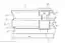
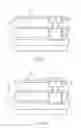
Referring to FIGS. 1-5, FIGS. 1-5 illustrate a method for fabricating semiconductor device according to a preferred embodiment of the present invention. As shown in FIG. 1, a substrate 12 is provided, in which the substrate 12 could be composed of monocrystalline silicon, gallium arsenide (GaAs) or other known semiconductor material. The substrate 12 could also include fin-shaped structures and shallow trench isolation structures (STIs) surrounding the fin-shaped structures. A standard metal-oxide semiconductor (MOS) transistor fabrication could be performed to form at least one MOS transistor (not shown) or other semiconductor devices on the substrate, in which the MOS transistor could be a PMOS transistor, NMOS transistor, or CMOS transistor, and the MOS transistor could also include typical transistor structures including metal gate, spacer, source/drain regions, epitaxial layers, and/or silicides.
After forming the MOS transistor on the substrate 12, an interlayer dielectric (ILD) layer 14 is covered on the substrate 12 and the MOS transistor, a contact plug 16 is formed in the ILD 14 layer, and an a plurality of dielectric layers and metal interconnections are formed atop the ILD layer. In this embodiment, a cap layer 18 such as an organic dielectric coating (ODC) and an ultra low-k (ULK) dielectric layer 20 are formed on the ILD layer 14, and a trench conductor 22 with barrier layer 24 around is formed in the cap layer 18 and ULK dielectric layer 20 through typical metal interconnective or damascene processes.
Another cap layer 26 such as a nitrogen-doped carbon (NDC) material layer, another ULK dielectric layer 28, a hard mask 30 and another hard mask such as a metal layer 32 are formed on the ULK dielectric layer 20 thereafter, and a damascene process could be carried out to first remove part of metal layer 32, part of the hard mask 30, part of the ULK dielectric layer 28, and part of the cap layer 26 for forming an opening (not shown), and a barrier layer 34 and a conductive layer 36 are deposited in the opening. Preferably, the thickness of the hard mask 30 is preferably between 20-150 Angstroms, the hard mask 30 is composed of SiON, the metal layer 32 is composed of TiN, the barrier layer 34 is composed of Ta, Ti, TaN, or TiN, and the conductive layer 36 is composed of Cu, but not limited thereto.
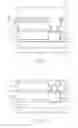
Next, as shown in FIG. 2, a planarizing process, such as a chemical mechanical polishing (CMP) process is conducted to remove part of the conductive layer 36, all of the barrier layer 34 on the ULK dielectric layer 28, and all of the metal layer 32 to expose the top surface of the hard mask 30, so that the top surface of the hard mask 30 is preferably even with the top surface of the conductive layer 36.
Next, as shown in FIG. 3, an etching back process is conducted to fully remove the hard mask 30 for exposing the ULK dielectric layer 28 underneath so that while part of the conductive layer 36 is embedded in the ULK dielectric layer 28, the top surface of the ULK dielectric layer 28 is lower than the top surface of the conductive layer 36. Preferably, by using an additional etching back process to remove the hard mask 30 separately before exposing the ULK dielectric layer 28, the present invention could reduce the damage done to ULK dielectric layer 28 if both the metal layer 32 and hard mask 30 were planarized by CMP process to expose the ULK dielectric layer 28 directly.
Next, as shown in FIG. 4, a metal layer 38 is formed on the conductive layer 36 after removing the hard mask 30. In this embodiment, metal layer 38 is composed of CuMn, CoW, Co, or CoWP
Next, as shown in FIG. 5, a cap layer 40 is formed on the ULK dielectric layer 28 and the metal layer 38, in which the cap layer 40 could be composed of SiN, SiON, SiC, SiCON, SiCO, or SiCN. The thickness of the cap layer 40 is preferably between 100-300 Angstroms. From a structural view, the cap layer 40 is formed on the conductive layer 36 and metal layer 38 while contacting the ULK dielectric layer 28 directly, in which the top surface of the cap layer 40 on the ULK dielectric layer 28 is higher than the top surface of the conductive layer 36 and also higher than the top surface of the metal layer 38, or the top surface of the portion of the cap layer 40 directly contacting the ULK layer 28 is higher than the top surface of the conductive layer 36. This completes the fabrication of a semiconductor device according to a preferred embodiment of the present invention.
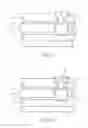
Referring to FIG. 6, which illustrates another approach for fabricating semiconductor device according to an embodiment of the present invention. As shown in FIG. 6, instead of removing the hard mask 30 without damaging the barrier layer 34 as revealed in FIG. 3, it would be desirable to remove the hard mask 30 and part of the barrier layer 34 simultaneously while the hard mask 30 is fully removed by a dry etching process. Nevertheless, it should be noted that while part of barrier layer 34 is removed along with the hard mask 30, the tip of the barrier layer 34 would not be even with the top surface of the ULK dielectric layer 28. Instead, the tip of the barrier layer 34 would be slightly above the top surface of the ULK dielectric layer.
As the hard mask 30 and part of the barrier layer 34 are removed, the ULK dielectric layer 28 and sidewalls of the conductive layer 36 are exposed simultaneously. Next, a metal layer 38 could be deposited and since the top surface and sidewalls of the conductive layer 36 are both exposed at this stage, the metal layer 38 is preferably formed to cover the top surface and sidewalls of the conductive layer 36. Consequently, a reversed U-shaped metal layer 38 would be formed on the conductive layer 36 and in this instance, the top surface of the ULK dielectric layer 28 would be lower than the top of the barrier layer 34 and bottom of the metal layer 38. A cap layer 40 could be formed on the ULK dielectric layer 28 and the metal layer 38 thereafter. Similar to the aforementioned embodiment, the metal layer 38 could be composed of CuMn, CoW, Co, or CoWP, and the cap layer 40 could be composed of SiN, SiON, SiC, or SiCN, but not limited thereto.
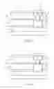
Referring to FIGS. 7-8, FIGS. 7-8 illustrate another approach for fabricating semiconductor device according to an embodiment of the present invention. As shown in FIG. 7, instead of removing the hard mask 30 completely before forming the metal layer 38 as disclosed in FIGS. 3-4, it would also be desirable to fully remove the hard mask 30 after the metal layer 38 is formed. For instance, after forming the hard mask 30 as shown in FIG. 2, a metal layer 38 could be formed atop the conductive layer 36 while the hard mask 30 is still on the ULK dielectric layer 28, as shown in FIG. 7. Next, as shown in FIG. 8, the hard mask 30 is then removed through an etching back process to expose the ULK dielectric layer 28 and a cap layer 40 is formed on the ULK dielectric layer 28 and the metal layer 38.
Those skilled in the art will readily observe that numerous modifications and alterations of the device and method may be made while retaining the teachings of the invention. Accordingly, the above disclosure should be construed as limited only by the metes and bounds of the appended claims.
Claims
1. A method for fabricating semiconductor device, comprising:
providing a substrate;
forming an ultra low-k (ULK) dielectric layer on the substrate;
forming a hard mask on the ULK dielectric layer;
forming an opening in the hard mask and the ULK dielectric layer;
forming a conductive layer in the opening and on the hard mask;
planarizing the conductive layer; and
removing the hard mask to expose the ULK dielectric layer so that the top surface of the ULK dielectric layer is lower than the top surface of the conductive layer.
2. The method of claim 1, further comprising forming a metal layer on the conductive layer after removing the hard mask.
3. The method of claim 2, wherein the metal layer comprises CuMn, CoW, Co, or CoWP.
4. The method of claim 2, further comprising forming a cap layer on the ULK dielectric layer and the metal layer.
5. The method of claim 1, further comprising removing the hard mask after forming a metal layer on the conductive layer.
6. The method of claim 5, wherein the metal layer comprises CuMn, CoW, Co, or CoWP.
7. The method of claim 5, further comprising forming a cap layer on the ULK dielectric layer and the metal layer.
8. The method of claim 1, wherein the conductive layer comprises copper.
9. The method of claim 1, further comprising:
forming a barrier layer and the conductive layer in the opening and on the hard mask;
planarizing the conductive layer and the barrier layer;
removing the hard mask and the barrier layer to expose the ULK dielectric layer and sidewalls of the conductive layer;
forming a metal layer on the top surface and sidewalls of the conductive layer; and
forming a cap layer on the ULK dielectric layer and the metal layer.
10. The method of claim 9, wherein the cap layer comprises SiCN, SiCON, or SiCO.
11. The method of claim 1, wherein the hard mask comprises SiON.
12. A semiconductor device, comprising:
a substrate;
an ULK dielectric layer on the substrate;
a conductive layer embedded in the ULK dielectric layer, wherein the top surface of the ULK dielectric layer is lower than the top surface of the conductive layer;
a metal layer on the conductive layer; and
a cap layer on the conductive layer while contacting the ULK dielectric layer directly, wherein the top surface of the cap layer on the ULK dielectric layer is higher than the top surface of the metal layer.
13. (canceled)
14. The semiconductor device of claim 12, wherein the metal layer comprises CuMn, CoW, Co, or CoWP.
15. The semiconductor device of claim 12, wherein the conductive layer comprises copper.
16. The semiconductor device of claim 12, further comprising:
the metal layer on top surface and sidewalls of the conductive layer;
a barrier layer between the conductive layer and the ULK dielectric layer and contacting the metal layer; and
the cap layer on the ULK dielectric layer and the metal layer.
17. The semiconductor device of claim 16, wherein the metal layer comprises CuMn, CoW, Co, or CoWP.
18. The semiconductor device of claim 16, wherein the top surface of the ULK dielectric layer is lower than the top of the barrier layer and bottom of the metal layer.
19. The semiconductor device of claim 12, wherein the cap layer comprises SiCN, SiCON, or SiCO.
20. (canceled)
Images & Drawings included:
Sources:
- United States Patent and Trademark Office - verify current appl. status at the USPTO↗
Similar patent applications:
- » 20120112209
SILICON CARBIDE SUBSTRATE FABRICATION METHOD, SEMICONDUCTOR DEVICE FABRICATION METHOD, SILICON CARBIDE SUBSTRATE, AND SEMICONDUCTOR DEVICE - » 20080315254
Semiconductor device fabrication method, semiconductor device, and semiconductor layer formation method - » 20060043570
Substrate, semiconductor device, substrate fabricating method, and semiconductor device fabricating method - » 20050014377
Semiconductor device fabrication method and semiconductor device fabrication system for minimizing film-thickness variations - » 20080203440
Semiconductor device fabrication method and semiconductor device fabricated thereby - » 10129305
Semiconductor device fabrication method and semiconductor device fabrication apparatus - » 20060118952
Micro-hole plating method, gold bump fabrication method and semiconductor device fabrication method using the micro-hole plating method, semiconductor device - » 10107298
Semiconductor device fabrication method and semiconductor device - » 20060084251
Plating method, semiconductor device fabrication method and circuit board fabrication method - » 20060084253
Plating method, semiconductor device fabrication method and circuit board fabrication method
Recent applications in this class:
- » 20250279364 2025-09-04
VIA FOR SEMICONDUCTOR DEVICE AND METHOD - » 20250210524 2025-06-26
MULTI-LAYER LINE STRUCTURE - » 20250201716 2025-06-19
TANTALUM ELECTRODE WITH TANTALUM NITRIDE LINER AS RIE DIFFUSION BARRIER - » 20250192052 2025-06-12
GRAPHENE LINERS AND CAPS FOR SEMICONDUCTOR STRUCTURES - » 20250140696 2025-05-01
INTERCONNECTION STRUCTURE AND MANUFACTURING METHOD THEREOF - » 20250112157 2025-04-03
SYSTEM AND METHODS FOR A METAL INTERFACE ARCHITECTURE - » 20250112156 2025-04-03
BARRIER LAYERS FOR INTERCONNECTS - » 20250079313 2025-03-06
SEMICONDUCTOR STRUCTURE AND MANUFACTURING METHOD THEREOF - » 20250079312 2025-03-06
METHODS AND STRUCTURES FOR HIGH STRENGTH DIELECTRIC IN HYBRID BONDING - » 20250046716 2025-02-06
MODIFIED REVERSE SELECTIVE BARRIER STRUCTURE
Recent applications for this Assignee:
- » 20250173280 2025-05-29
Interconnects for physically unclonable function and method of achieving physically unclonable function through interconnects - » 20250142801 2025-05-01
Layout pattern for static random access memory - » 20250120092 2025-04-10
MRAM STRUCTURE AND FABRICATING METHOD OF THE SAME - » 20250107114 2025-03-27
METAL-OXIDE-SEMICONDUCTOR CAPACITOR STRUCTURE - » 20250061944 2025-02-20
MEMORY CONTROL CIRCUIT CAPABLE OF GENERATING AN UPDATED REFERENCE CURRENT - » 20250014637 2025-01-09
MEMORY CIRCUIT - » 20240415024 2024-12-12
MAGNETORESISTIVE RANDOM ACCESS MEMORY DEVICE AND METHOD FOR FABRICATING THE SAME - » 20240355920 2024-10-24
HIGH ELECTRON MOBILITY TRANSISTOR AND METHOD FOR FORMING THE SAME - » 20240355894 2024-10-24
MANUFACTURING METHOD OF SEMICONDUCTOR DEVICE - » 20240355887 2024-10-24
Manufacturing method of semiconductor device