RESPONSE VALIDATION MECHANISM FOR TRIGGERING NON-INVASIVE RE-TEST ACCESS OF INTEGRATED CIRCUITS
US20160117261A1
2016-04-28
14/279,538
2014-05-16
Abstract:
In an embodiment of the invention, response validation offers increased integrated circuit security by using a unique password or re-test key for every integrated circuit manufactured. Non-invasive re-test of an IC can be performed using an encryption input.
Assignee:
- TEXAS INSTRUMENTS INCORPORATED 16,455 🇺🇸 Dallas, TX, United States
Interested in similar patents?
Get notified when new applications in this technology area are published.
Classification:
G06F12/1408 » CPC main
Accessing, addressing or allocating within memory systems or architectures; Protection against unauthorised use of memory or access to memory by using cryptography
H04L9/0822 » CPC further
arrangements for secret or secure communications Cryptographic mechanisms or cryptographic ; Network security protocols; Key distribution or management, e.g. generation, sharing or updating, of cryptographic keys or passwords; Key establishment, i.e. cryptographic processes or cryptographic protocols whereby a shared secret becomes available to two or more parties, for subsequent use; Key transport or distribution, i.e. key establishment techniques where one party creates or otherwise obtains a secret value, and securely transfers it to the other(s) using key encryption key
G06F11/2247 » CPC further
Error detection; Error correction; Monitoring; Detection or location of defective computer hardware by testing during standby operation or during idle time, e.g. start-up testing Verification or detection of system hardware configuration
G06F2212/1052 » CPC further
Indexing scheme relating to accessing, addressing or allocation within memory systems or architectures; Providing a specific technical effect Security improvement
G06F12/14 IPC
Accessing, addressing or allocating within memory systems or architectures Protection against unauthorised use of memory or access to memory
G06F11/22 IPC
Error detection; Error correction; Monitoring Detection or location of defective computer hardware by testing during standby operation or during idle time, e.g. start-up testing
H04L9/30 » CPC further
arrangements for secret or secure communications Cryptographic mechanisms or cryptographic ; Network security protocols Public key, i.e. encryption algorithm being computationally infeasible to invert or user's encryption keys not requiring secrecy
H04L9/08 IPC
arrangements for secret or secure communications Cryptographic mechanisms or cryptographic ; Network security protocols Key distribution or management, e.g. generation, sharing or updating, of cryptographic keys or passwords
Description
BACKGROUND
Integrated circuits (IC) are not always produced by companies that design or sell them. Anyone with access to a manufacturing process for integrated circuits could, in theory, introduce some change to the final IC. For complex ICs, small changes can have large effects and these changes can be difficult to detect. The threat of design alteration can be especially relevant to government agencies. Resolving doubt about IC integrity is one way to reduce technology vulnerabilities in military, finance, energy and political sectors of an economy. Since fabrication of integrated circuits in untrustworthy factories may occur, encryption and detection techniques are needed to verify the origin of manufacturing of the IC.
BRIEF DESCRIPTION OF THE DRAWINGS
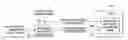
FIG. 1 is a block diagram illustrating a high level description of a response generation according to an embodiment of the invention.
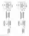
FIG. 2 is a block diagram illustrating a high level description of a response validation according to an embodiment of the invention.
DETAILED DESCRIPTION
In an embodiment of the invention, response validation offers increased device (IC) security by using a unique password or re-test key for every integrated circuit manufactured. Non-invasive re-test of an IC can be performed using an encryption input.
FIG. 1 is a block diagram illustrating a high level description of a response generation according to an embodiment of the invention. An encryption key 112 and a device specific encryption input 108 are input to an encryption algorithm 102. The device specific encryption input 108 is a unique value available or generated within the device 104 or externally. The encryption key 112 is a secret key that is generated for a specific family of integrated circuits. The stored response 110 generated by the encryption algorithm 102 is stored in secure non-volatile memory (NVM) 106 along with the device specific encryption input 108.
FIG. 2 is a block diagram illustrating a high level description of a response validation according to an embodiment of the invention. The encryption key 112 and a device read encryption input 208 (read from the NVM 106) are input to an encryption algorithm 102. When the device read encryption input 208 and the encryption key are valid, the encryption algorithm 102 inputs a validate response 210 into the device 104. After the validate response has been received by the device 104, the device 104 may be retested.
Claims
What is claimed is:1. A method for triggering non-invasive re-test access of an integrated circuit comprising:
providing an encryption key to a first input of an encryption algorithm;
providing a device specific encryption value to a second input of the encryption algorithm;
wherein the encryption algorithm provides a stored response, the stored response determined by the encryption key and the device specific encryption value;
electronically storing the stored response in a non-volatile memory (NVM) on the integrated circuit;
electronically storing the device specific encryption value in the NVM on the integrated circuit;
providing the encryption key to the first input of the encryption algorithm;
reading the device read encryption input from the NVM into the second input of the encryption algorithm;
providing a validate response to the integrated circuit when the encryption algorithm verifies that the read encryption key and the device read encryption input are valid; and
retesting the integrated circuit.
2. The method of claim 1 wherein the device specific encryption value is generated external to the integrated circuit.
3. The method of claim 1 wherein the device specific encryption value is generated on the integrated circuit.
Images & Drawings included:
Sources:
- United States Patent and Trademark Office - verify current appl. status at the USPTO↗
Recent applications in this class:
- » 20250165408 2025-05-22
TECHNIQUES AND DEVICES FOR CONFIGURABLE MEMORY ENCRYPTION AND AUTHENTICATION - » 20250165407 2025-05-22
MANAGING DATA SECURITY IN STORAGE DEVICES - » 20250156339 2025-05-15
NAMESPACE ENCRYPTION IN NON-VOLATILE MEMORY DEVICES - » 20250156338 2025-05-15
DATA INTEGRITY PROTECTION FOR RELOCATING DATA IN A MEMORY SYSTEM - » 20250156337 2025-05-15
MEMORY DEVICE WITH CRYPTOGRAPHIC KILL SWITCH - » 20250139020 2025-05-01
INFORMATION PROCESSING METHOD, CHIP, ELECTRONIC DEVICE, AND COMPUTER-READABLE STORAGE MEDIUM - » 20250130956 2025-04-24
COMPUTER SYSTEM AND METHOD FOR SYSTEM MEMORY ENCRYPTION AND DECRYPTION - » 20250103514 2025-03-27
TECHNOLOGIES FOR SECURE DEVICE CONFIGURATION AND MANAGEMENT - » 20250103513 2025-03-27
NONVOLATILE MEMORY DEVICE AND MEMORY SYSTEM - » 20250103512 2025-03-27
CACHE SCRUBBER CIRCUIT FOR CACHE-SET RANDOMIZATION TO RESIST CONTENTION-BASED CACHE ATTACKS
Recent applications for this Assignee:
- » 20250176083 2025-05-29
THREE LEVEL SWITCHING CONVERTER AND CONTROL - » 20250168790 2025-05-22
NODE SYNCHRONIZATION FOR NETWORKS - » 20250168096 2025-05-22
ADAPTIVE TIME SLOT ALLOCATION TO REDUCE LATENCY AND POWER CONSUMPTION IN A TIME SLOTTED CHANNEL HOPPING WIRELESS COMMUNICATION NETWORK - » 20250147310 2025-05-08
COMPACT NEAR EYE DISPLAY ENGINE - » 20250131264 2025-04-24
ON-CHIP TRAINING OF MACHINE LEARNING MODEL - » 20250125203 2025-04-17
CANTILEVERED DIES IN CERAMIC PACKAGES - » 20250119112 2025-04-10
Micro-Mechanical Resonator Having Out-of-Phase and Out-of-Plane Flexural Mode Resonator Portions - » 20250116702 2025-04-10
CLOCK SYNCHRONIZATION CIRCUIT - » 20250113548 2025-04-03
CARBON NANOTUBE DEVICES - » 20250105855 2025-03-27
PROGRAMMABLE GAIN AMPLIFIER AND A DELTA SIGMA ANALOG-TO-DIGITAL CONVERTER CONTAINING THE PGA