Light-Emitting Diode
US20160118540A1
2016-04-28
14/735,513
2015-06-10
Abstract:
A light-emitting diode includes at least an N-type layer, a light-emitting layer and a P-type layer, wherein the light-emitting layer forms a “V”-shaped indentation or pit during epitaxial process and the V pit is filled in with at least one type of metal nanoparticles to generate surface plasma coupling effect and to improve recombination probability of holes and electrons, thus improving internal quantum efficiency; further, a V pit is generated in the N-type layer during epitaxial process; surface plasma coupling effect is generated by filling metal nanoparticles in the V pit to increase light reflection, light extraction efficiency and external quantum efficiency, thereby improving light emitting efficiency of LED; and the V pit is formed directly by adjusting growth rate, thickness, temperature, pressure or doping during epitaxial process instead of etching, which causes no damage to the LED epitaxial layer, thus simplifying process and improving device stability.
Inventors:
- MU-SEN DONG 1 🇨🇳 Tianjin, China
- LI-YING SHEN 1 🇨🇳 Tianjin, China
- DU-XIANG WANG 5 🇨🇳 Tianjin, China
- CHAO-YU WU 1 🇨🇳 Tianjin, China
- LIANG-JUN WANG 3 🇨🇳 Tianjin, China
Assignee:
- TIANJIN SANAN OPTOELECTRONICS CO., LTD. 22 🇨🇳 Tianjin, China
Interested in similar patents?
Get notified when new applications in this technology area are published.
Classification:
H01L33/32 » CPC main
Semiconductor devices with at least one potential-jump barrier or surface barrier specially adapted for light emission; Processes or apparatus specially adapted for the manufacture or treatment thereof or of parts thereof; Details thereof characterised by the semiconductor bodies; Materials of the light emitting region containing only elements of group III and group V of the periodic system containing nitrogen
H01L33/06 » CPC further
Semiconductor devices with at least one potential-jump barrier or surface barrier specially adapted for light emission; Processes or apparatus specially adapted for the manufacture or treatment thereof or of parts thereof; Details thereof characterised by the semiconductor bodies with a quantum effect structure or superlattice, e.g. tunnel junction within the light emitting region, e.g. quantum confinement structure or tunnel barrier
H01L33/24 » CPC further
Semiconductor devices with at least one potential-jump barrier or surface barrier specially adapted for light emission; Processes or apparatus specially adapted for the manufacture or treatment thereof or of parts thereof; Details thereof characterised by the semiconductor bodies with a particular shape, e.g. curved or truncated substrate of the light emitting region, e.g. non-planar junction
H01L33/0025 » CPC further
Semiconductor devices with at least one potential-jump barrier or surface barrier specially adapted for light emission; Processes or apparatus specially adapted for the manufacture or treatment thereof or of parts thereof; Details thereof; Devices characterised by their operation having heterojunctions or graded gap comprising only AB compounds
H01L33/10 » CPC further
Semiconductor devices with at least one potential-jump barrier or surface barrier specially adapted for light emission; Processes or apparatus specially adapted for the manufacture or treatment thereof or of parts thereof; Details thereof characterised by the semiconductor bodies with a light reflecting structure, e.g. semiconductor Bragg reflector
H01L33/00 IPC
Semiconductor devices with at least one potential-jump barrier or surface barrier specially adapted for light emission; Processes or apparatus specially adapted for the manufacture or treatment thereof or of parts thereof; Details thereof
Description
CROSS-REFERENCE TO RELATED APPLICATIONS
The present application is a continuation of, and claims priority to, Chinese Patent Application No. CN 201410584482.X filed on Oct. 28, 2014, the disclosure of which is hereby incorporated by reference in its entirety.
BACKGROUND
As the light-emitting diode (LED) expands its application, how to improve its light emitting efficiency becomes a key study point in industry. The Chinese Patent CN101950785A discloses a P-type GaN layer structure with GaN-based LED die, in which, holes are arranged over the P-type GaN layer. The hole bottom is about 10-100 nm far from the quantum well active region of the LED die. The holes are filled in with metal particles and the openings are filled in with a transparent dielectric layer film for blocking metal particles. The internal quantum efficiency (IQE) of the light-emitting diode can be improved through coupling effect between the surface plasmon polarition and quantum well light-emitting layer. In that patent, the metal nanoparticles are within the P-type layer. In theory, the shorter distance between the metal nanoparticles and the light-emitting layer is, the higher is the coupling efficiency and the higher is the LED light emitting efficiency. Therefore, it is necessary to provide a device structure of simple process, which causes no damage to the LED epitaxial layer and shortens distance between the metal nanoparticle layer and the light-emitting layer, so as to further improve light emitting efficiency of the light-emitting diode.
SUMMARY
The present disclosure provides a light-emitting diode of simple and etching-free process, which causes no damage to the epitaxial layer and shortens distance between the metal nanoparticle layer and the light-emitting layer, so as to further improve light emitting efficiency of the light-emitting diode.
A light-emitting diode is provided, comprising: a substrate, a buffer layer, an N-type layer, a light-emitting layer, a P-type layer, a transparent conducting layer, an N electrode, a P electrode and an insulating protective layer, wherein: the light-emitting layer forms a V pit during epitaxial process and the V pit is filled in with at least one kind of metal nanoparticles; further, the N-type GaN layer forms a V pit during epitaxial process and the V pit is filled in with at least one kind of metal nanoparticles.
The N-type layer is N-type GaN layer, N-type AlN layer, N-type InN layer, N-type AlGaN layer, N-type InGaN layer, N-type AlInGaN layer or any of their combinations; and the P-type layer is P-type GaN layer, P-type AlN layer, P-type InN layer, P-type AlGaN layer, P-type InGaN layer, P-type AlInGaN layer or any of their combinations.
The light-emitting layer forms a V pit by adjusting growth rate, thickness, temperature, pressure or doping during epitaxial process. The V pit of the light-emitting layer is about 10-1000 nm, and its density is about 1×10⁷−1×10¹⁰/cm2.
The N-type layer forms a V pit by adjusting growth rate, thickness, temperature, pressure or doping during epitaxial process. The V pit of the N-type layer is about 10-1000 nm, and its density is about 1×10⁷−1×10¹⁰/cm2.
The metal nanoparticle is at least one of main group metal or metalloid. The diameter of the metal nanoparticle is about 1-100 nm and thickness is about 1-500 nm.
The LEDs can be used in light-emitting systems such as lighting systems or display systems. The LED of the present disclosure may have one or more of the advantages such as:
(1) Surface plasma coupling effect is generated by filling metal nanoparticles in the V pit of the light-emitting layer to inhibit coupling of electrons or holes with phonons and improve recombination probability of holes and electrons, thus improving internal quantum efficiency; and higher coupling efficiency and internal quantum efficiency are achieved in comparison to filling metal nanoparticles in the P-type layer.
(2) Surface plasma coupling effect is generated by filling metal nanoparticles in the V pit of the N-type layer to increase light reflection, light extraction efficiency and external quantum efficiency, thereby improving light emitting efficiency of the LED.
(3) The V pit is formed directly by adjusting growth rate, thickness, temperature, pressure or doping during epitaxial process instead of etching, which causes no damage to the LED epitaxial layer, thus simplifying process and improving device stability.
BRIEF DESCRIPTION OF THE DRAWINGS
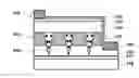
FIG. 1 is a diagrammatic cross section of the light-emitting diode according to Embodiment 1 of the present disclosure.
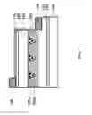
FIG. 2 is a diagrammatic cross section of the light-emitting diode according to Embodiment 2 of the present disclosure.
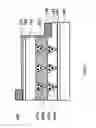
FIG. 3 is a diagrammatic cross section of the light-emitting diode according to Embodiment 3 of the present disclosure.
In the drawings:
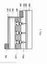
100: substrate; 101: buffer layer; 102: N-type layer; 103: MQW light-emitting layer; 104: P-type layer; 105: transparent conducting layer; 106a/106b/106c: V pit; 107a/107b/107c: metal nanoparticles; 108: N electrode; 109: P electrode; 110: insulating protective layer.
DETAILED DESCRIPTION
The light-emitting diode in the preferable embodiment of the present disclosure will be described in detail below with reference to the drawings.
Embodiment 1
As shown in FIG. 1, a light-emitting diode, comprising, from bottom to up:
(1) a substrate 100, like sapphire (Al2O3), SiC, Si or GaN. This embodiment preferably adopts sapphire substrate;
(2) a buffer layer 101 over the substrate 100 after high temperature treatment; the buffer layer is a 5-50 nm thick gallium nitride (GaN) and/or an aluminum nitride (AlN) layer grown under 400-600° C.;
(3) a 10-10000 nm thick N-type layer 102 (in this embodiment, preferably, N-type GaN layer) over the buffer layer 101 grown at 0.1-10 μm/h rate under 800-1200° C. and 100-700 torr; and the doping source is preferably SiH4 with doping concentration of 1×10¹⁸−1×1021 cm−3;
(4) a MQW light-emitting layer 103 over the N-type layer 102; the MQW light-emitting layer 103 is laminated by (InxGa1-xN/GaN)n periodic well layer/cladding layer at 0.01-1 μm/h under 600-900° C. and 100-700 torr, in which, the periodic number n is 2 - 2-100 and preferably 5-10; the InxGa1-xN well layer is about 1-100 nm thick, and In component 0<x<1; and the GaN cladding layer is about 5-100 nm thick, which is non-doping or N-type doping, wherein, N-type doping concentration is 1×10¹⁶−1×1020 cm−3 and the doping source is preferably SiH4. A V pit 106a is formed by adjusting growth rate, thickness, temperature, pressure or doping of the MQW light-emitting layer 103 well layer/cladding layer. The V pit 106a in the MQW light-emitting layer 103 is about 10-1000 nm and the density is about 1×10⁷−1×10¹⁰/cm2. At least one kind of metal nanoparticles 107a is filled in the V pit 106a, wherein, the metal nanoparticle 107a is at least one of main group metal or metalloid with particle diameter of 1-100 nm and thickness of 1-500 nm;
(5) a 50-300 nm P-type layer 104 (in this embodiment, preferably, P-type GaN layer) over the MQW light-emitting layer 103 grown under 900-1000° C.; and the doping source is preferably CP2Mg with doping concentration of 1×10¹⁹−1×1021 cm−3;
(6) a transparent conducting layer 105, either transparent conducting oxide layer or nitride layer, over the P-type layer 104; and this embodiment preferably adopts indium tin oxide (ITO);
(7) an N electrode 108 over the partially-exposed N-type layer 102 through etching;
(8) a P electrode 109 over the transparent conducting layer 105; and
(9) an insulating protective layer 110 over the light-emitting diode surface for protecting the light-emitting diode.
Embodiment 2
As shown in FIG. 2, a light-emitting diode is provided. Different from Embodiment 1, further, in step (3), the N-type layer 102 forms a V pit during epitaxial process and the V pit at least is filled in with a kind of metal nanoparticles. A V pit 106b is formed in the N-type layer by adjusting growth rate, thickness, temperature, pressure or doping of the N-type layer 102. The V pit 106b in the N-type layer is about 10-1000 nm and the density is about 1×10⁷−1×10¹⁰/cm2. At least one kind of metal nanoparticles 107b is filled in the V pit 106b, wherein, the metal nanoparticle 107b is at least one of main group metal or metalloid with particle diameter of 1-100 nm and thickness of 1-500 nm.
Embodiment 3
As shown in FIG. 3, a light-emitting diode is provided. Different from Embodiment 2, in steps (3) and (4), a V pit 106c is formed throughout the N-type layer 102 and MQW light-emitting layer 103 by adjusting growth rate, thickness, temperature, pressure or doping of the N-type layer 102 and the MQW light-emitting layer 103. The V pit 106c is about 10-1000 nm and the density is about 1×10⁷−1×10¹⁰/cm2. At least one kind of metal nanoparticles 107c is filled in the V pit 106c, wherein, the metal nanoparticle 107c is at least one of main group metal or metalloid with particle diameter of 1-100 nm and thickness of 1-500 nm.
In the light-emitting diode fabricated as above, surface plasma coupling effect is generated by filling metal nanoparticles in the V pit of the MQW light-emitting layer to inhibit coupling of electrons or holes with phonons and improve recombination probability of holes and electrons, thus improving internal quantum efficiency; and higher coupling efficiency and internal quantum efficiency are achieved in comparison to filling metal nanoparticles in the P-type layer. Further, surface plasma coupling effect is generated by filling metal nanoparticles in the V pit of the N-type layer to increase light reflection, light extraction efficiency and external quantum efficiency, thereby improving light emitting efficiency of the light-emitting diode. And the V pit is formed during epitaxial process directly by adjusting growth rate, thickness, temperature, pressure or doping during epitaxial process instead of etching, which causes no damage to the LED epitaxial layer, thus simplifying process and improving device stability.
All references referred to in the present disclosure are incorporated by reference in their entirety. Although specific embodiments have been described above in detail, the description is merely for purposes of illustration. It should be appreciated, therefore, that many aspects described above are not intended as required or essential elements unless explicitly stated otherwise. Various modifications of, and equivalent acts corresponding to, the disclosed aspects of the exemplary embodiments, in addition to those described above, can be made by a person of ordinary skill in the art, having the benefit of the present disclosure, without departing from the spirit and scope of the disclosure defined in the following claims, the scope of which is to be accorded the broadest interpretation so as to encompass such modifications and equivalent structures.
Claims
1. A light-emitting diode, comprising an N-type layer, a light-emitting layer, and a P-type layer, wherein at least one of the light-emitting layer or the N-type layer has one or more “V”-shaped indentations formed therein, and wherein the one or more “V”-shaped indentations have at least one type of metal nanoparticles disposed therein.
2. The light-emitting diode of claim 1, wherein the one or more “V”-shaped indentations are formed in the N-type layer.
3. The light-emitting diode of claim 1, wherein the one or more “V”-shaped indentations are formed through an epitaxial process.
4. The light-emitting diode of claim 3, wherein the one or more “V”-shaped indentations are formed by adjusting at least one of a growth rate, a thickness, a temperature, a pressure, or a doping during the epitaxial process.
5. The light-emitting diode of claim 1, wherein the one or more “V”-shaped indentations have a size of about 10-1000 nm.
6. The light-emitting diode of claim 1, wherein a density of the one or more “V”-shaped indentation is about 1×10⁷−1×10¹⁰/cm2.
7. The light-emitting diode of claim 1, wherein the metal nanoparticles comprise at least one of a main-group metal or a metalloid, and wherein the light-emitting layer has one or more “V”-shaped indentations disposed therein.
8. The light-emitting diode of claim 7, wherein a diameter of the metal nanoparticles is about 1-100 nm, and wherein both the light-emitting layer and the N-layer have one or more “V”-shaped indentations disposed therein.
9. The light-emitting diode of claim 7, wherein a thickness of the metal nanoparticles is about 1-500 nm, and wherein the light-emitting layer and the N-layer have one or more “V”-shaped indentations disposed therethrough.
10. The light-emitting diode of claim 1, wherein the N-type layer comprises at least one of an N-type GaN layer, an N-type AlN layer, an N-type InN layer, an N-type AlGaN layer, an N-type InGaN layer, or an N-type AlInGaN layer; and wherein the P-type layer comprises at least one of a P-type GaN layer, a P-type AlN layer, a P-type InN layer, a P-type AlGaN layer, a P-type InGaN layer, or a P-type AlInGaN layer.
11. A light-emitting system comprising a plurality of light-emitting diodes (LED), each LED comprising an N-type layer, a light-emitting layer, and a P-type layer, wherein at least one of the light-emitting layer or the N-type layer has one or more “V”-shaped indentations formed therein, and wherein the one or more “V”-shaped indentations have at least one type of metal nanoparticles disposed therein.
12. The system of claim 11, wherein the one or more “V”-shaped indentations are formed in the N-type layer.
13. The system of claim 11, wherein the one or more “V”-shaped indentations are formed through an epitaxial process.
14. The system of claim 11, wherein the one or more “V”-shaped indentations are formed by adjusting at least one of a growth rate, a thickness, a temperature, a pressure, or a doping during the epitaxial process.
15. The system of claim 11, wherein the one or more “V”-shaped indentations have a size of about 10-1000 nm.
16. The system of claim 11, wherein a density of the one or more “V”-shaped indentations is about 1×10⁷−1×10/cm2.
17. The system of claim 11, wherein the metal nanoparticles comprise at least one of a main-group metal or a metalloid, and wherein the light-emitting layer has one or more “V”-shaped indentations disposed therein.
18. The system of claim 17, wherein a diameter of the metal nanoparticles is about 1-100 nm, and wherein both the light-emitting layer and the N-layer have one or more “V”-shaped indentations disposed therein.
19. The system of claim 17, wherein a thickness of the metal nanoparticles is about 1-500 nm, and wherein the light-emitting layer and the N-layer have one or more “V”-shaped indentations disposed therethrough.
20. The system of claim 11, wherein the N-type layer comprises at least one of an N-type GaN layer, an N-type AlN layer, an N-type InN layer, an N-type AlGaN layer, an N-type InGaN layer, or an N-type AlInGaN layer; and wherein the P-type layer comprises at least one of a P-type GaN layer, a P-type AlN layer, a P-type InN layer, a P-type AlGaN layer, a P-type InGaN layer, or a P-type AlInGaN layer.
Images & Drawings included:
Sources:
- United States Patent and Trademark Office - verify current appl. status at the USPTO↗
Similar patent applications:
- » 20080121903
METHOD FOR MANUFACTURING LIGHT-EMITTING DIODE, LIGHT-EMITTING DIODE, LIGHTSOURCE CELL UNIT, LIGHT-EMITTING DIODE BACKLIGHT, LIGHT-EMITTING DIODE ILLUMINATING DEVICE, LIGHT-EMITTING DIODE DISPLAY, AND ELECTRONIC APPARATUS - » 20100308349
LIGHT-EMITTING DIODE, METHOD FOR MAKING LIGHT-EMITTING DIODE, INTEGRATED LIGHT-EMITTING DIODE AND METHOD FOR MAKING INTEGRATED LIGHT-EMITTING DIODE, METHOD FOR GROWING A NITRIDE-BASED III-V GROUP COMPOUND SEMICONDUCTOR, LIGHT SOURCE CELL UNIT, LIGHT-EMITTING DIODE BACKLIGHT, AND LIGHT-EMITTING DIODE DISPLAY AND ELECTRONIC DEVICE - » 20060258027
Light-emitting diode, method for making light-emitting diode, integrated light-emitting diode and method for making integrated light-emitting diode, method for growing a nitride-based III-V group compound semiconductor, light source cell unit, light-emitting diode - » 20140327028
Light-emitting diode, method for manufacturing light-emitting diode, light-emitting diode lamp and illumination device - » 20120199873
METAL SUBSTRATE FOR LIGHT-EMITTING DIODE, LIGHT-EMITTING DIODE, AND METHOD FOR MANUFACTURING LIGHT-EMITTING DIODE - » 20110298002
LIGHT-EMITTING DIODE, LIGHT-EMITTING DIODE LAMP, METHOD FOR MANUFACTURING LIGHT-EMITTING DIODE - » 20080283853
Light-emitting diode, light-emitting diode substrate and production method of light-emitting diode - » 20240047618
LIGHT-EMITTING DIODE, LIGHT-EMITTING DIODE PACKAGE, AND LIGHT-EMITTING DEVICE - » 20210119086
Light-emitting diode, and light-emitting diode package, light-emitting diode module and display device including the same - » 20250029934
LIGHT-EMITTING DIODE, LIGHT-EMITTING DIODE CHIPLET AND LIGHT-EMITTING DEVICE
Recent applications in this class:
- » 20250063859 2025-02-20
ALUMINUM NITRIDE SINGLE CRYSTAL SUBSTRATE, SEMICONDUCTOR WAFER USING THE ALUMINUM NITRIDE SINGLE CRYSTAL SUBSTRATE, AND MANUFACTURING METHODS OF THE SAME - » 20250040305 2025-01-30
METHOD FOR MANUFACTURING SEPARABLE SEMICONDUCTOR SUBSTRATE, AND SEMICONDUCTOR SUBSTRATE, THIN FILM DEVICE AND COMPOSITE DEVICE MANUFACTURED BY THE SAME - » 20250040304 2025-01-30
NITRIDE SEMICONDUCTOR LIGHT-EMITTING ELEMENT - » 20250040303 2025-01-30
LIGHT EMITTING ELEMENT AND DISPLAY DEVICE USING LIGHT EMITTING ELEMENT - » 20250040302 2025-01-30
ULTRAVIOLET LIGHT-EMITTING ELEMENT AND METHOD OF PRODUCING SAME - » 20250031491 2025-01-23
LIGHT-EMITTING DEVICE AND METHOD OF MANUFACTURING THE SAME - » 20250015231 2025-01-09
A LIGHT EMITTING DIODE EPITAXIAL STRUCTURE BASED ON ALUMINUM GALLIUM NITRIDE MATERIAL AND ITS MANUFACTURING METHOD - » 20240429347 2024-12-26
RGB FULL-COLOR InGaN-BASED LED AND METHOD FOR PREPARING THE SAME - » 20240421255 2024-12-19
METHOD FOR PROCESSING AN OPTOELECTRONIC COMPONENT AND OPTOELECTRONIC COMPONENT - » 20240379907 2024-11-14
GROUP III ELEMENT NITRIDE SEMICONDUCTOR SUBSTRATE AND BONDED SUBSTRATE
Recent applications for this Assignee:
- » 20250169242 2025-05-22
INFRARED LIGHT-EMITTING DIODE, INFRARED LIGHT-EMITTING DIODE PACKAGE, AND LIGHT-EMITTING DEVICE - » 20250081682 2025-03-06
LIGHT-EMITTING DEVICE AND MANUFACTURING METHOD THEREOF AND DISPLAY SCREEN - » 20250081677 2025-03-06
FLIP-CHIP LIGHT-EMITTING ELEMENT AND LIGHT-EMITTING DEVICE - » 20250056929 2025-02-13
LIGHT EMITTING DIODE, LIGHT EMITTING DEVICE, AND MANUFACTURING METHOD FOR LIGHT EMITTING DIODE - » 20250048791 2025-02-06
LIGHT EMITTING DIODE AND LIGHT EMITTING DEVICE - » 20250040308 2025-01-30
LIGHT EMITTING DIODE AND LIGHT EMITTING DEVICE - » 20250015230 2025-01-09
LIGHT EMITTING DIODE - » 20240339569 2024-10-10
LIGHT EMITTING DIODE AND LIGHT EMITTING DEVICE - » 20240290912 2024-08-29
LIGHT EMITTING DIODE AND LIGHT EMITTING DEVICE - » 20240222563 2024-07-04
LIGHT-EMITTING ELEMENT AND LIGHT-EMITTING DEVICE