Flip-chip mounted semiconductor device
US20160126155A1
2016-05-05
14/927,040
2015-10-29
✅ Patent granted
US 9,704,771 B2
2017-07-11
-
-
Julio J Maldonado | Moin Rahman
Adams & Wilks
2035-10-29
Abstract:
Provided is a flip-chip mounted semiconductor device in which a crack is less likely to develop. Flip chip mounting is carried out under the condition that no oxide film exists on the scribe region so as to eliminate the interface between the oxide film that remains on the scribe region and the silicon substrate from which a crack may develop. As a result, the circuit board, the encapsulant, and the silicon substrate are stacked at an end portion of the semiconductor chip.
Inventors:
- Kotaro WATANABE 24 🇯🇵 Chiba, Japan
- Kotaro WATANABE 25 🇯🇵 Chiba-shi, Japan
- Yukimasa MINAMI 16 🇯🇵 Chiba, Japan
- Yukimasa MINAMI 14 🇯🇵 Chiba-shi, Japan
- Yoichi MIMURO 5 🇯🇵 Chiba-shi, Japan
- Yoichi Mimuro 5 🇯🇵 Chiba, Japan
Assignee:
- SII Semiconductor Corporation 70 🇯🇵 , Japan
Applicant:
Interested in similar patents?
Get notified when new applications in this technology area are published.
Classification:
H01L23/49816 » CPC further
Details of semiconductor or other solid state devices; Arrangements for conducting electric current to or from the solid state body in operation, e.g. leads, terminal arrangements ; Selection of materials therefor consisting of soldered constructions; Leads, on insulating substrates,; Additional leads joined to the metallisation on the insulating substrate, e.g. pins, bumps, wires, flat leads Spherical bumps on the substrate for external connection, e.g. ball grid arrays [BGA]
H01L23/564 » CPC further
Details of semiconductor or other solid state devices Details not otherwise provided for, e.g. protection against moisture
H01L23/498 IPC
Details of semiconductor or other solid state devices; Arrangements for conducting electric current to or from the solid state body in operation, e.g. leads, terminal arrangements ; Selection of materials therefor consisting of soldered constructions Leads, on insulating substrates,
H01L23/3178 » CPC main
Details of semiconductor or other solid state devices; Encapsulations, e.g. encapsulating layers, coatings, e.g. for protection characterised by the arrangement or shape; Partial encapsulation or coating Coating or filling in grooves made in the semiconductor body
H01L23/562 » CPC further
Details of semiconductor or other solid state devices Protection against mechanical damage
H01L23/31 IPC
Details of semiconductor or other solid state devices; Encapsulations, e.g. encapsulating layers, coatings, e.g. for protection characterised by the arrangement or shape
H01L23/00 IPC
Details of semiconductor or other solid state devices
H01L21/563 » CPC further
Processes or apparatus adapted for the manufacture or treatment of semiconductor or solid state devices or of parts thereof; Manufacture or treatment of semiconductor devices or of parts thereof the devices having at least one potential-jump barrier or surface barrier, e.g. PN junction, depletion layer or carrier concentration layer; Assembly of semiconductor devices using processes or apparatus not provided for in a single one of the subgroups - , e.g. sealing of a cap to a base of a container; Encapsulations, e.g. encapsulation layers, coatings Encapsulation of active face of flip-chip device, e.g. underfilling or underencapsulation of flip-chip, encapsulation preform on chip or mounting substrate
H01L29/0657 » CPC further
Semiconductor devices adapted for rectifying, amplifying, oscillating or switching, or capacitors or resistors with at least one potential-jump barrier or surface barrier, e.g. PN junction depletion layer or carrier concentration layer; Details of semiconductor bodies or of electrodes thereof; Multistep manufacturing processes therefor; Semiconductor bodies ; Multistep manufacturing processes therefor characterised by their shape; characterised by the shapes, relative sizes, or dispositions of the semiconductor regions ; characterised by the concentration or distribution of impurities within semiconductor regions characterised by the shape of the body
H01L2224/73204 » CPC further
Indexing scheme for arrangements for connecting or disconnecting semiconductor or solid-state bodies and methods related thereto as covered by; Means for bonding being of different types provided for in two or more of groups; Location after the connecting process on the same surface; Bump and layer connectors the bump connector being embedded into the layer connector
H01L2224/92125 » CPC further
Indexing scheme for arrangements for connecting or disconnecting semiconductor or solid-state bodies and methods related thereto as covered by; Methods for connecting semiconductor or solid state bodies including different methods provided for in two or more of groups - ; Specific sequence of method steps; Connecting a surface with connectors of different types; Sequential connecting processes the first connecting process involving a bump connector the second connecting process involving a layer connector
H01L23/48 IPC
Details of semiconductor or other solid state devices Arrangements for conducting electric current to or from the solid state body in operation, e.g. leads, terminal arrangements ; Selection of materials therefor
H01L21/56 IPC
Processes or apparatus adapted for the manufacture or treatment of semiconductor or solid state devices or of parts thereof; Manufacture or treatment of semiconductor devices or of parts thereof the devices having at least one potential-jump barrier or surface barrier, e.g. PN junction, depletion layer or carrier concentration layer; Assembly of semiconductor devices using processes or apparatus not provided for in a single one of the subgroups - , e.g. sealing of a cap to a base of a container Encapsulations, e.g. encapsulation layers, coatings
H01L29/06 IPC
Semiconductor devices adapted for rectifying, amplifying, oscillating or switching, or capacitors or resistors with at least one potential-jump barrier or surface barrier, e.g. PN junction depletion layer or carrier concentration layer; Details of semiconductor bodies or of electrodes thereof; Multistep manufacturing processes therefor; Semiconductor bodies ; Multistep manufacturing processes therefor characterised by their shape; characterised by the shapes, relative sizes, or dispositions of the semiconductor regions ; characterised by the concentration or distribution of impurities within semiconductor regions
Description
BACKGROUND OF THE INVENTION
1. Field of the Invention
The present invention relates to a semiconductor device in which a semiconductor chip is flip-chip mounted on a circuit board.
2. Description of the Related Art
In manufacturing a semiconductor device, there is employed a flip chip mounting technology in which a semiconductor chip is mounted on a circuit board via a bump with an element surface thereof confronting the circuit board. In the flip chip mounting, connection between the circuit board and the semiconductor chip is made by forming a solder bump or the like on the semiconductor chip side, and then pressing the solder bump or the like against wiring formed on the circuit board. An encapsulant such as an epoxy resin is filled between the circuit board and the semiconductor chip for the purpose of securing moisture resistance or alleviating stress on the solder bump from the circuit board.
The encapsulant described above has a thermal expansion coefficient that is higher than that of the semiconductor chip, and thus, during an environmental test such as a temperature cycling test, large thermal stress is applied on the semiconductor chip. The semiconductor chip and the circuit board also have different thermal expansion coefficients, and thus, large stress is applied to the encapsulant as well. As a result, in the temperature cycling test, due to such stress, the solder bump connection will become unstable and a crack will develop in the semiconductor chip.
It is described in Japanese Patent Application Laid-open No. 2002-170848 that, in order to avoid such problems, a bump only for joining is formed in a center region of each side of the semiconductor chip where no bump is hitherto formed and is connected to the circuit board, to thereby improve reliability.
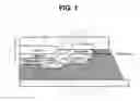
Further, in the filling step of the encapsulant, when an amount and an injection direction of the encapsulant are efficient, the encapsulant does not cover a side surface of the chip in the formed structure, which is illustrated in FIG. 2. A semiconductor chip 10 is faced down and connected to a circuit board 7 via a bump (not shown). An encapsulant 6 is filled between the semiconductor chip 10 and the circuit board 7. Such a structure is also disclosed in Japanese Patent Application Laid-open No. 2002-170848.
When an encapsulant has such a shape, an end portion of the encapsulant is in contact with a scribe region defined by the double-headed arrow in an outer peripheral portion of the semiconductor chip 10. Stress concentrates in a vicinity of the end portion of the encapsulant, and large thermal stress is applied to the scribe region of the semiconductor chip 10. A crack may then develop from an interface between an oxide film (interlayer insulating film) 3 that remains on the scribe region of the semiconductor chip 10 and a silicon substrate 1 to reach an inside of the semiconductor chip 10. Once a crack develops, the crack breaks a junction portion formed in the semiconductor chip 10, and thus, leakage current is produced, which may increase current consumption or may result in a circuit malfunction.
SUMMARY OF THE INVENTION
Accordingly, an object of the present invention is to provide a semiconductor device using a semiconductor chip suitable for flip chip mounting having a scribe region structure, which can bear a temperature cycling test to a sufficient extent.
In order to solve the problem described above, according to one embodiment of the present invention, there is provided a structure in which no oxide film exists on a scribe region so as to eliminate an interface between an oxide film that remains on a scribe region and a silicon substrate from which a crack may develop, and flip chip mounting is carried out while keeping the structure. As a result, a circuit board, an encapsulant, and the silicon substrate are stacked in an outer peripheral portion of a semiconductor chip, and thus, large stress is prevented from being applied between an oxide film serving as an interlayer film and the silicon substrate.
According to the one embodiment of the present invention, even in an environment state in which thermal stress is applied, no crack develops in the flip-chip mounted semiconductor chip. Therefore, reliability is improved and effects of stabled characteristics and prevention of deterioration over time may be obtained.
BRIEF DESCRIPTION OF THE DRAWINGS
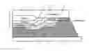
FIG. 1 is a sectional view for illustrating a semiconductor device according to an embodiment of the present invention in which a semiconductor chip is flip-chip mounted on a circuit board.
FIG. 2 is a sectional view for illustrating a related-art semiconductor device in which a semiconductor chip is flip-chip mounted on a circuit board.
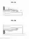
FIGS. 3A-3C are sectional views for illustrating manufacturing steps of the semiconductor device according to the embodiment of the present invention.
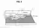
FIG. 4 is a sectional view for illustrating a semiconductor device according to another embodiment of the present invention.
DETAILED DESCRIPTION OF THE EMBODIMENTS
FIG. 1 is a sectional view for illustrating a semiconductor device according to an embodiment of the present invention in which a semiconductor chip is flip-chip mounted on a circuit board. In the semiconductor device in which the semiconductor chip is flip-chip mounted on the circuit board with an element surface thereof confronting the circuit board, a semiconductor chip 10 is faced down and connected to a circuit board 7 via a bump (not shown). An encapsulant 6 is filled between the semiconductor chip 10 and the circuit board 7. In this case, an end portion of the encapsulant 6 is in contact with a scribe region defined by the double-headed arrow in an outer peripheral portion of the semiconductor chip 10. The semiconductor chip 10 includes a field oxide film 2 formed on a surface of a silicon substrate 1, an interlayer insulating film 3 formed so as to extend from the field oxide film 2 to the surface of the silicon substrate 1, a metal wiring layer 4 formed on the interlayer insulating film 3, and a protective film 5 formed on the metal wiring layer 4.
An important point in FIG. 1 is absence of the interlayer insulating film 3 on the scribe region. In this embodiment, together with an end surface of the protective film 5, an end surface of the interlayer insulating film 3 is exposed only at an interface with the scribe region.
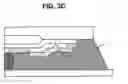
FIG. 3A to FIG. 3C are sectional views for illustrating manufacturing steps of the semiconductor device according to the embodiment of the present invention, which schematically illustrate steps for manufacturing the semiconductor device according to the embodiment illustrated in FIG. 1 in order of steps. First, as illustrated in FIG. 3A, the semiconductor chip 10 is manufactured using a semiconductor process suitable for a function thereof. A typical structure of the semiconductor chip 10 includes, similarly to that illustrated in FIG. 1, the silicon substrate 1, the field oxide film 2 formed on the surface of the silicon substrate 1, the interlayer insulating film 3 formed so as to extend from the field oxide film 2 to the surface of the silicon substrate 1, the metal wiring layer 4 formed on the interlayer insulating film 3, the protective film 5 formed on the metal wiring layer 4, and a solder bump 8 formed on a so-called pad portion that is an exposed portion of metal wiring having no protective film 5 formed thereon.
Various kinds of metal films stacked in steps of the semiconductor process for manufacturing such a structure are etched out on the scribe region. Only a portion of the insulating film 3 on the scribe region is etched out after a step of patterning the protective film 5 is completed. Alternatively, etching out may be carried out in steps of patterning various kinds of insulating films. The semiconductor chip 10 after the insulating film 3 on the scribe region is removed in this way is turned upside down and is mounted on the circuit board 7.
When, for example, as illustrated in FIG. 3B, the solder bump 8 is formed on the semiconductor chip 10 and is suitable for flip chip mounting, the solder bump 8 is connected to a track of the circuit board 7. For the purpose of melting solder for adhesion, heat treatment for a short time is carried out, and the solder bump 8 on the semiconductor chip 10 is pressed against the track on the circuit board 7.
After that, as illustrated in FIG. 3C, for the purpose of improving environmental resistance and moisture resistance, the encapsulant 6 is injected between the semiconductor chip 10 and the circuit board 7, and curing treatment thereof is appropriately applied. In a step of filling the encapsulant 6, when an amount and an injection direction of the encapsulant 6 are efficient, the encapsulant 6 does not cover a side surface of the chip 10 in the formed structure as illustrated in FIG. 3C. Specifically, the encapsulant 6 is only in contact with a front surface of the semiconductor chip 10, and is not in contact with the side surface of the semiconductor chip 10.
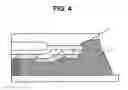
FIG. 4 is a sectional view for illustrating a semiconductor device according to another embodiment of the present invention. When various kinds of insulating films are etched out in steps of patterning the insulating films, by removing a last insulating film using isotropic etching with carbon fluoride, the silicon substrate 1 in the scribe region is isotropically etched as illustrated in FIG. 4. The silicon substrate 1 becomes thinner from the inside toward a periphery thereof. In such a shape, similarly to the case of the embodiment described above, the interlayer insulating film 3 does not exist on the scribe region, and the encapsulant 6 is indirect contact with the semiconductor chip 10, and thus, a crack does not develop in the semiconductor chip 10. Further, the silicon substrate 1 has a depression 9 formed by the etching. The encapsulant 6 is filled in the depression 9, and, as a result, the depression 9 is in a shape of gripping the encapsulant 6, and thus, adherence between the silicon substrate 1 and the encapsulant 6 can be enhanced.
Claims
What is claimed is:1. A flip-chip mounted semiconductor device, comprising:
a circuit board;
a semiconductor chip comprising a silicon substrate, and connected to the circuit board with an element surface of the semiconductor chip confronting the circuit board; and
an encapsulant filling a space between the semiconductor chip and the circuit board,
the encapsulant not covering a side surface of the semiconductor chip, and the side surface being exposed.
2. A semiconductor device according to claim 1, wherein silicon of the silicon substrate is exposed from a region of a scribe region of the semiconductor chip, and the encapsulant and the silicon substrate are in direct contact with each other at the region.
3. A semiconductor device according to claim 2, wherein the silicon is exposed in a depressed region and the encapsulant fills the depressed region.
Images & Drawings included:
Sources:
- United States Patent and Trademark Office - verify current appl. status at the USPTO↗
Similar patent applications:
- » 20090159902
Flip-chip type semiconductor light-emitting device, method for manufacturing flip-chip type semiconductor light-emitting device, printed circuit board for flip-chip type semiconductor light-emitting device, mounting structure for flip-chip type semiconductor light-emitting device, and light-emitting diode lamp - » 20110175237
Semiconductor device, flip-chip mounting method and flip-chip mounting apparatus - » 20100105173
METHOD OF PRODUCING SEMICONDUCTOR DEVICE PROVIDED WITH FLIP-CHIP MOUNTED SEMICONDUCTOR ELEMENT - » 20120326301
THERMOSETTING RESIN COMPOSITION, FLIP-CHIP MOUNTING ADHESIVE, SEMICONDUCTOR DEVICE FABRICATION METHOD, AND SEMICONDUCTOR DEVICE - » 20170081175
Electronic sensor device including a flip-chip mounted semiconductor chip and a substrate with an opening - » 10177672
Semiconductor device including semiconductor bare chip mounted by flip-chip bonding, and board member with thin-film structure capacitor for semiconductor bare chip mounted by flip-chip bonding - » 20080224325
Wiring board for flip-chip mounting, mounting structure of electronic components on wiring board, and semiconductor device including wiring board
Recent applications in this class:
- » 20250246495 2025-07-31
Chip - » 20250246494 2025-07-31
SEMICONDUCTOR STRUCTURE AND MANUFACTURING METHOD THEREOF - » 20250118612 2025-04-10
SEMICONDUCTOR PACKAGE AND METHOD OF FABRICATING THE SAME - » 20250096059 2025-03-20
Integrated Fan Out Device with a Filler-Free Insulating Material - » 20240421020 2024-12-19
SEMICONDUCTOR PACKAGE - » 20240371717 2024-11-07
SEMICONDUCTOR DEVICE - » 20240297089 2024-09-05
PACKAGE STRUCTURE AND METHOD FOR FORMING THE SAME - » 20240290678 2024-08-29
SEMICONDUCTOR STRUCTURE AND METHOD FOR PREPARING SAME, MEMORY, AND ELECTRONIC DEVICE - » 20240274486 2024-08-15
ELECTRONIC DEVICE AND MANUFACTURING METHOD THEREOF - » 20240213109 2024-06-27
SEMICONDUCTOR PACKAGE WITH SEMICONDUCTOR DEVICES
Recent applications for this Assignee:
- » 20170351180 2017-12-07
Reticle transmittance measurement method, projection exposure method using the same, and projection exposure device - » 20170263521 2017-09-14
Resin-encapsulated semiconductor device - » 20170257028 2017-09-07
Switching regulator for detecting a plurality of abnormalities using only one comparison circuit - » 20170256582 2017-09-07
Semiconductor device and a method of manufacturing a semiconductor device - » 20170256545 2017-09-07
Method of manufacturing semiconductor integrated circuit device - » 20170162588 2017-06-08
Semiconductor nonvolatile memory element - » 20170025320 2017-01-26
Resin-encapsulatd semiconductor device and method of manufacturing the same - » 20170005174 2017-01-05
Method of manufacturing a semiconductor device - » 20160351731 2016-12-01
Optical sensor device - » 20160351730 2016-12-01
Optical sensor device