Metal-oxide-semiconductor field-effect transistor with metal-insulator-semiconductor contact structure to reduce schottky barrier
US20160133714A1
2016-05-12
14/981,489
2015-12-28
✅ Patent granted
US 9,536,973 B2
2017-01-03
-
-
Benjamin Sandvik
Slater Matsil, LLP
2035-12-28
Abstract:
A method includes depositing a first metal layer on a native SiO2 layer that is disposed on at least one of a source and a drain of a metal-oxide-semiconductor field-effect transistor (MOSFET). A metal oxide layer is formed from the native SiO2 layer and the first metal layer, wherein the remaining first metal layer, the metal oxide layer, and the at least one of the source and the drain form a metal-insulator-semiconductor (MIS) contact.
Assignee:
- TAIWAN SEMICONDUCTOR MANUFACTURING COMPANY, LTD. 8,890 🇹🇼 Hsin-Chu, Taiwan
Applicant:
Interested in similar patents?
Get notified when new applications in this technology area are published.
Classification:
H01L2924/0002 » CPC further
Indexing scheme for arrangements or methods for connecting or disconnecting semiconductor or solid-state bodies as covered by; Technical content checked by a classifier Not covered by any one of groups , and
H01L29/41725 » CPC further
Semiconductor devices adapted for rectifying, amplifying, oscillating or switching, or capacitors or resistors with at least one potential-jump barrier or surface barrier, e.g. PN junction depletion layer or carrier concentration layer; Details of semiconductor bodies or of electrodes thereof; Multistep manufacturing processes therefor; Electrodes ; Multistep manufacturing processes therefor characterised by their shape, relative sizes or dispositions carrying the current to be rectified, amplified or switched Source or drain electrodes for field effect devices
H01L21/76831 » CPC further
Processes or apparatus adapted for the manufacture or treatment of semiconductor or solid state devices or of parts thereof; Manufacture or treatment of devices consisting of a plurality of solid state components formed in or on a common substrate or of parts thereof; Manufacture of integrated circuit devices or of parts thereof; Manufacture of specific parts of devices defined in group; Applying interconnections to be used for carrying current between separate components within a device comprising conductors and dielectrics characterised by the formation and the after-treatment of the dielectrics, e.g. smoothing characterised by the formation of thin functional dielectric layers, e.g. dielectric etch-stop, barrier, capping or liner layers in via holes or trenches, e.g. non-conductive sidewall liners
H01L21/76843 » CPC further
Processes or apparatus adapted for the manufacture or treatment of semiconductor or solid state devices or of parts thereof; Manufacture or treatment of devices consisting of a plurality of solid state components formed in or on a common substrate or of parts thereof; Manufacture of integrated circuit devices or of parts thereof; Manufacture of specific parts of devices defined in group; Applying interconnections to be used for carrying current between separate components within a device comprising conductors and dielectrics characterised by the formation and the after-treatment of the conductors; Barrier, adhesion or liner layers formed in openings in a dielectric
H01L21/768 IPC
Processes or apparatus adapted for the manufacture or treatment of semiconductor or solid state devices or of parts thereof; Manufacture or treatment of devices consisting of a plurality of solid state components formed in or on a common substrate or of parts thereof; Manufacture of integrated circuit devices or of parts thereof; Manufacture of specific parts of devices defined in group Applying interconnections to be used for carrying current between separate components within a device comprising conductors and dielectrics
H01L29/458 » CPC further
Semiconductor devices adapted for rectifying, amplifying, oscillating or switching, or capacitors or resistors with at least one potential-jump barrier or surface barrier, e.g. PN junction depletion layer or carrier concentration layer; Details of semiconductor bodies or of electrodes thereof; Multistep manufacturing processes therefor; Electrodes ; Multistep manufacturing processes therefor characterised by the materials of which they are formed; Ohmic electrodes on silicon for thin film silicon, e.g. source or drain electrode
H01L23/485 » CPC further
Details of semiconductor or other solid state devices; Arrangements for conducting electric current to or from the solid state body in operation, e.g. leads, terminal arrangements ; Selection of materials therefor consisting of lead-in layers inseparably applied to the semiconductor body consisting of layered constructions comprising conductive layers and insulating layers, e.g. planar contacts
H01L29/45 » CPC main
Semiconductor devices adapted for rectifying, amplifying, oscillating or switching, or capacitors or resistors with at least one potential-jump barrier or surface barrier, e.g. PN junction depletion layer or carrier concentration layer; Details of semiconductor bodies or of electrodes thereof; Multistep manufacturing processes therefor; Electrodes ; Multistep manufacturing processes therefor characterised by the materials of which they are formed Ohmic electrodes
H01L29/417 IPC
Semiconductor devices adapted for rectifying, amplifying, oscillating or switching, or capacitors or resistors with at least one potential-jump barrier or surface barrier, e.g. PN junction depletion layer or carrier concentration layer; Details of semiconductor bodies or of electrodes thereof; Multistep manufacturing processes therefor; Electrodes ; Multistep manufacturing processes therefor characterised by their shape, relative sizes or dispositions carrying the current to be rectified, amplified or switched
H01L29/78 » CPC further
Semiconductor devices adapted for rectifying, amplifying, oscillating or switching, or capacitors or resistors with at least one potential-jump barrier or surface barrier, e.g. PN junction depletion layer or carrier concentration layer; Details of semiconductor bodies or of electrodes thereof; Multistep manufacturing processes therefor; Types of semiconductor device ; Multistep manufacturing processes therefor controllable by only the electric current supplied, or only the electric potential applied, to an electrode which does not carry the current to be rectified, amplified or switched; Unipolar devices, e.g. field effect transistors; Field effect transistors with field effect produced by an insulated gate
H01L29/7833 » CPC further
Semiconductor devices adapted for rectifying, amplifying, oscillating or switching, or capacitors or resistors with at least one potential-jump barrier or surface barrier, e.g. PN junction depletion layer or carrier concentration layer; Details of semiconductor bodies or of electrodes thereof; Multistep manufacturing processes therefor; Types of semiconductor device ; Multistep manufacturing processes therefor controllable by only the electric current supplied, or only the electric potential applied, to an electrode which does not carry the current to be rectified, amplified or switched; Unipolar devices, e.g. field effect transistors; Field effect transistors with field effect produced by an insulated gate with lightly doped drain or source extension, e.g. LDD MOSFET's; DDD MOSFET's
Description
This application is a divisional of U.S. patent application Ser. No. 13/902,551, filed on May 24, 2013, entitled “Metal-Oxide-Semiconductor Field-Effect Transistor with Metal-Insulator-Semiconductor Contact Structure to Reduce Schottky Barrier,” and claims priority to U.S. Provisional Application Ser. No. 61/785,018, filed on Mar. 14, 2013, entitled “Method and Apparatus for a Metal-Insulator-Semiconductor Structure,” which application is incorporated herein by reference.
TECHNICAL FIELD
The present disclosure relates generally to an integrated circuit and more particularly to a metal-oxide-semiconductor field-effect transistor (MOSFET) with a metal-insulator semiconductor (MIS) contact structure.
BACKGROUND
The source/drain contact resistance of a conventional MOSFET using silicide has limited the performance of the MOSFET due to high Schottky barrier height between the silicide and the source/drain. A MIS structure can be an alternative contact scheme to source/drain to replace silicide and further reduce contact resistance. However, formation of the insulator has challenging issues of precision control for various devices across the entire wafer.
BRIEF DESCRIPTION OF THE DRAWINGS
Reference is now made to the following descriptions taken in conjunction with the accompanying drawings, in which:
FIG. 1 is a schematic diagram of an exemplary metal-oxide-semiconductor field-effect transistor (MOSFET) with a metal-insulator semiconductor (MIS) contact structure for source/drain according to some embodiments;
FIGS. 2A-2D are intermediate fabrication steps of the exemplary MOSFET with the MIS contact structure for source/drain in FIG. 1; and
FIG. 3 is a schematic diagram of another exemplary MOSFET with the MIS contact structure for source/drain according to some embodiments.
DETAILED DESCRIPTION
The making and using of various embodiments are discussed in detail below. It should be appreciated, however, that the present disclosure provides many applicable inventive concepts that can be embodied in a wide variety of specific contexts. The specific embodiments discussed are merely illustrative of specific ways to make and use, and do not limit the scope of the disclosure.
In addition, the present disclosure may repeat reference numerals and/or letters in the various examples. This repetition is for the purpose of simplicity and clarity and does not in itself dictate a relationship between the various embodiments and/or configurations discussed. Moreover, the formation of a feature on, connected to, and/or coupled to another feature in the present disclosure that follows may include embodiments in which the features are formed in direct contact, and may also include embodiments in which additional features may be formed interposing the features, such that the features may not be in direct contact. In addition, spatially relative terms, for example, “lower,” “upper,” “horizontal,” “vertical,” “above,” “over,” “below,” “beneath,” “up,” “down,” “top,” “bottom,” etc. as well as derivatives thereof (e.g., “horizontally,” “downwardly,” “upwardly,” etc.) are used for ease of the present disclosure of one features relationship to another feature. The spatially relative terms are intended to cover different orientations of the device including the features.
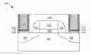
FIG. 1 is a schematic diagram of an exemplary metal-oxide-semiconductor field-effect transistor (MOSFET) 100 with a metal-insulator semiconductor (MIS) contact structure for source/drain according to some embodiments. The MOSFET 100 includes a substrate 102, source/drain 104, a gate dielectric layer 106, a gate electrode 108, spacers 110, a dielectric layer 112, a raised silicon layer 114 on the source/drain 104, a metal oxide layer 116, a first metal layer 118, and a second metal layer 120.
The substrate 102 comprises silicon or any other suitable material. The source/drain 104 formed in the substrate 102 is doped with N-type or P-type dopants such as phosphorous or boron. The gate dielectric layer 106 comprises SiO2 or any other suitable dielectric material. The gate electrode comprises polysilicon, metal, or any other suitable material. The spacers 110 comprise Si3N4, SiO2, or any other suitable material. The dielectric layer 112 comprises SiO2 or any other suitable material.
The first metal layer 118 comprises Ti, Hf, Zr, Al, or any other suitable material that has a stronger affinity to oxygen than the substrate (e.g. silicon) and high-k dielectric properties when oxidized in some embodiments. The metal oxide layer 116 comprises oxidized metal corresponding to the first metal layer 118, such as TiO2, HfO2, ZrO2, Al2O3, etc. The second metal layer 120 comprises any suitable metal such as Al, Cu, W, etc.
The first metal layer 118 can be deposited by a chemical vapor deposition (CVD) process or a physical vapor deposition (PVD) process. The thickness of the first metal layer 118 ranges from 10 Å to 20 Å in some embodiments. With CVD metal deposition, the sidewall metal thickness is about the same as the bottom. With PVD metal deposition, the sidewall metal thickness will be thinner than the bottom.
The raised silicon layer 114 results from a thermal process of a native SiO2 layer on the surface of the source/drain 104 adjacent the first metal layer 118 in some embodiments. The thermal process forms the metal oxide layer 116 and the raised silicon layer 114 based on metal oxygen scavenge effect as described with respect to FIGS. 2A-2D. Because the native SiO2 layer on the source/drain 104 has generally uniform thickness from 8 Å to 10 Å, the thickness of the resulting metal oxide layer 116 (i.e., insulator in the MIS structure) can be controlled with atomic precision to lower the Schottky barrier height for resistance reduction of the source/drain 104 contact.
In some embodiments, the raised silicon layer 114 on source/drain 104 has a thickness from 3 Å to 5 Å, and the metal oxide layer 116 has a thickness from 8 Å to 10 Å at the bottom and from 10 Å to 15 Å at the side. The thickness control of the insulator layer in the MIS structure (i.e., the metal oxide layer 116 at the bottom) could be achieved within 1 Å to 2 Å, since the self-limiting native SiO2 layer thickness variation range is 1 Å to 2 Å.
A rapid thermal anneal (RTA) process having a peak temperature from 300° C. to 600° C. and a peak time duration from 1 sec to 2 sec can be used in some embodiments. In another example, a rapid thermal anneal (RTA) process with a peak temperature from 700° C. to 1100° C. and a peak time duration in the order of milliseconds can be used.
The metal layers 118 and 120, the metal oxide layer 116, and the source/drain 104 including the raised silicon layer 114 form the MIS contact structure for the source/drain 104 with strong dielectric dipoles to significantly lower the contact resistance through Schottky barrier height reduction. The source/drain contact resistivity of the MIS structure in FIG. 1 is in the order of 10−8 ohm-cm in some embodiments, compared to the source/drain contact resistivity in the order of 10−7 ohm-cm for some other structure.
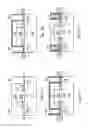
FIGS. 2A-2D are intermediate fabrication steps of the exemplary MOSFET 100 with the MIS contact structure for source/drain in FIG. 1. In FIG. 2A, a native SiO2 layer 202 is formed at the bottom of contact holes 204 on the source/drain 104. The native SiO2 layer 202 can be formed naturally under ambient conditions after etching the contact hole 204 and a cleaning process in some embodiments. The contact hole 204 is formed through the dielectric layer 112 disposed over the MOSFET towards the source/drain 104. The thickness of the native SiO2 layer 202 is typically from 8 Å to 10 Å. Since the thickness of the native SiO2 layer 202 is self-limiting on the source/drain 104, it can be uniformly controlled across the entire wafer.
In FIG. 2B, the first metal layer 118 is deposited on the native SiO2 layer 202 and over the source/drain 104 in the contact hole 204 using a chemical vapor deposition (CVD) process or a soft physical vapor deposition (PVD) process such as thermal evaporation without causing any metal and Si physical intermixing in some embodiments. The thickness of the first metal layer 118 ranges from 10 Å to 20 Å in some embodiments. With CVD metal deposition, the sidewall metal thickness is about the same as the bottom. With PVD metal deposition, the sidewall metal thickness will be thinner than the bottom.
The first metal layer 118 comprises Ti, Hf, Zr, Al, or any other suitable material that has a stronger affinity to oxygen than the substrate (e.g. silicon), and high-k dielectric properties when oxidized in some embodiments. For example, the first metal 118 can comprise Ti for NMOS or Al for PMOS for forming favorable dipoles to reduce the Schottky barrier height.
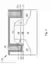
In FIG. 2C, a thermal process (e.g., annealing) is applied in a controlled ambient to trigger metal oxygen scavenge effect and to reduce the native SiO2 layer 202 to the raised silicon layer 114 and form the metal oxide layer 116 such as TiO2, HfO2, ZrO2, Al2O3, etc. depending on the first metal layer 118. The thermal process also results in the raised silicon layer 114. Part of the first metal layer 118 will react with the native SiO2 layer 202, and the rest remains.
The remaining first metal layer 118, the metal oxide layer 116, and the source/drain 104 (including the raised silicon layer 114) form a MIS structure with strong dielectric dipoles to significantly lower the Schottky barrier height and also reduce the associated contact resistance of the source/drain 104.
In some embodiments, the raised silicon layer 114 on the source/drain 104 has a thickness from 3 Å to 5 Å, and the metal oxide layer 116 has a thickness from 8 Å to 10 Å at the bottom and from 10 Å to 15 Å at the side. The thickness control of the insulator layer in the MIS structure (i.e., the metal oxide layer 116 at the bottom) could be achieved within 1 Å to 2 Å, since the self-limiting native SiO2 layer thickness variation range is 1 Å to 2 Å.
A rapid thermal anneal (RTA) process with a peak temperature from 300° C. to 600° C. and a peak time duration from 1 sec to 2 sec can be used in some embodiments. In another example, a rapid thermal anneal (RTA) process with a peak temperature from 700° C. to 1100° C. and a peak time duration in the order of milliseconds can be used.
In FIG. 2D, the second metal layer 120 is deposited to fill the contact holes 204 and a chemical mechanical planarization (CMP) is performed to form the MIS contact structure in FIG. 1 that lowers the Schottky barrier height and reduces the contact resistance. The second metal layer 120 comprises Al, Cu, W, or any other suitable metal.
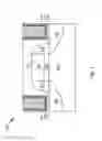
FIG. 3 is a schematic diagram of another exemplary MOSFET 300 with the MIS contact structure for the source/drain 104 according to some embodiments. The MIS contact structure for source/drain 104 in FIG. 3 is similar to the MIS structure in FIG. 1, except that due to a process alignment error a portion of the first metal layer 118 is deposited adjacent to the spacer 110 (e.g., nitride) around the area 302 with a dotted line.
With the adjacent nitride spacer 110 present, the first metal layer 118 at the area 302 does not form a metal oxide layer. However, since the metal oxide layer 116 is formed on the source/drain 104 at the bottom of the first metal layer 118, the MIS contact structure is still functional to lower the Schottky barrier height and associated contact resistance as described above with respect to FIG. 1.
According to some embodiments, a method includes depositing a first metal layer on a native SiO2 layer that is disposed on at least one of a source and a drain of a metal-oxide-semiconductor field-effect transistor (MOSFET). A metal oxide layer is formed from the native SiO2 layer and the first metal layer, wherein the remaining first metal layer, the metal oxide layer, and the at least one of the source and the drain form a metal-insulator-semiconductor (MIS) contact.
According to some embodiments, a metal-oxide-semiconductor field-effect transistor (MOSFET) includes a substrate, a source on the substrate, a drain on the substrate, a raised silicon layer on at least one of the source and the drain, a metal oxide layer on the raised silicon layer, and a first metal layer on the metal oxide layer. The metal layer, the first metal oxide layer, and at least one of the source and the drain form a metal-insulator-semiconductor (MIS) contact.
A skilled person in the art will appreciate that there can be many embodiment variations of this disclosure. Although the embodiments and their features have been described in detail, it should be understood that various changes, substitutions and alterations can be made herein without departing from the spirit and scope of the embodiments. Moreover, the scope of the present application is not intended to be limited to the particular embodiments of the process, machine, manufacture, and composition of matter, means, methods and steps described in the specification. As one of ordinary skill in the art will readily appreciate from the disclosed embodiments, processes, machines, manufacture, compositions of matter, means, methods, or steps, presently existing or later to be developed, that perform substantially the same function or achieve substantially the same result as the corresponding embodiments described herein may be utilized according to the present disclosure.
The above method embodiment shows exemplary steps, but they are not necessarily required to be performed in the order shown. Steps may be added, replaced, changed order, and/or eliminated as appropriate, in accordance with the spirit and scope of embodiment of the disclosure. Embodiments that combine different claims and/or different embodiments are within the scope of the disclosure and will be apparent to those skilled in the art after reviewing this disclosure.
Claims
What is claimed is:1. A semiconductor device comprising:
a source on a substrate;
a drain on the substrate; and
a contact on at least one of the source and the drain, the contact comprising:
a raised silicon layer;
a metal oxide layer extending over the top surface of the raised silicon layer from a first side of the raised silicon layer to a second side of the raised silicon layer; and
a first metal layer on the metal oxide layer.
2. The semiconductor device of claim 1, wherein the first metal layer comprises Ti, Hf, Zr, or Al.
3. The semiconductor device of claim 1, wherein the first metal layer has a thickness ranging from 10 Å to 20 Å.
4. The semiconductor device of claim 1, wherein the raised silicon layer has a thickness ranging from 3 Å to 5 Å.
5. The semiconductor device of claim 1, further comprising a second metal layer on the first metal layer.
6. The semiconductor device of claim 5, wherein the second metal layer comprises Al, Cu, or W.
7. The semiconductor device of claim 1, wherein the metal oxide layer has a thickness ranging from 8 Å to 10 Å.
8. The semiconductor device of claim 1, wherein the metal oxide layer comprises TiO2, HfO2, ZrO2, or Al2O3.
9. A semiconductor device comprising:
a gate structure over a substrate, the gate structure comprising a gate electrode, a gate dielectric, and a gate spacer;
a source/drain region in the substrate;
a raised silicon layer over the substrate and separated from the gate spacer;
a metal oxide layer over the raised silicon layer; and
a first metal layer over the metal oxide layer.
10. The semiconductor device of claim 9, further comprising a second metal layer over the first metal layer.
11. The semiconductor device of claim 9, wherein the first metal layer, the metal oxide layer, and the raised silicon layer form a metal-insulator-semiconductor (MIS) contact.
12. The semiconductor device of claim 9, further comprising a dielectric layer over the source/drain region, the dielectric layer comprising an opening, wherein the raised silicon layer protrudes into the opening.
13. The semiconductor device of claim 12, wherein the first metal layer is on sidewalls of the opening in the dielectric layer.
14. The semiconductor device of claim 13, wherein a first thickness of the first metal layer on sidewalls of the opening is the same as a second thickness of the first metal layer on the bottom of the opening.
15. A semiconductor device comprising:
a gate structure on a substrate;
a source/drain region on the substrate;
a dielectric layer over the substrate;
an opening in the dielectric layer over the source/drain region;
a raised silicon layer disposed within the opening;
a metal oxide layer disposed over the raised silicon layer within the opening; and
a first metal layer disposed over the metal oxide layer within the opening.
16. The semiconductor device of claim 15, wherein the first metal layer is disposed on sidewalls of the at least one opening.
17. The semiconductor device of claim 15, wherein a second metal layer is disposed over the first metal layer.
18. The semiconductor device of claim 15, wherein the first metal layer, the metal oxide layer, and the raised silicon layer form a metal-insulator-semiconductor (MIS) contact.
19. The semiconductor device of claim 15, wherein a first thickness of the first metal layer on sidewalls of the opening is less than a second thickness of the first metal layer on the bottom of the opening.
20. The semiconductor device of claim 15, wherein the gate structure comprises a gate electrode and a gate spacer formed on a sidewall thereof and wherein a portion of the first metal layer contacts the gate spacer.
Images & Drawings included:
Sources:
- United States Patent and Trademark Office - verify current appl. status at the USPTO↗
Recent applications in this class:
- » 20250072093 2025-02-27
DISPLAY PANEL - » 20240429303 2024-12-26
INTEGRATED CIRCUIT DEVICE - » 20240429302 2024-12-26
MEMORY DEVICE AND FORMING METHOD THEREOF - » 20240405090 2024-12-05
SEMICONDUCTOR DEVICE - » 20240395894 2024-11-28
Molybdenum-Containing Device-Level Interconnects and Methods of Fabrication Thereof - » 20240379806 2024-11-14
SEMICONDUCTOR DEVICES HAVING SILICIDE LAYER - » 20240379805 2024-11-14
SILICIDE STRUCTURES IN TRANSISTORS AND METHODS OF FORMING - » 20240371962 2024-11-07
SEMICONDUCTOR DEVICE AND METHOD OF MANUFACTURING THE SAME - » 20240339517 2024-10-10
SEMICONDUCTOR DEVICE AND METHOD FOR MANUFACTURING SEMICONDUCTOR DEVICE - » 20240332393 2024-10-03
Contact Structures In Semiconductor Devices
Recent applications for this Assignee:
- » 20240266341 2024-08-08
HYBRID BONDING WITH UNIFORM PATTERN DENSITY - » 20240224489 2024-07-04
SEMICONDUCTOR DEVICE - » 20240170063 2024-05-23
CONTENT ADDRESSABLE MEMORY ARRAY DEVICE STRUCTURE - » 20240161819 2024-05-16
MEMORY DEVICE AND MANUFACTURING THEREOF - » 20240153896 2024-05-09
SEMICONDUCTOR PACKAGE SYSTEM AND METHOD - » 20240120409 2024-04-11
Method for non-resist nanolithography - » 20240113080 2024-04-04
Semiconductor Device with Discrete Blocks - » 20240105632 2024-03-28
Method for forming a semiconductor device including forming a first interconnect structure on one side of a substrate having first metal feature closer the substrate than second metal feature and forming first and second tsv on other side of substrate connecting to the metal features - » 20240096816 2024-03-21
Method of manufacture overlay mark using laser marking process for semiconductor device - » 20240096383 2024-03-21
MEMORY DEVICE