Electronic device and method of manufacturing the same
US20160141222A1
2016-05-19
15/001,575
2016-01-20
✅ Patent granted
US 9,508,627 B2
2016-11-29
-
-
Nicholas Tobergte
Kratz, Quintos & Hanson, LLP
2036-01-20
Abstract:
In manufacturing an electronic device in which a semiconductor chip including an element layer formed on a front surface of a substrate and a heat sink to perform heat radiation of the semiconductor chip are connected via a heat spreader, a first heat spreader is formed on a rear surface of the semiconductor chip using a first carbon nanotube, a second heat spreader is formed on the heat sink using a second carbon nanotube, and the first heat spreader and the second heat spreader are caused to adhere to each other. With this configuration, a highly reliable electronic device that has very low heat resistance and achieves efficient heat radiation with a relatively simple configuration is fabricated.
Assignee:
- FUJITSU LIMITED 26,672 🇯🇵 Kawasaki, Japan
Applicant:
Interested in similar patents?
Get notified when new applications in this technology area are published.
Classification:
H01L23/3677 » CPC main
Details of semiconductor or other solid state devices; Arrangements for cooling, heating, ventilating or temperature compensation ; Temperature sensing arrangements; Selection of materials, or shaping, to facilitate cooling or heating, e.g. heatsinks; Cooling facilitated by shape of device Wire-like or pin-like cooling fins or heat sinks
H01L21/48 IPC
Processes or apparatus adapted for the manufacture or treatment of semiconductor or solid state devices or of parts thereof; Manufacture or treatment of semiconductor devices or of parts thereof the devices having at least one potential-jump barrier or surface barrier, e.g. PN junction, depletion layer or carrier concentration layer Manufacture or treatment of parts, e.g. containers, prior to assembly of the devices, using processes not provided for in a single one of the subgroups -
H01L23/3737 » CPC further
Details of semiconductor or other solid state devices; Arrangements for cooling, heating, ventilating or temperature compensation ; Temperature sensing arrangements; Selection of materials, or shaping, to facilitate cooling or heating, e.g. heatsinks; Cooling facilitated by selection of materials for the device or materials for thermal expansion adaptation, e.g. carbon Organic materials with or without a thermoconductive filler
H01L21/4882 » CPC further
Processes or apparatus adapted for the manufacture or treatment of semiconductor or solid state devices or of parts thereof; Manufacture or treatment of semiconductor devices or of parts thereof the devices having at least one potential-jump barrier or surface barrier, e.g. PN junction, depletion layer or carrier concentration layer; Manufacture or treatment of parts, e.g. containers, prior to assembly of the devices, using processes not provided for in a single one of the subgroups -; Conductive parts; Bases, plates or heatsinks Assembly of heatsink parts
H01L23/373 » CPC further
Details of semiconductor or other solid state devices; Arrangements for cooling, heating, ventilating or temperature compensation ; Temperature sensing arrangements; Selection of materials, or shaping, to facilitate cooling or heating, e.g. heatsinks Cooling facilitated by selection of materials for the device or materials for thermal expansion adaptation, e.g. carbon
H01L23/367 » CPC further
Details of semiconductor or other solid state devices; Arrangements for cooling, heating, ventilating or temperature compensation ; Temperature sensing arrangements; Selection of materials, or shaping, to facilitate cooling or heating, e.g. heatsinks Cooling facilitated by shape of device
H01L21/4871 » CPC further
Processes or apparatus adapted for the manufacture or treatment of semiconductor or solid state devices or of parts thereof; Manufacture or treatment of semiconductor devices or of parts thereof the devices having at least one potential-jump barrier or surface barrier, e.g. PN junction, depletion layer or carrier concentration layer; Manufacture or treatment of parts, e.g. containers, prior to assembly of the devices, using processes not provided for in a single one of the subgroups -; Conductive parts Bases, plates or heatsinks
H01L23/3736 » CPC further
Details of semiconductor or other solid state devices; Arrangements for cooling, heating, ventilating or temperature compensation ; Temperature sensing arrangements; Selection of materials, or shaping, to facilitate cooling or heating, e.g. heatsinks; Cooling facilitated by selection of materials for the device or materials for thermal expansion adaptation, e.g. carbon Metallic materials
H01L2224/73253 » CPC further
Indexing scheme for arrangements for connecting or disconnecting semiconductor or solid-state bodies and methods related thereto as covered by; Means for bonding being of different types provided for in two or more of groups; Location after the connecting process on different surfaces Bump and layer connectors
H01L2924/0002 » CPC further
Indexing scheme for arrangements or methods for connecting or disconnecting semiconductor or solid-state bodies as covered by; Technical content checked by a classifier Not covered by any one of groups , and
H01L23/48 IPC
Details of semiconductor or other solid state devices Arrangements for conducting electric current to or from the solid state body in operation, e.g. leads, terminal arrangements ; Selection of materials therefor
H01L23/42 » CPC further
Details of semiconductor or other solid state devices; Arrangements for cooling, heating, ventilating or temperature compensation ; Temperature sensing arrangements Fillings or auxiliary members in containers or encapsulations selected or arranged to facilitate heating or cooling
Description
CROSS-REFERENCE TO RELATED APPLICATIONS
This application is a continuation application of International Application PCT/JP2013/083585 filed on Dec. 16, 2013 and designated the U.S., which claims the benefit of priority of the prior Japanese Patent Application No. 2013-152986, filed on Jul. 23, 2013, the entire contents of which are incorporated herein by reference.
FIELD
The embodiment discussed herein is directed to an electronic device and a method of manufacturing the same.
BACKGROUND
In recent years, there are electronic devices, for example, a semiconductor device and the like in which a heat spreader with TIM1 and TIM2 being a highly heat conductive adhesive material added to its upper and lower surfaces is provided between a semiconductor element and a heat sink as a heat radiation technique. Further, there is also devised a heat radiation technique in which a carbon nanotube (CNT) is formed between a semiconductor element and a heat sink (see, for example, Patent Documents 1 to 3).
[Patent Document 1] Japanese Laid-open Patent Publication No. 2010-192656
[Patent Document 2] Japanese Laid-open Patent Publication No. 2010-192661
[Patent Document 3] Japanese Laid-open Patent Publication No. 2010-267706
However, the above-described heat radiation techniques using the CNT each have a problem that heat resistance increases at a joint place between the semiconductor element and the heat sink, to thereby make it impossible to perform sufficient heat radiation.
SUMMARY
An electronic device, comprising:
an electronic part including an element layer formed on a front surface of a substrate;
a heat sink performing heat radiation of the electronic part; and
a heat spreader provided between a rear surface of the electronic part and the heat sink;
wherein the heat spreader comprises a first heat spreader formed on the rear surface of the electronic part and the first heat spreader comprising a first carbon nanotube; and
a second heat spreader formed on the heat sink and the second heat spreader comprising a second carbon nanotube.
A method of manufacturing an electronic device of the embodiment is a method of manufacturing an electronic device in which an electronic part including an element layer formed on a front surface of a substrate and a heat sink to perform heat radiation of the electronic part are connected via a heat spreader, the method including:
forming a first heat spreader on a rear surface of the electronic part using a first carbon nanotube;
forming a second heat spreader on the heat sink using a second carbon nanotube; and
causing the first heat spreader and the second heat spreader to adhere to each other.
The object and advantages of the invention will be realized and attained by means of the elements and combinations particularly pointed out in the claims.
It is to be understood that both the foregoing general description and the following detailed description are exemplary and explanatory and are not restrictive of the invention.
BRIEF DESCRIPTION OF DRAWINGS
FIG. 1A is a schematic cross-sectional view illustrating a method of manufacturing an electronic device according to an embodiment in order of processes;
FIG. 1B is a schematic cross-sectional view illustrating, subsequent to FIG. 1A, the method of manufacturing the electronic device according to the embodiment in order of processes;
FIG. 1C is a schematic cross-sectional view illustrating, subsequent to FIG. 1B, the method of manufacturing the electronic device according to the embodiment in order of processes;
FIG. 2A is a schematic cross-sectional view illustrating, subsequent to FIG. 1C, the method of manufacturing the electronic device according to the embodiment in order of processes;
FIG. 2B is a schematic cross-sectional view illustrating, subsequent to FIG. 2A, the method of manufacturing the electronic device according to the embodiment in order of processes;
FIG. 2C is a schematic cross-sectional view illustrating, subsequent to FIG. 2B, the method of manufacturing the electronic device according to the embodiment in order of processes;
FIG. 3A is a schematic cross-sectional view illustrating, subsequent to FIG. 2C, the method of manufacturing the electronic device according to the embodiment in order of processes;
FIG. 3B is a schematic cross-sectional view illustrating, subsequent to FIG. 3A, the method of manufacturing the electronic device according to the embodiment in order of processes;
FIG. 4A is a schematic cross-sectional view illustrating, subsequent to FIG. 3B, the method of manufacturing the electronic device according to the embodiment in order of processes;
FIG. 4B is a schematic cross-sectional view illustrating, subsequent to FIG. 4A, the method of manufacturing the electronic device according to the embodiment in order of processes;
FIG. 4C is a schematic cross-sectional view illustrating, subsequent to FIG. 4B, the method of manufacturing the electronic device according to the embodiment in order of processes;
FIG. 4D is a schematic cross-sectional view illustrating, subsequent to FIG. 4C, the method of manufacturing the electronic device according to the embodiment in order of processes;
FIG. 5A is a schematic cross-sectional view illustrating, subsequent to FIG. 4D, the method of manufacturing the electronic device according to the embodiment in order of processes; and
FIG. 5B is a schematic cross-sectional view illustrating, subsequent to FIG. 5A, the method of manufacturing the electronic device according to the embodiment in order of processes.
DESCRIPTION OF EMBODIMENT
Hereinafter, a concrete embodiment to which the embodiment is applied will be explained in detail with reference to the drawings.
In this embodiment, as an electronic device, a semiconductor device provided with a transistor element having a MOS structure as a functional element will be disclosed together with its manufacturing method. Incidentally, as the semiconductor device, ones having various memory elements, capacitor elements, and the like as a functional element can be applied other than the MOS transistor in this embodiment.
FIG. 1A to FIG. 5B are schematic cross-sectional views illustrating the method of manufacturing the semiconductor device according to this embodiment in order of processes.
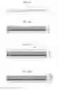
First, each semiconductor chip is formed.
As illustrated in FIG. 1A, a semiconductor substrate including an element layer 11 formed on a front surface thereof, which is, for example, a silicon substrate 1, is prepared.
The element layer 11 is one made in a manner that the transistor element having a MOS structure as a functional element, its wiring structure, and the like are formed in an insulating film, for example.
Subsequently, as illustrated in FIG. 1B, the front surface side of the silicon substrate 1 (the element layer 11 side) is mounted and fixed to a supporting substrate 30.
Subsequently, as illustrated in FIG. 1C, a rear surface of the silicon substrate 1 is ground by back-grinding, and thereby the silicon substrate 1 is thinned to a predetermined thickness.
Subsequently, as illustrated in FIG. 2A, a CNT 14 is made to grow at the rear surface of the silicon substrate 1.
In more detail, first, for example, Ti, TiN, Ta, TaN, or the like is deposited into a thickness of several nanometers or so to 20 nm or so by a sputtering method or the like. Thereby, a base material 12 being a barrier metal is formed on the rear surface of the silicon substrate 1.
Next, a catalyst material is deposited into a thickness of several nanometers or so, for example, by a vacuum deposition method or the like. As the catalyst material, a mixed material of one kind or two or more kinds selected from among Co, Ni, Fe, Ti, V, and so on is used. For example, Co/Ti or Co/V is selected. Thereby, a catalyst material 13 is formed on the base material 12 at the rear surface of the silicon substrate 1.
Next, for example, by a thermal CVD method, growth processing of the carbon nanotube (CNT) is performed with a growth temperature set to a value in a low-temperature range of 400° C. to 450° C., which is 450° C. or so here. Thereby, the CNT 14 is formed so as to stand up from the catalyst material 13 existing at the rear surface of the silicon substrate 1. The CNT 14 is formed to a length of several micrometers or so to several hundred micrometers or so, for example. The CNT is a material higher in heat conductivity and better in heat radiation performance than silicon that is the substrate material.
Subsequently, as illustrated in FIG. 2B, a metal material 15 used for the CNT 14 to be embedded therein is formed.
In more detail, as the metal material 15 high in heat conductivity, for example, Cu is formed at the rear surface of the silicon substrate 1 so that the CNT 14 is embedded therein by an electrolytic plating method or the like. Thereby, a composite material of the CNT 14 and the metal material 15 with the CNT 14 embedded therein is formed at the rear surface of the silicon substrate 1. As the metal material 15, for example, Ag, Au, or the like can be used in place of Cu. Further, in place of plating, a metal nanoparticle dispersion liquid or the like can also be used.
Subsequently, as illustrated in FIG. 2C, the extra metal material 15 of the composite material is removed.
In more detail, by a chemical mechanical polishing (CMP) method, for example, the metal material 15 of the composite material is polished and removed until a tip of the CNT 14 in the composite material is exposed. Thereby, a first heat spreader 2 that is made of the composite material and has a flat front surface from which the tip of the CNT 14 is exposed is formed.
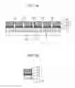
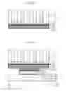
Subsequently, as illustrated in FIG. 3A, the silicon substrate 1 is subjected to a dicing process to be diced into individual semiconductor chips along each dicing line 1a.
Subsequently, as illustrated in FIG. 3B, each semiconductor chip 10 is separated from the supporting substrate 30.
The semiconductor chip 10 is made by the element layer 11 being formed on the front surface of the silicon substrate 1. The first heat spreader 2 is formed on a rear surface of the semiconductor chip 10.
Next, a heat sink is formed.
As illustrated in FIG. 4A, a base 3 for the heat sink is prepared. The base 3 is made of a metal material high in heat conductivity such as Cu or Al, for example.
Subsequently, as illustrated in FIG. 4B, a CNT 23 is made to grow at a rear surface of the base 3.
In more detail, first, for example, Ti, TiN, Ta, TaN, or the like is deposited into a thickness of several nanometers or so to 20 nm or so by a sputtering method or the like. Thereby, a base material 21 being a barrier metal is formed on the rear surface of the base 3.
Next, a catalyst material is deposited into a thickness of several nanometers or so, for example, by a vacuum deposition method or the like. As the catalyst material, a mixed material of one kind or two or more kinds selected from among Co, Ni, Fe, Ti, V, and so on is used. For example, Co/Ti or Co/V is selected. Thereby, a catalyst material 22 is formed on the base material 21 at the rear surface of the base 3.
Next, for example, by a thermal CVD method, growth processing of the carbon nanotube (CNT) is performed with a growth temperature set to a value in a low-temperature range of 400° C. to 450° C., which is 450° C. or so here. Thereby, the CNT 23 is formed so as to stand up from the catalyst material 22 existing at the rear surface of the base 3. The CNT 23 is formed to a length of several micrometers or so to several hundred micrometers or so, for example. The CNT is a material higher in heat conductivity and better in heat radiation performance than Cu or the like that is the base material.
Subsequently, as illustrated in FIG. 4C, a metal material 24 used for the CNT 23 to be embedded therein is formed.
In more detail, as the metal material 24 high in heat conductivity, for example, Cu is formed at the rear surface of the base 3 so that the CNT 23 is embedded therein by an electrolytic plating method or the like. Thereby, a composite material of the CNT 23 and the metal material 24 with the CNT 23 embedded therein is formed at the rear surface of the base 3. As the metal material 24, for example, Ag, Au, or the like can be used in place of Cu. Further, in place of plating, a metal nanoparticle dispersion liquid or the like can also be used.
Subsequently, as illustrated in FIG. 4D, the extra metal material 24 of the composite material is removed.
In more detail, by a CMP method, for example, the metal material 24 of the composite material is polished and removed until a tip of the CNT 23 in the composite material is exposed. Thereby, a second heat spreader 4 that is made of the composite material and has a flat front surface from which the tip of the CNT 23 is exposed is formed.
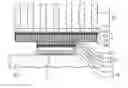
Subsequently, as illustrated in FIG. 5A, a heat radiation fin 5 is formed on a front surface of the base 3. The heat radiation fin 5 is desirably formed of the same metal high in heat conductivity as that of the base 3. In this manner, a heat sink 20 made by the heat radiation fin 5 being provided on the front surface of the base 3 is formed. On a rear surface of the heat sink 20, the second heat spreader 4 is formed.
Subsequently, as illustrated in FIG. 5B, the front surface of the first heat spreader 2 on the semiconductor chip 10 and the front surface of the second heat spreader 4 on the heat sink 20 are faced each other and the both are brought into contact with each other directly. The front surfaces of the first and second heat spreaders 2, 4 are each made flat by the CMP method to be brought into a state excellent in flatness, and the both are brought into contact with each other at a predetermined pressure in a vacuum atmosphere, to thereby adhere and be fixed. At this time, it is also possible that an indium layer is formed at a joint surface and thermal joining is performed simultaneously with pressurization.
On terminals on the front surface of the element layer 11 of the semiconductor chip 10, for example, solder balls 6 are provided to be electrically connected to a predetermined mounting substrate 40. In this manner, the semiconductor device in this embodiment is formed.
In the semiconductor device in this embodiment, the front surfaces of the first and second heat spreaders 2, 4 are faced each other to adhere and be fixed, and thereby a heat spreader is constituted. In this case, there is no inclusion with high heat resistance in the heat spreader itself constituted by the first and second heat spreaders 2, 4, between the heat spreader and the semiconductor chip 10, and between the heat spreader and the heat sink 20. According to this embodiment as above, it is possible to obtain a highly reliable semiconductor device that has very low heat resistance and achieves efficient heat radiation with a relatively simple configuration.
According to the embodiment, there is fabricated a highly reliable electronic device that has very low heat resistance and enables efficient heat radiation with a relatively simple configuration.
All examples and conditional language provided herein are intended for the pedagogical purposes of aiding the reader in understanding the invention and the concepts contributed by the inventor to further the art, and are not to be construed as limitations to such specifically recited examples and conditions, nor does the organization of such examples in the specification relate to a showing of the superiority and inferiority of the invention. Although one or more embodiments of the present invention have been described in detail, it should be understood that the various changes, substitutions, and alterations could be made hereto without departing from the spirit and scope of the invention.
Claims
What is claimed is:1. An electronic device, comprising:
an electronic part including an element layer formed on a front surface of a substrate;
a heat sink performing heat radiation of the electronic part; and
a heat spreader provided between a rear surface of the electronic part and the heat sink,
wherein the heat spreader comprises
a first heat spreader formed on the rear surface of the electronic part and comprising a first carbon nanotube, and
a second heat spreader formed on the heat sink and comprising a second carbon nanotube.
2. The electronic device according to claim 1, wherein
the first heat spreader comprises a first composite material of the first carbon nanotube and a first metal,
the second heat spreader comprises a second composite material of the second carbon nanotube and a second metal, and
the first composite material and the second composite material both have a flat surface and the flat surface of the first composite material and the flat surface of the second composite material are caused to adhere to each other.
3. The electronic device according to claim 2, wherein
the flat surface of the first composite material and the flat surface of the second composite material are caused to directly adhere to each other.
4. A method of manufacturing an electronic device being a method of manufacturing an electronic device in which an electronic part including an element layer formed on a front surface of a substrate and a heat sink to perform heat radiation of the electronic part are connected via a heat spreader, the method comprising:
forming a first heat spreader on a rear surface of the electronic part using a first carbon nanotube;
forming a second heat spreader on the heat sink using a second carbon nanotube; and
causing the first heat spreader and the second heat spreader to adhere to each other.
5. The method of manufacturing the electronic device according to claim 4, wherein
the first heat spreader is formed using a first composite material of the first carbon nanotube and a first metal,
the second heat spreader is formed using a second composite material of the second carbon nanotube and a second metal, and
the first composite material and the second composite material both have a flat surface and the flat surface of the first composite material and the flat surface of the second composite material are caused to adhere to each other.
6. The method of manufacturing the electronic device according to claim 5, wherein
the flat surface of the first composite material and the flat surface of the second composite material are caused to directly adhere to each other.
Images & Drawings included:
Sources:
- United States Patent and Trademark Office - verify current appl. status at the USPTO↗
Similar patent applications:
- » 20160291461
PATTERN FORMING METHOD, ELECTRONIC DEVICE MANUFACTURING METHOD, ELECTRONIC DEVICE, BLOCK COPOLYMER AND BLOCK COPOLYMER PRODUCTION METHOD - » 20150093692
PATTERN FORMING METHOD, ACTINIC RAY-SENSITIVE OR RADIATION-SENSITIVE RESIN COMPOSITION AND RESIST FILM USED THEREFOR, AND ELECTRONIC DEVICE MANUFACTURING METHOD AND ELECTRONIC DEVICE USING THE SAMEDEVICE MANUFACTURING METHOD AND ELECTRONIC DEVICE USING THE SAME - » 20110163456
Electronic device substrate, electronic device, method of manufacturing electronic device substrate, method of manufacturing electronic device, and electronic apparatus - » 20130136900
ACTINIC RAY-SENSITIVE OR RADIATION-SENSITIVE RESIN COMPOSITION, AND RESIST FILM, PATTERN FORMING METHOD, ELECTRONIC DEVICE MANUFACTURING METHOD, AND ELECTRONIC DEVICE, EACH USING THE COMPOSITION - » 20130078433
Actinic-ray-sensitive or radiation-sensitive resin composition, and resist film using the same, pattern forming method, electronic device manufacturing method, and electronic device, each using the same - » 20110033656
PATTERN FORMING METHOD, ELECTRONIC DEVICE MANUFACTURING METHOD AND ELECTRONIC DEVICE - » 20130078434
Actinic ray-sensitive or radiation-sensitive resin composition, and, resist film, pattern forming method, electronic device manufacturing method, and electronic device, each using the same - » 20120228782
METHOD FOR MANUFACTURING ELECTRONIC DEVICE, ELECTRONIC DEVICE, METHOD FOR MANUFACTURING ELECTRONIC DEVICE PACKAGE AND ELECTRONIC DEVICE PACKAGE - » 20080182082
Pattern forming method, electronic device manufacturing method and electronic device - » 20140287363
Actinic ray-sensitive or radiation-sensitive resin composition, and, resist film, pattern forming method, electronic device manufacturing method, and electronic device, each using the composition
Recent applications in this class:
- » 20250285932 2025-09-11
SEMICONDUCTOR DEVICE AND ELECTRIC POWER CONVERSION UNIT - » 20250285931 2025-09-11
ELECTRONIC PACKAGE WITH INTEGRATED TOP SIDE HEAT SINK - » 20250279330 2025-09-04
ENHANCED INTEGRATED CIRCUIT HEAT DISSIPATION USING INACTIVE METAL LINES - » 20250233041 2025-07-17
COOLING DEVICE - » 20250233040 2025-07-17
SEMICONDUCTOR PACKAGE STRUCTURE - » 20250226281 2025-07-10
SEMICONDUCTOR DEVICE - » 20250191995 2025-06-12
THERMAL TRANSFER VIAS AND SEMICONDUCTOR VIA STRUCTURE FOR ENHANCED THERMAL TRANSFER - » 20250191994 2025-06-12
SEMICONDUCTOR STRUCTURE AND METHOD OF FORMING THE SAME - » 20250140638 2025-05-01
SEMICONDUCTOR DEVICE - » 20250140637 2025-05-01
COOLING MODULE FOR HETEROGENEOUS INTEGRATED SEMICONDUCTOR PACKAGE STRUCTURE
Recent applications for this Assignee:
- » 20250284769 2025-09-11
ARITHMETIC PROCESSING DEVICE AND ARITHMETIC PROCESSING METHOD - » 20250278454 2025-09-04
COMPUTING SYSTEM AND METHOD FOR CONTROLLING COMPUTING SYSTEM - » 20250238593 2025-07-24
COMPUTER-READABLE RECORDING MEDIUM STORING INFORMATION PROCESSING PROGRAM AND INFORMATION PROCESSING METHOD - » 20250141547 2025-05-01
OPTICAL TRANSMISSION LINE MONITORING DEVICE AND OPTICAL TRANSMISSION LINE MONITORING METHOD - » 20250141543 2025-05-01
OPTICAL TRANSMISSION LINE MONITORING DEVICE AND OPTICAL TRANSMISSION LINE MONITORING METHOD - » 20250139433 2025-05-01
MODEL GENERATION METHOD AND INFORMATION PROCESSING APPARATUS - » 20250131194 2025-04-24
COMPUTER-READABLE RECORDING MEDIUM STORING INFORMATION PROCESSING PROGRAM, INFORMATION PROCESSING METHOD, AND INFORMATION PROCESSING DEVICE - » 20250130843 2025-04-24
COMPUTER-READABLE RECORDING MEDIUM STORING INFORMATION PROCESSING PROGRAM, INFORMATION PROCESSING METHOD, AND MANAGEMENT DEVICE - » 20250124710 2025-04-17
NON-TRANSITORY COMPUTER-READABLE RECORDING MEDIUM STORING GENERATION PROGRAM, GENERATION METHOD, AND INFORMATION PROCESSING DEVICE - » 20250037000 2025-01-30
COMPUTER-READABLE RECORDING MEDIUM STORING PARTITIONING PROGRAM FOR MULTI-QUBIT OBSERVABLES, PARTITIONING METHOD FOR MULTI-QUBIT OBSERVABLES, AND INFORMATION PROCESSING DEVICE